Qualitative models and experimental investigation of chaotic NOR gates and set/reset flip-flops
Abstract
It has been observed through experiments and SPICE simulations that logical circuits based upon Chua’s circuit exhibit complex dynamical behavior. This behavior can be used to design analogs of more complex logic families and some properties can be exploited for electronics applications. Some of these circuits have been modeled as systems of ordinary differential equations. However, as the number of components in newer circuits increases so does the complexity. This renders continuous dynamical systems models impractical and necessitates new modeling techniques. In recent years some discrete dynamical models have been developed using various simplifying assumptions. To create a robust modeling framework for chaotic logical circuits, we developed both deterministic and stochastic discrete dynamical models, which exploit the natural recurrence behavior, for two chaotic NOR gates and a chaotic set/reset flip-flop (RSFF). This work presents a complete applied mathematical investigation of logical circuits. Experiments on our own designs of the above circuits are modeled and the models are rigorously analyzed and simulated showing surprisingly close qualitative agreement with the experiments. Furthermore, the models are designed to accommodate dynamics of similarly designed circuits. This will allow researchers to develop ever more complex chaotic logical circuits with a simple modeling framework.
Keywords: Set/Reset flip-flop circuit, NOR gate, chaos, stochastic dynamical system
Pacs numbers: 05.45.Ac, 05.45.Pq, 84.30.-r
1 Introduction
Since the 1990s there has been growing interest in controlling chaotic circuits starting from synchronization [1, 2], and leading to logical circuits [3]. Constructions of chaotic logical circuits mainly employ the usual circuit elements such as resistors, capacitors, and inductors, and a less common component called a nonlinear resistor. The most well-known nonlinear resistor is Chua’s diode, invented by Leon Chua in 1983 and used as an integral element in Chua’s circuit [4, 5, 6, 7]. For more complex logical circuits, components called threshold control units (TCUs)[8] have been employed [9, 10, 11].
This may seem counterintuitive since throughout the latter half of the 20th century we have constructed ever more stable electronic components to be used in computers and other devices. This has been a triumph for electrical engineering and physics. However, not all logical systems are electronic nor man-made [12], and as we may observe, nature is often unstable. Since it is easier to study electrical systems, these chaotic logical circuits can help us better understand naturally occurring logical systems. Furthermore, the chaotic/logical properties of the circuits can be exploited for the purposes of encryption or secure communication.
While there has been an abundance of SPICE simulations and some experimental investigations in the literature, such as [3, 9, 10], there is a dearth of models for the more complex chaotic logical circuits. This is understandable since the usual modeling techniques become ever more difficult to implement as the number of components increase. Traditionally, logical circuits have been modeled as systems of ordinary differential equations (see [13, 3]) because resistors, capacitors, and inductors are related via different rates of change. Furthermore, SPICE simulations are often employed as a means of studying circuit designs, but the computational costs become unreasonable as circuits become more complex. However, more recently, there has been some effort in modeling logical circuits as simple discrete dynamical systems [14, 15, 16] and developing a mathematical framework for studying chaos in boolean networks [17, 18].
To facilitate the development of models of more complex chaotic logical circuits, we created a modeling framework by investigating two chaotic NOR gates and a chaotic Set/Reset flip-flop (RSFF). We modified the chaotic RSFF/dual NOR gate design of Cafagna and Grassi [11] and simulated our design in MultiSIM (a software based on SPICE) to verify agreement with the PSPICE simulations of [11]. Once the design was satisfactory, we built the circuits and recorded the same measurements as the simulations for the sake of having compatible data sets. These empirical observations and information about the physics from previous investigations were then used to develop the models. This was followed by analysis and simulations of our models, which showed surprising agreement with the experiments and SPICE based simulations.
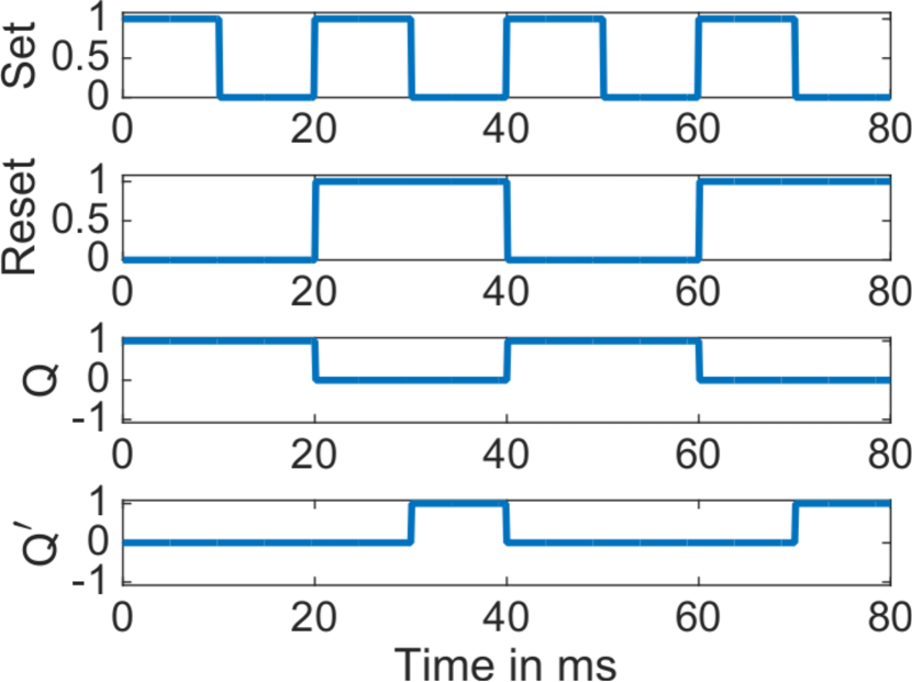
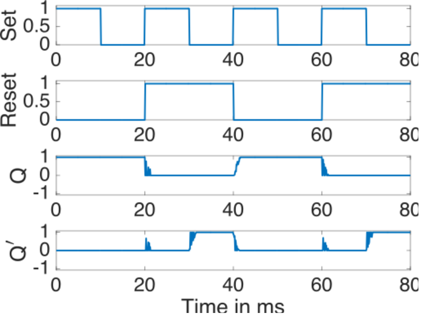
Since the full schematic of the circuits (3 in 1) is quite complex and similar to those in the aforementioned works, it have been relegated to the appendix. However, the “black box” schematics of both types of circuits are quite simple, and will be referred to throughout this work. For example, a NOR gate acts as the negation of the disjunctive operator, i.e. it will output high voltage if and only if it receives low voltage inputs. The RSFF employs two NOR gates with feedbacks as shown in Fig 1.
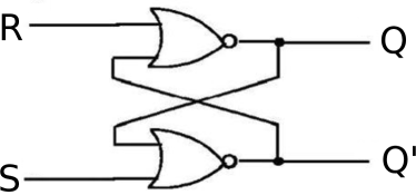
| R | S | Q | Q’ |
|---|---|---|---|
| 0 | 0 | Keep previous state | |
| 0 | 1 | 1 | 0 |
| 1 | 0 | 0 | 1 |
| 1 | 1 | Not allowed | |
The body of this work is organized into two main parts: experiments and extensive modeling, analysis, and simulations. In section 2 we briefly refer to past SPICE simulations and discuss experimental results of our circuit designs in order to motivate the models. Section 3 contains the focus of this article. We first derive deterministic discrete dynamical models for two types of chaotic NOR gates and analyze certain properties of the models including the existence of chaotic dynamics. Then we use the NOR gate models to derive the RSFF model and compare their simulations with the experiments. Next, in Section 4 we derive a stochastic discrete dynamical model for the RSFF in order to incorporate races (when two parallel signals do not have the same “speed”) and compare their simulations with experiments. We end by discussing unexpected predictive capabilities of the models for components that were not explicitly accounted for.
2 Experiments and SPICE Simulations
In this section we discuss previous PSPICE simulations for chaotic NOR gate and RSFF constructions and present our own design and experimental results to demonstrate the robustness of the circuit design even in the midst of chaos.
2.1 Previous investigations
Murali et al. developed and tested a chaotic NOR gate construction in [9] and with more detail in [10]. Then Cafagna and Grassi designed an RSFF [11] using similar principles to the NOR gate of Murali et al. , which is now the inspiration for our own RSFF.
The RSFF is designed with Chua’s circuit at its core and two TCUs to realize each NOR gate. Two switches are used to convert the circuit from operating as two separate NOR gates to operating as an RSFF and vice versa. Cafagna and Grassi provide plots of the inputs, outputs, and threshold voltages for both NOR gates, the inputs and outputs of the RSFF, and finally the voltages across the two capacitors. We recreate the same types of plots for our design in order to facilitate comparisons.
2.2 Set/reset flip-flop design and experiment
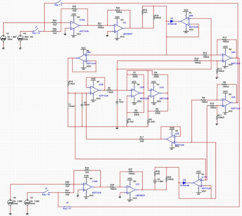
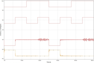
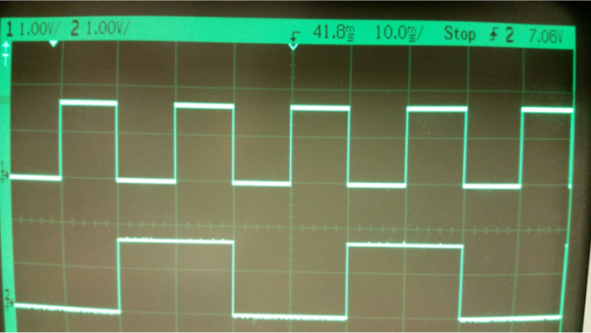
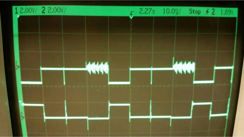
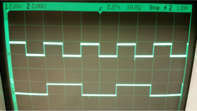
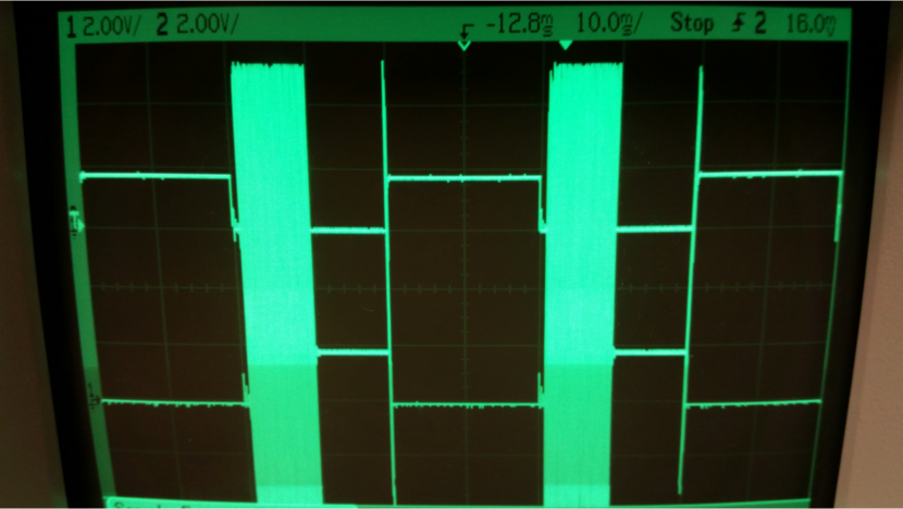
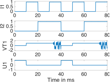
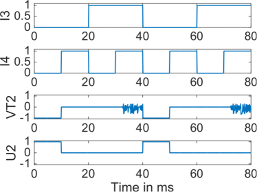
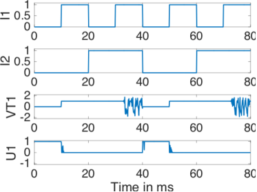
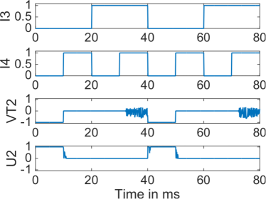
Since the circuit of Cafagna and Grassi [11] uses components that have become unavailable, we needed to design a modern chaotic RSFF/dual NOR gate. The schematic of our circuit design is shown in Fig. 11. For the MultiSIM simulations we use the components shown in Table 2. The chaotic backbone of the circuit comes from Chua’s circuit, and we employ threshold control units to produce the logical outputs. The MultiSIM plots for the dual NOR gate are shown in Fig. 12. We then made a physical realization of the circuit with mostly the same components (Table 2) as the MultiSIM simulations. The experimental setup is shown in Fig. 13. In order to power the circuit and get readings we used a DC power supply, wave form generator, Arduino Due®, and an oscilloscope. From the physical realization we reproduced the MultiSIM plots. To activate the dual NOR gate we keep switches 1 and 2 in Fig. 11 closed and switches 3 and 4 open. The experimental results for the dual NOR gate setup are shown in Fig. 2. In Figs. 2(c) and 2(d) we notice windows of what looks like chaotic dynamics. This is also observed in the MultiSIM simulations. It should be noted that the threshold behavior of the MultiSIM circuit and the physical realization are slightly different due to a change in op-amps. We take a detailed look at the dynamics in Sec. 3.
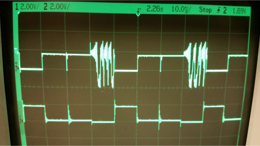
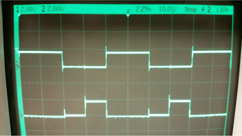
To deactivate the dual NOR gate we open switches 1 and 2 in Fig. 11. To properly activate the RSFF we need to close switches 3 and 4, however we get the RSFF outputs even with the switches open. When we close the switches we notice the race conditions for the “1-1” input causing wild oscillations, which is completely missed in the simulations. This shows that the design has implicit feedbacks, through the op-amps, which results in RSFF operations. However, when the two NOR gates are explicitly connected with one another (i.e. the output of one NOR gate feeds back to the input of the other NOR gate) the race condition exacerbates the oscillations. The experimental results for the RSFF setup are shown in Fig. 3. While the experiments of the RSFF mainly work as expected, the MultiSIM simulations are not able to properly capture this behavior.
3 Deterministic models
We first model the NOR gates, then we use those models to model the RSFF. This is accomplished by constructing continuous extensions and approximating the behavior of the TCU and Chua’s circuit. We have also provided simplified schematics in Fig. 4 to help illustrate the modeling process. It should be noted, that while in the experiments we use a high voltage of volts, in our models this is normalized to .
One may suggest solving Matsumoto’s equation [4] for Chua’s circuit as part of the model. While this would be a legitimate approach, the goal of the article is to formulate the simplest model in terms of derivation and simulation. Having to solve the ordinary differential equation at each time step would be reasonable for a two gate circuit, but would not be scalable to large chaotic logical circuits with many gates. For these reasons, we forgo explicitly modeling the capacitor voltages, and instead develop models for the threshold voltages and the outputs, then show that the derived capacitor voltages agree reasonably well with experiments and MultiSIM simulations in addition to showing the threshold and outputs agree surprisingly well with the experiments and simulations.


3.1 NOR gate
Here we derive and analyze the NOR gate models. The schematic for the gates given in Fig. 11 may be simplified to Fig. 4(a) in order to get a general picture of the circuit. It should be noted that the blocks are not absolutely accurate as the block labeled “Chua” has additional op-amps to that of the traditional Chua circuit and feedback from the “Chua” block to the threshold blocks are not explicitly shown.
3.1.1 Derivation
We begin by formulating the simplest continuous extension of the NOR operator: . This gives us the equation,
| (1) |
where are the respective outputs and are the respective inputs as shown in Fig. 4(a). This naïve extension is enough to approximate the behavior for the NOR gate outputs, and we shall also modify them later to simulate certain subtle aspects of the circuit. However, the more interesting dynamics are observed in the TCUs.
First, let us define the maps, and , where the chosen intervals are the operating domains of the TCUs by design. We apply these maps to the inputs and current time threshold voltages to get the next time threshold voltages,
| (2) |
where and are the respective threshold voltages as shown in Fig. 4(a).
Next, we tabulate our observations from Figs. 2 and 12 in (3), and formulate functions and that qualitatively reproduce the observed behavior. It should be noted that henceforth we shall denote a seemingly random voltage (in the chaotic regime) by a star (), where is not a number to be measured, but rather denotes chaotic behavior.
| (3) |
In order to satisfy these criteria, we first define the maps, and , then
| (4) |
satisfies each property except chaotic behavior.
Now, we must formulate and such that (4) reproduces the qualitative behavior of the threshold voltages for and as shown in Fig. 2. We postulate and will be tent map - like, which is reasonable in the physical sense since these op-amps influence the signal in an approximately piecewise linear manner. Furthermore, the NOR gate developed by Murali et al. employed a TCU designed to behave in a similar manner to that of a logistic map [9], and a tent map is topologically conjugate to a logistic map. For we write,
| (5) |
and we write as,
| (6) |
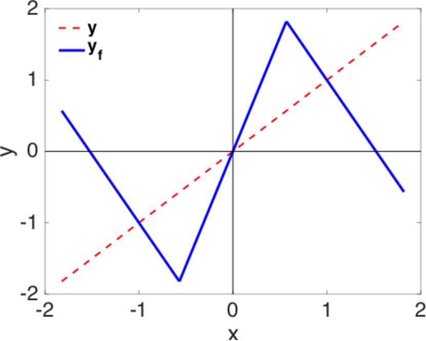
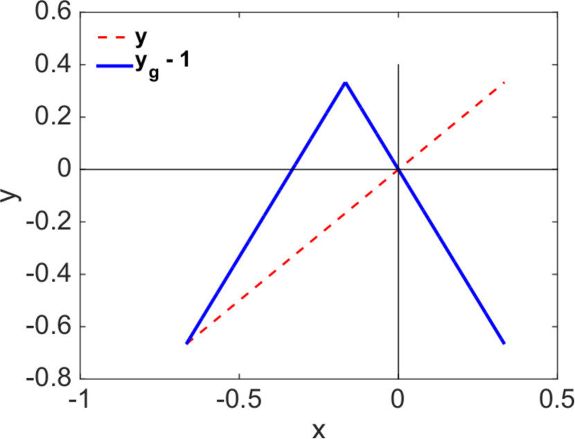
We illustrate (5) and (6) in Fig. 5. In Fig. 5(a) and (5), is the slope of the middle line segment and it also determines the slope of the other two line segments, whereas mainly affects the domain of the map. In Fig. 5(b) and (6), is twice the height of the map and is the amount the new interval is translated from the interval . Moreover, all parameters are positive.
This gives us a model of the thresholding in the two NOR gate operation of the circuit.
3.1.2 Basic properties
Since the interesting behavior arises for and , it suffices to analyze and . First we search for the fixed points. From empirical observations we require and to have a fixed point at the origin and to have two other nonzero fixed points. By definition, the latter has a fixed point at the origin and two nonzero fixed points. However, for the former, we require the right branch to intersect the origin. In order to achieve this, we set for (the right branch),
Furthermore, in order to ensure the inequality, , we require , i.e. .
Now let us identify any additional fixed points for , which necessarily lies on the left branch, i.e. ,
Next, we identify the two nonzero fixed points for . For ,
For the sake of convenience, we outline the fixed points in Table 1.
To analyze the stability of the fixed points of , let us take the derivative,
| (7) |
Both fixed points are sources when . For , there is a line of fixed points on the left branch such that it constitutes a global attracting set. Clearly, this case is unphysical, and hence we require .
Taking the derivative for gives,
| (8) |
By definition, , since otherwise the two outer branches would be undefined. If , there is a line of fixed points on the middle branch, and hence this too is unphysical. Therefore, we require , which shows the origin is a source. For the other two fixed points, if they are be sinks and if they are sources. Notice that only when , which we showed was impossible. Now, if , , which is false. If , , which is true. Therefore, these fixed points are always sources.
The fixed points along with the conditions on the parameters required to yield physical results are summarized in the table below,
| Equation | Fixed points | Conditions |
|---|---|---|
| and |
3.1.3 Chaos
Here we shall prove the maps and become chaotic for certain parameters. First we prove this for , which employs a simple translation to the tent map.
Theorem 1.
The map is chaotic for . In addition, it has a nonwandering set in the form of a translated Cantor set on for . Moreover, for , the nonwandering set is the middle-third Cantor set translated to the interval .
Proof.
Consider the translation , defined as , applied to . This produces the map , which is exactly the tent map. Since is a homeomorphism, it suffices to analyze the tent map. It is well known that when , the tent map is chaotic. Furthermore, for , the nonwandering set is a Cantor set, and for , it is precisely the middle-third Cantor set. This shows the map is also chaotic for , and has a nonwandering set in the form of a translated Cantor set, thereby completing the proof. ∎
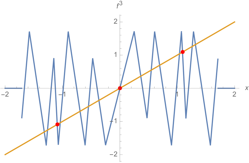
Now we prove is chaotic in the physical parameter regime outlined in Table 1. For the sake of brevity, we assume the parameters are in this regime for our next theorem. The main idea of the proof is to search for 3-cycles and use the main theorem by Li and Yorke [19]. Since the formula for becomes overly complex, we shall use properties of to show the existence of a 3-cycle rather than finding it explicitly, and we provide visual aids to illustrate the proof.
Theorem 2.
For every there exists a periodic point of the map having period and contains chaotic orbits of . Furthermore, there exists an uncountable set containing no periodic orbits.
Proof.
It is shown in [19] that a 3-cycle implies chaos. Now, we show there exists a 3-cycle for all parameter values in the physical regime. This is done by finding the roots of not including the fixed points, or rather showing they exist.
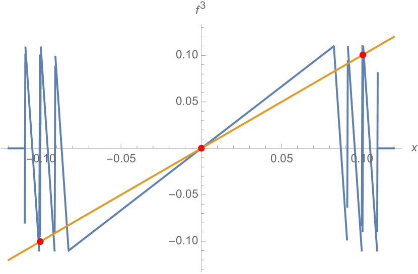
First, let be the set of roots of , then is the set of points having period . We observe (Fig. 6) has linear branches. Since these are linear, each branch may intersect the line at most once. The two outermost branches will never intersect the line for the parameter regime outlined in Table 1. Then and (i.e. has three fixed points), hence . Notice, a 3-cycle exists only if due to the symmetry.
We observe (Fig. 6(a)) for the parameters near that used in simulations. If and are varied forward we maintain . If we vary them backward, the first instance occurs when the cusps of the second and third branches from the left, and respectively from the right, lie on the line . The cusps are located at
Then, solving for , gives , which is unphysical. Since in the parameter regime of Table 1, 3-cycles (in fact, four of them) exist. Therefore, the hypotheses of [19] is satisfied, thereby completing the proof. ∎
3.2 Set/reset flip-flop
Now that we have a model for the NOR gates we can derive the model of the RSFF. Just as with the NOR gate, we sketch a simplified schematic of the RSFF in Fig. 4(b). For the traditional RSFF, the outputs from each NOR gate is fed back into the other. Therefore, we replace and with and and and with and in (4) and (1),
| (9) |
| (10) |
It should be noted that (9) must be used in conjunction with (2).
3.3 Comparison with experiments
From the models of the circuit we can simulate the NOR gate and RSFF operations. The codes for the simulations are quite simple with the majority of it dedicated to iterating (2) for both operations. For both the NOR gate and RSFF, we assume there is a “circuit frequency”, which we define as the amount of time it takes a signal to traverse the entire circuit, and is on the order of microseconds. We also set the following parameters: , , , and .
Furthermore, for the NOR gate, while the model is not stochastic (no added noise), we do make small deterministic perturbations in the inputs to approximate the effects of noise and demonstrate sensitivity to initial conditions. For and , from the millisecond mark to the millisecond mark we add , and from the millisecond mark to the millisecond mark we subtract . This equates to less than a nano-volt difference (recall the voltage used in the experiments is volts). The simulations are plotted in Fig. 7.
Notice, we have surprisingly close agreement with Fig. 2. The model even replicates the lag observed in the second threshold (in Fig. 2 the second threshold voltage seems to remain close to zero for a few milliseconds). The only dynamics that were missed are the effects on the outputs at the clock edges. This shall be rectified in the sequel.
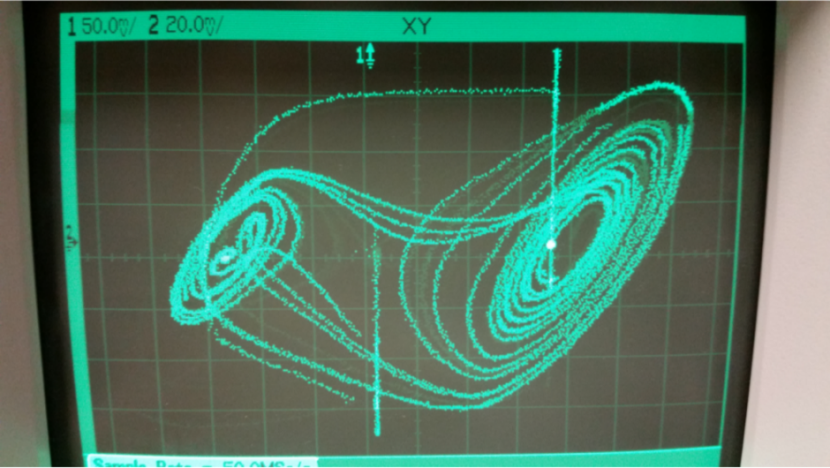
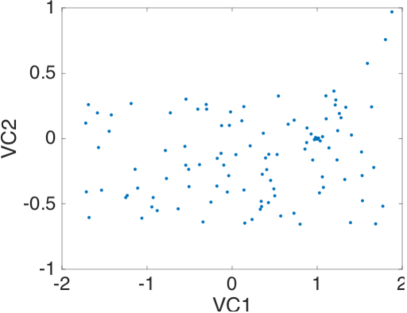
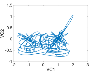
For the RSFF, we employ the same circuit frequency and perturbation on the initial conditions. This is plotted in Fig. 8(a). Moreover, in the circuit design, the outputs are achieved by taking the difference between the voltage across the capacitors and their respective threshold voltages. However, we approach this from the other direction where we have a model for the outputs and threshold voltages and take the sum to predict the voltage across the capacitors. Since our system is discrete and the phase plane of Chua’s circuit is continuous, we interpolate between the respective points. While this is not perfectly accurate, it illustrates a more complete picture of the dynamics than the purely discrete case. This is plotted in Fig. 8(b).
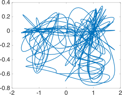
Again, as with the NOR gate, we are able to reproduce the behavior for the RSFF except for the clock edge effects. We also plot the iterate plane for the capacitor voltages. This can be thought of as iterates of a Poincaré map of the double scroll attractor. After interpolating between the iterates, we observe a double scroll like projection in the plane. However, it is not exactly a double scroll projection, nor can it be due to the artificial interpolation.
4 Stochastic model for set/reset flip-flop
4.1 Derivation
Now let us rectify the discrepancies between Figs. 7, 8(a) and Figs. 2, 3. Physically, the oscillations observed at certain clock edges are caused by a non-binary difference in the capacitor voltage and threshold voltage (recall that the outputs are calculated by subtracting the threshold voltage from the capacitor voltage). However, we take a different approach, developing a model for the threshold voltages and output voltages rather than determining the output voltages via the other two as explained in Sec. 3. In order to accomplish this, we must still rely on the physical intuition of the thresholding mechanism.
Whenever the inputs are such that they cause a threshold to change its state drastically (not including the gradual transition to chaos), the TCU attempts to synchronize the capacitor voltage with the threshold voltage for the proper output. This causes a competition between the capacitor voltage (under the influence of the previous input) and the TCU (stimulated by the current input), which the TCU finally wins. During this process, due to the chaotic nature of both the capacitor voltages and threshold voltages, each path to synchronization is different. Since we do not have the explicit model for the capacitor voltages, we will treat this competition as a stochastic process.
During the transitions that lead to the edge effect, we assume there is a probability at each time step that the output will either accept the new inputs or be induced by the weighted average of inputs from previous time steps, where the weights are also determined randomly (or rather, pseudo-randomly). Here we define time step as the reciprocal of the circuit frequency.
Consider the sequences , , and , such that and . Let be the number of time steps in the past that affect future outcomes and be the number of time steps after the edge that the output is affected (usually about millisecond). Further, let be the weights applied, with the same probability, out of , to the respective inputs, for . Let be some random variable for each time , with not necessarily identical distributions. In addition, let
| (11) |
be the perceived input. Then we substitute into (1) for the respective inputs,
| (12) |
to model the effects at the transition points. It should be noted that besides the transition points, which last about a millisecond, the outputs behave as described by the continuous extensions. Finally, In order to simulate noise produced by the wave generator, we add/subtract a small random term, , to the inputs (i.e. ).
4.2 Comparison with experiments
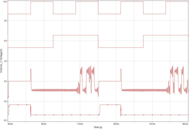
To simulate the models we use the same values for parameters in and , and for the circuit frequency, as Sec. 3.3. For the NOR gate and RSFF we set (i.e. approximately millisecond) and . The choice of describes a physical signal which has less than nano-volt of noise, on average. The simulations for the NOR gate are plotted in Fig. 9. We observe that these are precisely the type of damped oscillations seen in Fig. 2.
The RSFF and capacitor voltage simulations are plotted in Fig. 10(a) and 10(b) respectively. Observe that the oscillations match the type in Fig. 3(b). Furthermore, Fig. 10(b) is now qualitatively more similar to Fig. 2(b).
5 Conclusions
In the context of chaotic logical circuits there has been many SPICE simulations, some experiments, and only a few models. Simpler chaotic logical circuits are modeled as ordinary differential equations [3, 13]. More complex ones are generally studied using SPICE simulations [9, 10, 11] and physical realizations [9, 10]. We studied the RSFF/dual NOR gate through experiments, dynamical modeling, simulations, and analysis of the models.
By modifying the circuit in [11] we designed an RSFF/dual NOR gate using modern components. We then simulated the circuit using MultiSIM to confirm the new design produces the proper outputs. Next we put together a physical realization of the circuit and conducted experiments to show agreement with MultiSIM. By observing the behavior of the circuit and using properties of TCUs as seen in [9, 10] we are able to model the dynamics of the circuit as difference equations. The chaotic behavior of the models are verified by standard dynamical systems analysis for one-dimensional maps. Finally, we simulate our models to show agreement with both experiments and MultiSIM. It was expected that the original deterministic models would not be sufficient to replicate the “race” behavior observed in the outputs. Therefore, we inserted probabilistic elements to show this edge-trigger phenomenon, thereby deriving a stochastic model.
While we are able to capture much of the behavior, there is a need for more sophisticated models to replicate the more complex “race” behavior. Furthermore, as this is a rich problem, and we have a physical realization, many new phenomena may arise. It shall be useful to study various physical bifurcations as we make changes in the circuit and make connections with topological bifurcations. We predict this will lead to local bifurcations such as transcritical, pitchfork, and Neimark–Sacker as observed in other models [16, 18], and novel global bifurcations previously unobserved in the literature. We shall also endeavor to build other more complex circuits to study analogs of other logic families and exploit the chaotic and logical properties for the purposes of encryption and secure communication.
6 Acknowledgement
The authors would like to give their sincere thanks to the NJIT URI phase-2 student seed grant for funding this project. D. Blackmore and A. Rahman appreciates the support of DMS at NJIT, and I. Jordan appreciates the support of ECE at NJIT. The authors also thank Parth Sojitra for looking over the circuit when a bug was present.
References
- [1] L.M. Pecora and T.L. Carrol. Synchronization in chaotic systems. Phys. Rev. Lett., 64(8):821–824, 1990.
- [2] K.M. Cuomo and A.V. Oppenheim. Circuit implementation of synchronized chaos with applications to communications. Phys. Rev. Lett., 71(1):65–68, 1993.
- [3] H. Okazaki, H. Nakano, and T. Kawase. Chaotic and bifurcation behavior in an autonomous flip-flop circuit using piecewise linear tunnel diodes. Circ Syst, 3:291–297, 1998.
- [4] T. Matsumoto. A chaotic attractor from Chua’s circuit. IEEE Transactions on Circuits and Systems, CAS-31(12):1055–1058, December 1984.
- [5] M.P. Kennedy. Robust OP AMP realization of Chua’s circuit. Frequenz, 46:66–80, 1992.
- [6] L.O. Chua, C.W. Wu, A. Huang, and G.Q. Zhong. A universal circuit for studying and generating chaos - part II: Strange attractors. IEEE Trans. on Circuits and Systems, 40:745–761, 1993.
- [7] L.O. Chua. Chua’s circuit: Ten years later. IEICE Trans. Fundamentals, E77-A:1811–1821, 1994.
- [8] K. Murali and S. Sinha. Experimental realization of chaos control by thresholding. Phys. Rev. E, 68, 2003.
- [9] K. Murali, S. Sinha, and W. Ditto. Realization of the fundamental nor gate using a chaotic circuit. Phys. Rev. E, 68, 2003.
- [10] K. Murali, S. Sinha, and W. Ditto. Implementation of a nor gate by a chaotic Chua circuit. Int J Bifurcat Chaos, 13:2669–2672, 2003.
- [11] D. Cafagna and G. Grassi. Chaos-based SR flip-flop via Chua’s circuit. Int J Bifurcat Chaos, 16(5):1521–1526, 2006.
- [12] C Horsman, S Stepney, R.C. Wagner, and V Kendon. When does a physical system compute? Proc. Roy. Soc. A, 470(2169), 2014.
- [13] T. Kacprzak. Analysis of oscillatory metastable operation of RS flip-flop. IEEE J. Solid-State Circuits, 23:260–266, 1988.
- [14] D. Hamil, J. Deane, and D. Jeffries. Modeling of chaotic DC/DC converters by iterated nonlinear maps. IEEE Trans Power electronics, 7:25–36, 1992.
- [15] M. Ruzbehani, L. Zhou, and M. Wang. Bifurcation features in a DC/DC converter under current-mode control. Chaos, Solitons and Fractals, 28:205–212, 2006.
- [16] D. Blackmore, A. Rahman, and J. Shah. Discrete modeling and analysis of the r-s flip-flop circuit. Chaos, Solitons and Fractals, 42:951–963, 2009.
- [17] H.L.D. S. Cavalcante, Gauthier D.J., J.E.S. Socolar, and R. Zhang. On the origin of chaos in autonomous boolean networks. Phil. Trans. R. Soc. A, 368:495–513, 2010.
- [18] A. Rahman and D. Blackmore. Threshold voltage dynamics of chaotic rs flip-flop circuits. (Submitted, Preprint: Arxiv 1507.03065), 2016.
- [19] T.Y. Li and J.A. Yorke. Period three implies chaos. The American Mathematical Monthly, 82(10):985–992, 1975.
- [20] J. Guckenheimer and P. Holmes. Nonlinear Oscillations, Dynamical Systems, and Bifurcation of Vector Fields. Springer-Verlag, New York, NY, 1983.
- [21] R. Devaney. An Introduction to Chaotic Dynamical Systems. Benjamin/Cummings, 1986.
- [22] S. Strogatz. Nonlinear Dynamics and Chaos. Westview Press, Cambridge, MA, 1994.
- [23] C. Robinson. Dynamical Systems. CRC Press, 1995.
- [24] S. Wiggins. Introduction to Applied Nonlinear Dynamical Systems and Chaos. Springer-Verlag, New York, NY, 2 edition, 2003.
- [25] A. Marcovitz. Introduction to Logic Design. McGraw-Hill, New York, 2 edition, 2005.
Appendix A MultiSIM and Physical Realization
| Type | Quantity | Code | Comments |
|---|---|---|---|
| Resistor | 9 | ||
| Resistor | 14 | ||
| Resistor | 2 | ||
| Resistor | 2 | ||
| Resistor | 2 | ||
| Resistor | 1 | ||
| Resistor | 1 | ||
| Capacitor | 1 | ||
| Capacitor | 1 | ||
| Inductor | 1 | ||
| Op-Amp | 6 | AD713JN | Used only in MultiSIM |
| Op-Amp | 1 | LM759CP | Used only in MultiSIM |
| Op-Amp | 7 | NTE858m | Used only in physical realization |