Quantized transport, strain-induced perfectly conducting modes and valley filtering on shape-optimized graphene Corbino devices111This work has been published in Nano Letters on 4 August 2017, with the DOI 10.1021/acs.nanolett.7b01663.
Abstract
The extreme mechanical resilience of graphene 1, 2 and the peculiar coupling it hosts between lattice and electronic degrees of freedom 3, 4, 5 have spawned a strong impetus towards strain-engineered graphene where, on the one hand, strain augments the richness of its phenomenology and makes possible new concepts for electronic devices 6, 7 and, on the other hand, new and extreme physics might take place 8, 9, 10, 11, 12, 13, 14, 15. Here, we demonstrate that the shape of substrates supporting graphene sheets can be optimized for approachable experiments where strain-induced pseudomagnetic fields (PMF) can be tailored by pressure for directionally selective electronic transmission and pinching-off of current flow down to the quantum channel limit. The Corbino-type layout explored here furthermore allows filtering of charge carriers according to valley and current direction, which can be used to inject or collect valley-polarized currents, thus realizing one of the basic elements required for valleytronics. Our results are based on a framework developed to realistically determine the combination of strain, external parameters, and geometry optimally compatible with the target spatial profile of a desired physical property — the PMF in this case. Characteristic conductance profiles are analyzed through quantum transport calculations on large graphene devices having the optimal shape.
These authors contributed equally to this work. \altaffiliationThese authors contributed equally to this work. \alsoaffiliationCentre for Advanced 2D Materials, National University of Singapore, 6 Science Drive 2, Singapore 117546 \phone+65 6601 3642 \alsoaffiliationCentre for Advanced 2D Materials, National University of Singapore, 6 Science Drive 2, Singapore 117546
1 Introduction
An extremely active and promising area of research in strain-engineered two-dimensional electronic systems is the realization of graphene-based nanostructures with tailored pseudomagnetic fields (PMF). The PMF is a fruitful concept in strained graphene arising from the fact that, in the vicinity of the Dirac point, the description of the coupling between lattice deformations and electrons can be captured by two types of strain-induced fields: a displacement potential that couples to electrons as an electrostatic potential, and a strain-induced gauge field that couples similarly to a magnetic field 4. Since the former are expected to be effectively screened by the charge carriers, electrons are then expected to respond to strain mostly through this pseudomagnetic effect. Since (pseudo)magnetic fields are very effective means of guiding the motion and confining charged carriers, this naturally led to proposals and studies of many analogues of magnetic devices using graphene without actual magnetic fields, such as pseudomagnetic barriers 6, 16, 17, 18 or pseudomagnetic quantum dots 8, 19.
There are significant advantages of using pseudomagnetic fields in graphene electronic devices at the nanoscale. The first is that electrons in graphene are not easily confined by electric fields due to the Klein tunneling effect 20 arising from the relativistic-like behavior of electrons in this system. This has been a perennial difficulty and disadvantage of graphene-based electronics, while PMFs can efficiently localize electrons or act as tunneling barriers 6. The second advantage is that PMFs are only felt by the electrons in graphene, and they can be confined to regions as narrow as 5 – 10 nm 21, 12. This is unlike real magnetic fields which are felt not only by the target electronic system but also by whole the environment nearby. In addition, fabricating real magnetic barriers of nanoscale size is practically impossible and their magnetic field would also be fixed in principle, not reconfigurable or tuneable. Finally, the magnitude of PMFs that can be achieved in graphene is remarkably high and in excess of 300 T 21, 13, 12 which means that values of the order of tens of Tesla are easily obtainable, and strong enough for many electronic applications.
There is a key challenge that has persisted since the early proposals for strain-engineered graphene: the ability to tailor the spatial distribution of the PMF in graphene hinges on the ability to define specific non-uniform strain profiles, which is a difficult experimental prospect, especially at the micro and nanoscale. Moreover, whereas it is a straightforward theoretical task to start from a given strain field and determine the associated PMF and its impact in the electronic and transport properties, it is much less trivial and non-unique to request the opposite. Yet, it is precisely the opposite (i.e., specifying the PMF patterns in real space and obtaining the necessary strain profiles) that is of most direct interest for application in electronic devices because, in nearly any such case, one should be able to specify how, where, and to which extent we need electrons to be confined, which can be easily done reasoning in terms of PMF patterns alone, but is generally hard to anticipate in terms of strain alone. The central theoretical question for actual realizations and applications of strain-engineered graphene then becomes: how should one design the experimentally accessible parameters of the system (shape, external forces, constraints, substrate features, contacts, etc.) so that any given desired PMF pattern can be generated under realistic experimental circumstances?
In this work we pose and address one such question. We demonstrate that the geometry of a substrate can be optimized so that a graphene Corbino-type device can have its conductance suppressed when hydrostatically pressurized. This, on the one hand, can lead to extremely high on/off ratios due to the two contrasting transport regimes in the pressurized and relaxed states. Pressurized devices are shown to leak current only through perfect, spatially separated 1D modes arising from snake-type states that are stabilized at the inversion regions of the PMF. This creates a very strong current pinch-off by squeezing (literally in this case) the transport channel to the quantum wire limit and, in addition, establishes the possibility of having strictly quantized conductance on demand without electrostatic confinement. Moreover, since the chirality of PMF-induced snake states is uniquely tied to the valley degree of freedom, such devices can function as effective valley filters or sources of valley polarized currents. Our calculations are performed in an optimization framework that tackles the “reverse” strain-engineering problem in graphene. We begin with an overview of its main ingredients and a discussion of the optimal shapes for nearly uniform PMF throughout the Corbino ring. Subsequently, we describe how the deformation fields so obtained are mapped to an actual graphene lattice whose electronic properties are described in a non-uniform tight-binding approximation. This constitutes the basis for our study of the quantum transport characteristics and local electronic structure in devices of different dimensions, with and without disorder, whose results establish the behavior and phenomenology indicated above.
2 Corbino shape optimization
Stating the problem as an optimization question, we wish to find the shape of a non-circular annular cavity in a substrate such that the graphene flake, when deposited on it from above and subjected to hydrostatic pressure of magnitude , exhibits a pseudomagnetic field (PMF) with a magnitude that is constant in as much area of the system as possible, compatible with realistic elastic constraints. The substrate shape and dimensions so determined would constitute the basic information for the design of the corresponding transport experiment. If we assume that the graphene flake is rigidly attached to the substrate, finding the shape of the cavity is equivalent to finding the shape of the graphene flake with clamped boundary conditions at its edges, with the same optimized PMF under the applied hydrostatic pressure. This problem is solved by appealing to a Partial Differential Equation (PDE) constrained optimization technique, discretized by finite elements 22. It involves varying the control variables (the shape of the cavity) and the state variables (the plate deformation) so as to minimize a measure of the distance of the underlying PMF away from a certain desired PMF pattern, subject to the constraint that the state variables must satisfy the equations governing the elastic deformation of the graphene sheet for a given shape.
2.1 Overview of the inverse optimization problem
Our control variable is the shape of the domain occupied by the graphene flake (it is this that we numerically vary in order to approach the desired PMF in the pressurized field). We thus parametrize the domain using a set of control variables: , to be specified later. The clamped boundary conditions at the two perimeters (and beyond) where the graphene sheet contacts the substrate imply that the material domain of interest is the annular region defined by the patterning of the substrate, and not that part of the graphene that adheres to the substrate itself. The central mathematical problem is as follows:
| (1) |
subject to six constraint equations expressing the mechanical equilibrium of the graphene sheet, where the PMF is an explicit and known function of the strain field in the 2D sheet, and is the target PMF which, in general can be any predefined function of space. This formulation ensures that the sought in the optimization satisfies as closely as is feasible under the restrictions caused by the geometry and mechanics of the problem (the scheme seeks PMFs that are as close as possible to ; in the Supporting Information we discuss the case where the objective function is chosen to minimize , rather than ). represents the domain occupied by the unadhered part of the graphene flake, defined by a characteristic lengthscale . The explicit constraint equations that accompany eq. (1) are provided in the Supporting Information in order not to obscure the main discussion here. The final term is a regularization term necessary for well-posedness of the optimization problem. In reality, the optimization problem will be solved in dimensionless form but we present the dimensional version here for clarity.
2.2 Discretization and numerical solution
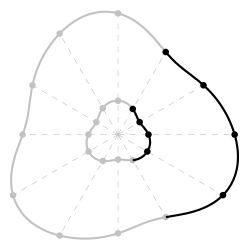
Each of the state variables (the three displacement components , , of the plate, and the three components of the bending moment , , ) is discretized using linear finite elements. This requires the generation of a triangular mesh covering the entire domain occupied by the graphene flake. However, the shape of this domain must be parametrized by a finite set of variables in order for the optimization algorithm (which works in a discrete setting) to be appropriately formulated. The simplest way to parametrize the shape of the domain is to prescribe equidistant control points around the outer and inner boundaries, and interpolate them with a Fourier series in the angular coordinate . Furthermore, due to the symmetry of the graphene lattice, the PMF is invariant if the coordinate axes are rotated by an angle of . Therefore we may restrict our domain to the region , and admit outlines of the form
| (2) |
only. An example of the domain construction from control points is shown in Figure 1. Let be the (even) number of control points on the outer boundary, with the same number on the inner boundary. Then if are the radial coordinates of the outer boundary for the angular coordinates , we have
| (3) |
where the coefficients are found by solving for . The same procedure is repeated for the inner boundary control variables . The control variables are allowed to vary within a user-provided interval,
| (4) |
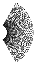
For each set of control variables chosen during the iterative optimization process, we will have a domain of a different shape. It would be improper to triangulate each new domain separately: not only would it be prohibitively time-consuming, but most optimization routines work best when the constraints and objective functions vary smoothly when the state and control variables are altered. Therefore, we instead choose a mesh for an annular sector and deform the mesh as the control variables accordingly alter the domain. The annular sector is defined by and , where
| (5) |
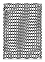
To mesh this annulus in a way which ensures a good resolution at the inner boundary, we construct a uniform mesh of points for the rectangle222A mesh size giving around 8 boundary elements per control point was used for the calculations in this article. Meshes were constructed using the Matlab-based mesh routine DistMesh 23.
| (6) |
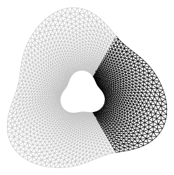
We conformally map the mesh for the rectangular domain to the annular sector using the mapping . Then, to deform this mesh to the domain defined by the control variables, we simply kept the -component of the meshpoint fixed, and affinely displaced the radial component to
| (7) |
where and its equivalent at the inner boundary are calculated from the control points by (3). See Figures 1–1 for a visualization of this procedure. The purpose of the regularization term in the objective function (1) is to make the optimization problem well-posed by penalizing solutions that have unfavorable properties. In this study we set the regularization function to be
| (8) |
in order to penalize highly-convoluted boundaries.
As discussed previously, the state variables are , , , , , , and are discretized such that the equations are written in terms of their values at each node in the triangulation. Additionally there are boundary conditions to be applied: the displacements are set to zero on nodes comprising the inner and outer boundaries. At the boundaries , we impose rotated periodicity conditions on these quantities (expressed in polar coordinates , ), i.e. , and similarly for , , , , . The discretized PDE system becomes a discrete optimization system: to minimize an objective function subject to constraints , where is the vector of control variables and is the vector of state variables.
3 Optimized device shapes
As the electronic and mechanical properties of graphene remain fixed, there are only three parameters that we can change in this system: the limits on the annulus shape (and hence the lengthscale ), the applied (constant) pressure , and the target PMF . In our calculations we allowed the outer control points to vary in a range and the inner points in a range . We initially set a target PMF of and the pressure was fixed at . Writing the coefficients to the nearest , the shape of the optimal outer and inner boundaries were calculated to be (in Angstroms)
| (9) | ||||
| (10) |
This outline corresponds to a striking flower-like geometry, and its deformation under hydrostatic pressure is displayed in Figure 2. To this deformation corresponds the spatial distribution of PMF shown in Figure 2. Though the target PMF was , the root-mean-squared value of the calculated PMF was only . It should be kept in mind that the target PMF is not in general attained in these optimization calculations, but is rather a mechanism for forcing the solution towards our desired direction.
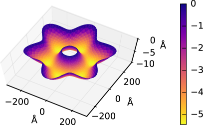
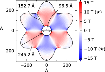
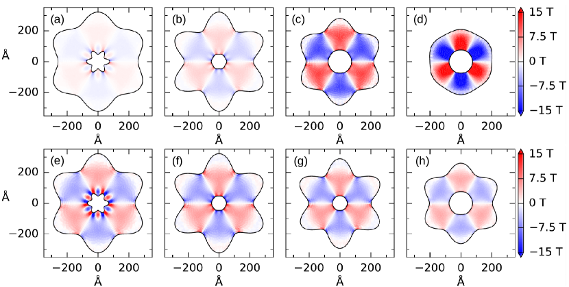
Since solutions to the optimization problem in eq. (1) are obtained for a specific choice of input parameters and , one immediate and important question is to assess how robust is the solution for the shape with respect to changes in those parameters. As the optimization and its constraints were solved in a dimensionless setting, the behavior of the solution is dependent on the values of dimensionless parameters rather than true physical quantities. The nondimensionalized system has only two parameters: the dimensionless bending stiffness , and the dimensionless pressure . In terms of the three physical quantities , , and , these parameters behave as (details in the Supporting Information)
| (11) |
Varying has little effect on the shape obtained through the optimization procedure (see Fig. S1 and related discussion in the Supporting Information), and so only changes in are relevant in understanding how the optimized shape depends on the choices of input parameters. For instance, increasing the hydrostatic pressure by a factor of and the target PMF by a factor of has no effect on the optimized shape, as the dimensionless constant is kept unchanged and the effect of a changed is negligible. In contrast, if is kept constant and is allowed to vary, we see a significant variation in the calculated shape as shown in Figures 3a–d. This variation in shape with changes in deserves further explanation. A change in corresponds to varying while keeping the lengthscale and target PMF constant. But a better way of seeing the effect is to think about an increase in as a decrease in target PMF , while keeping and constant [cf. eq. (11)]. Though this also changes the value of , we have noted that the effect of this is minor. To explore this line of thinking, in the lower row of Figure 3, we report a further set of calculations which kept and fixed while varying the target PMF through , , , and . For high target PMFs, the optimization forces the inner boundary to be highly convoluted in order to obtain the high strain gradients needed to achieve the target PMF. For low target PMFs, an annular solution is already close to the optimal solution, and the optimization only needs to make small adjustments to the outline to make the magnitude of the field more uniform. The results for and can be seen as intermediates between these two extremes. The two extremes also explain the results of Figure 3a–d calculated using different pressures for a given : for a low pressure, a convoluted interior boundary is required to hit the target PMF, while for high pressure an annular solution is already close to the target and only minor modifications of shape are needed. In the end, the two rows of Figure 3 illustrate what is implied by eq. (11): the changes in the optimal shape with increasing (and fixed ) follow the same trend as the changes with decreasing (and fixed ). Of the calculations shown in Figure 3e–h we selected the solution (g), which was shown before in Figure 2, with and as giving a good middle ground between PMF smoothness and strength.
If we are now given an arbitrary lengthscale and pressure , in order to find the optimal shape we need to choose an appropriate value of . Since we have seen that the result for gives an acceptable outcome, we could choose a that results in this value of . This gives us a system of equations with the same value of but a different value of as our first calculation. We have noted above that varying has little effect on the shape of the outline at constant . So, as long as the new value of does not fall too much beyond the range of magnitudes where we verified this to be true (supplementary Fig. S1), the solution will be similar to that in equations (9, 10), plotted in Figure 2. Since the differences are small, and would be dwarfed by manufacturing variability in a real system, we kept the same shape (9)–(10) in all our atomistic transport calculations to be discussed below for the sake of comparability. This shape is henceforth referred to as the flower device. The initial optimization was for a pressure of , and we performed further pressurizations of the shape up to , for which the distribution of PMF was not greatly changed, though its magnitude was quite different. Each of these pressurizations is identified below by the maximum strain achieved in the graphene sheet, up to a maximum strain of (note, however, that, even though our analysis is based on a set of specific parameter values, the scaling relations (11) allow the freedom to explore a large range of relevant pressures, target PMFs, or system sizes without having to run a new shape optimization procedure for each particular choice; see, for example, Fig. S6 in the Supporting Information).
4 Transport characteristics
To access the transport properties of the flower device we use the Landauer–Büttiker formalism; specifically, we are interested in the quantum conductance of the device, which is calculated by Caroli’s formula 24 , where is the retarded [advanced] Green’s function, the coupling between the contacts and the device is represented by , and is the self-energy of the contact . The geometry of the device is easily included in a nearest-neighbors -band tight-binding Hamiltonian by merely selecting the sites that are located between the mathematically defined inner and outer edges [cf. Figure 2]. The inner contact is essentially a circular contact with ; the outer contact radius varies between with the angular modulation prescribed by eq. (9). The calculation of the conductance requires the Green’s functions of these non traditional contacts; this problem can be resolved by recalling that, for graphene, the particular details of the contacts can be replaced by an effective self-energy term provided that the contacts inject a high number of modes (highly doped contacts) 25. Under this model, an effective self-energy term is added to the onsite energy of the atoms at the edges ( is the graphene hopping parameter).
The mechanical deformations induced by the hydrostatic pressure are incorporated in the tight binding Hamiltonian through the modification of the hopping parameter between neighboring sites as 26
| (12) |
where is the vector normal to the surface at point , is a vector linking the two sites, and and are the Slater–Koster parameters, modified to account for changes in the bond length through and 27, 28, 29.
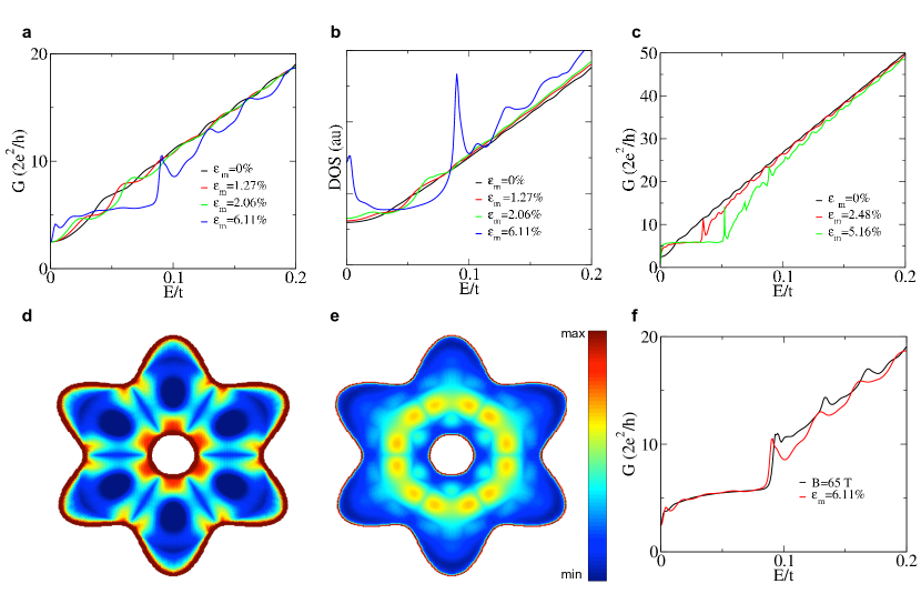
To best appreciate the features that arise from the pressure-induced PMF, it is useful, first, to have a perspective over the main transport characteristics of unpressurized devices which define our scenario of reference; the results of these calculations are provided in the Supporting Information. Devices were generated from the optimized flower shape shown in Figure 2 ( and ). Figure 4a shows the conductance of pressurized flower devices for different values of the maximal strain in the graphene flake, , that we use to distinguish different cases. Notably, at , the conductance starts developing a plateau of with a resonant peak at ; the plateau occupies the whole energy range . When the corresponding density of states (DOS) is analyzed [cf. Figure 4b], one identifies two sharp peaks at and arising from the formation of strain-induced LL with . From these, we extract a PMF and this estimate allows us to further confirm that local maxima occurring in the conductance of Figure 4a correlate to higher energy LL (, and ). The dependence of the conductance on device size for the same spatial distribution of PMF can be studied without having to run a new shape optimization procedure by exploring the scaling implied by eq. (11). For example, if one scales the inner and outer boundaries as , , these relations can be used to extract the pressure needed to achieve the same PMF pattern, as well as the magnitude of the quasi-uniform field (see Fig. S5 and related discussion in the Supporting Information). The conductance of a device thus scaled with () is shown in Figure 4c for maximal strains of and . In the two cases both the plateau and resonant peak are again present, from which we estimate and , respectively. However, in larger devices these features are much more sharply defined and the plateau is flatter: the conductance is therefore more perfectly quantized at with growing device dimension. They also require less strain to emerge due to the fact that the inner and outer contacts become decoupled at lower PMF (because the condition that the magnetic length, , is much less than is met at smaller PMF).
4.1 Perfectly conducting channels and valley filtering
In order to understand the origin of this robust quantization induced by pressure over a large range of energies that are experimentally relevant, let us look first at the real-space distribution of the electronic wavefunctions. The local DOS (LDOS) calculated at the plateau midpoint () and at the peak () are shown in Figures 4d and 4e, respectively, for the device with pressurized to [cf. Figure 4a]. At the peak [, Figure 4e], the observation of a state entirely confined in the central portions of the device identifies it as clearly associated with one of the PMF-induced LLs 19. In sharp contrast, for energies in the plateau [, Figure 4d] the LDOS concentrates on six narrow radial channels of the flower device. Comparing the LDOS with the PMF map shown in Figure 2 reveals that the wavefunction concentrates at precisely — and only — those regions where the PMF changes polarity. Consequently, the plateau in conductance at low energies is associated with current being carried by these pseudomagnetic interfacial states, similarly to the corresponding situation in nonuniform (real) magnetic fields 30 where electrons propagate chirally along a boundary separating fields of opposite polarity.
A useful picture of the nature of these 1D modes stabilized at the polarity inversion interfaces is provided by the semi-classical limit of this problem where they become so-called snake states 31. The designation arises from the different winding sense of the electron orbits in regions where has opposite polarity, which allows them to be confined and propagate along the interface with a definite direction. This interpretation helps one to understand: (i) directionality of the states and (ii) localization in regions where and changes sign. However, despite the usefulness of the semi-classical perspective, it is important to retain that no clear correspondence to the classical motion can be established in the case shown in Figure 4d because, as we are looking at energies between the and LL, the cyclotron radius is smaller than the magnetic length for the energies studied: 32, 33; these modes are in the quantum regime.
At low-energies, transport takes place via one-dimensional perfectly conducting modes, which is entirely consistent with the 1D-like energy dependence of the DOS plotted in Figure 4b for . Moreover, the six neighboring sectors of alternating PMF polarity in our flower device are expected to beget six snake state channels, so one may deduce the existence of a plateau in the conductance of , which is very approximately the case seen in Figures 4a and 4c. Note that, while one might think that the difference between the observed [] and theoretical values [] of the conductance plateau is due to the inhomogeneity of PMF over each sector, a direct comparison between the conductance of the pressurized device with an unpressurized flower under a real magnetic field with artificially sharp polarity changes shows no difference. More specifically, we have calculated the conductance of the same unpressurized device with an external magnetic field of constant magnitude () but alternating in sign at the six places where the PMF does so [cf. Figure 2 and Figure 5a] (additional details and different cases are discussed in the Supporting Information). Figure 4f demonstrates that the conductance of the pressurized device with is essentially the same as that of the idealized unpressurized device with real magnetic field of the same magnitude. The agreement is nearly perfect in the plateau region below the first LL, further corroborating that the flower device is the optimal solution (to emphasize this point, in the supplementary Fig. S4(e) we show that the conductance of pressurized annular devices that retain a perfectly circular shape does not develop the quantization plateau). It also validates our earlier argument regarding the origin of the chiral 1D channels in the pressurized devices and their close analogy to the semi-classical snake states. In the end, we can trace the small deviation from the ideal quantization in the pressurized devices of Figure 4a to a small coupling between the modes belonging to different radial segments: to avoid such coupling requires so that the wave functions of neighboring modes do not overlap near the inner contact, whereas this device has and which falls short of it. In the supplementary Fig. S4 we show that perfect quantization is indeed achieved when and fulfill that criterion and that, as expected more generally, the conductance step is quantized at , where is the number of polarity changing interfaces in the disk.
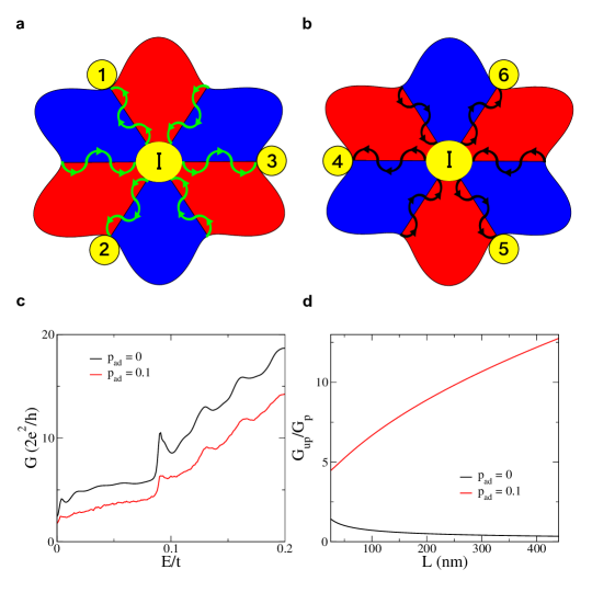
Given this scenario, the way in which PMFs couple to the electronic motion in graphene has an interesting and useful implication. Since electrons belonging to distinct valleys feel PMFs with opposite sign 4, 5, they propagate in opposite directions along the polarity boundary of the field. This effect is schematically illustrated in Figures 5a for an electron from valley , and 5b for valley . Looking back at Figure 4d, each radial segment along which the LDOS is peaked supports two chiral 1D modes, each propagating in opposite radial directions, and each associated with one given valley. Suppose then that the outer contact does not cover the entire perimeter but is, instead, sectioned into six outer contacts that allow collection of current only from the vicinity of the 1D channels (for our geometries that would mean defining contacts in the vicinity of the indentations of the outer perimeter, as in Figures 5a and 5b). Under a given bias between inner and outer contacts (say, electrons flowing radially outward), the electrons arising from valley would reach three specific contacts (all equivalent, oriented apart from each other), whereas those associated with valley would reach the other three contacts, as indicated in Figures 5a and 5b. In this schematic, electrons from valley are channeled by the 1D modes from the inner contact “I” to the outer contacts 1, 2 and 3, while those from valley can only reach contacts 4, 5 and 6. A change in the bias sign, or changing from electron to hole-doped graphene with a back gate, would exchange the valleys that “reach” a given contact. In this manner, the device can spatially separate individual contributions from each valley and deliver valley polarized current to specific contacts or, alternatively, selectively filter or probe the existence of valley polarized currents.
We highlight that the observation of these effects in our flower-like geometry is not limited to the specific range of hydrostatic pressure and device dimensions used for the calculations reported in Figure 5. For example, using the scaling relations (11), we expect that scaling up the device to while preserving its shape and using a pressure of shall create a PMF of with the same spatial distribution. The valley filtering effect will take place as long as LLs can be formed in the center of each petal guaranteeing that transport only takes place via the 1D modes. A simple estimate of the electronic mobilities needed for this can be made from the criterion that the mean free path, , be larger than the characteristic cyclotron diameter: . In terms of the mobility defined as and using for electrons in the first LL, this becomes , where we used ; such mobilities are rather standard in graphene devices (see Fig. S6 and related discussion in the Supporting Information for additional details).
Recent research has shown the existence of snake states in strained graphene nanoribbons PhysRevLett.112.096805, PhysRevB.94.075432, and diverse valley filtering devices have been proposed by exploiting strained graphene 34, 35, 36, 37, 38, 39. Similarly to ours, these devices require a specific geometry. However, ours does not require external electric or magnetic fields, produces valley filtered currents equally for both valleys, and whether the filtering occurs or not can be controlled by pressure or strain.
4.2 Effects of disorder and high on/off ratios
As often happens, disorder can simultaneously be detrimental or functional in solid state systems. From the first point of view, the conductance plateau associated with the snake states should be affected by disorder in real samples. As each radial channel supports one pair of opposite chirality and opposite valley quantum number, short-range scatterers will be particularly disadvantageous since they cause inter-valley scattering and, because of the valley-chirality locking, that translates into backscattering and the degradation of their perfectly conducting nature. Additionally, the snake states’ locations coincide with the sites of highest curvature in the pressurized flower where the probability of adsorbing alien atoms or molecules is higher 40, 41. In order to assess this in a specific manner, we modeled the attachment of adatoms to graphene in these regions by adding an Anderson-impurity type perturbation to the electronic Hamiltonian: each carbon can bind an adsorbate with probability ; this introduces a new electronic level of energy that the electron can hop to from the attached carbon with a hopping amplitude that describes the degree of hybridization 42. The conductance averaged over an ensemble of 20 such systems with for the device of Figure 4a is plotted in Figure 5c. As anticipated, the presence of these dopants in the regions where the snake states occur increases backscattering, thus lowering the conductance. The plateau is seen to remain, but its height depends inversely on the size of the system (not shown); in this particular case, traces of quantization are still present due to the small width of the device used (). We point out that the approximate preservation of the plateau under strong disorder (it affects 10 % of the atoms) is further evidence of the 1D character and resilience of the underlying modes: there is now backscattering (the plateau has smaller ), but the one-dimensionality is unaffected (a plateau largely remains).
Whereas such a system with strong short-range scattering will be less effective as a valley filter, the sensitivity of the low-energy base conductance to the radial dimension can have practical functional applications, as we now describe. Under pressure, the perfectly conducting channels limit the minimum conductance that can be achieved, irrespective of how large the magnitude of the PMF might be. From this standpoint, they are leaky electronic devices without an off state. But the residual conductance can be controlled by the type and amount of disorder, suggesting a tuneable on-off ratio. To simulate larger devices without incurring a high computational cost, and given that all of the above establishes the one-dimensional character of transport at low energies, we resort to a simple one-dimensional model 43 to scale up the conductance for larger pressurized disordered devices:
| (13) |
This assumes that in the snake-type 1D modes, electrons transmit through one adatom with probability and is the number of scatterers in the channel of width . It follows that wide devices should have a notorious reduction of the conductance, entailing high ratios of unpressurized/pressurized conductance () in the energy region of the snake states. This ratio can be used as a figure of merit directly related to the on-off ratio of the device. To quantify , we employed a number of modeling assumptions. Firstly, the Fermi energy was fixed at , corresponding to one half of the energy of the LL, the midpoint of the conductance plateau. Secondly, a perfectly round inner contact and ballistic transmission were considered in order to estimate , where is the maximum total angular momentum 25. Third, geometrical factors such as and were scaled from our original device (). Finally, the value was extracted from the disordered conductance of Figure 5c, from where we obtain . Figure 5d shows that, in pristine devices, decreases as . This decrease is due solely to because, in a clean device, remains at the value for any as long as . But, since the PMF scales inversely with for a fixed device shape, to keep this choice of requires its value to vary for different . Hence, each in the figure corresponds to a different , and these parameters vary inversely to each other; this causes the overall scaling shown by the black line in the figure. However, in the presence of the adsorbates, the 1D transport regime that occurs under pressure is expected to be much more sensitive to the disorder. The rapid decrease of the transmission probability with in this case dominates over the variation of . As a result, the figure of merit, which is governed by the overall transmission probability through , increases with the channel length reaching values near 12 for a device with (, ), a high “on/off” value considering the absence of a band gap in graphene.
5 Conclusions
In this work we set out to determine the optimal geometry of a graphene Corbino device that guarantees a PMF of nearly constant magnitude throughout most of the system when externally pressurized. Since the sign of the PMF has to inevitably alternate six times along any closed path containing the inner contact, the field cannot be strictly constant in the whole ring 8. Yet, both its magnitude and absolute value can be made satisfactorily uniform. The first case is discussed in the Supporting Information and we see that it is possible to require a specific sign and magnitude in most of the system, and the effect of the optimization process is to generate a geometry where the regions with the opposite PMF are much reduced (a more extreme spatial reduction is possible under higher pressures and higher target PMFs). If, on the other hand, the goal is only the PMF magnitude, but not its sign, the optimal geometries are the sixfold flower shapes such as in Figure 2 that we have analyzed in detail. The spatial boundaries where the PMF changes sign for the latter are sharper and better defined, which leads to robust snake states and strictly one-dimensional transport over a range of pressures. This radially one-dimensional regime is signaled by the strict quantization of the conductance at per channel that is seen to survive up to high values of (e.g. 50–100 meV, cf Figure 4), the characteristically 1D behavior of the DOS as a function of energy there, and corroborated by the real space profile of the LDOS.
The strain-induced perfectly conducting channels can be exploited in two different directions for electronic applications. On the one hand, they limit from below the current pinch-off effect and make these devices leaky because of their chiral nature. Our studies of the effect of disorder show that short-range defects can activate inter-valley scattering and reduce the residual conductance . Since their spatial location is set by the geometry, we can envisage this being done in a deliberate way through adsorbates, for example, so that only the regions where snake states develop under pressure become disordered. In this way, the conductance in the unpressurized state would remain unaffected, but the perfectly conducting channels would no longer exist under pressure which would significantly boost the on/off ratio. The pressure sensitivity and its direct translation into current modulations, suggests its possible application in electromechanical sensing or transducers 44. On the other hand, we have also seen an equally interesting perspective where snake-type states and their leaky residual conductance are not detrimental but, instead, functional: clean devices can be employed as sources of valley-polarized currents in graphene. Note that the Corbino ring (the device) is defined only by the indentation of the substrate, not by an actual patterning of graphene, and the inner and outer contacts at and are still the same sheet of graphene. Hence, the sheet can extend over large distances beyond the outer radius and these structures can act as local sources of valley-polarized currents for injection into the two dimensional graphene plane beyond .
DAB acknowledges the support from Mackpesquisa and FAPESP under grant 2012/50259-8, VMP that of the Singapore Ministry of Education Academic Research Fund Tier 2 under grant number MOE2015-T2-2-059, and AHCN the support of the National Research Foundation of Singapore under the Mid Size Centre Grant. Numerical computations were carried out at the HPC facilities of the NUS Centre for Advanced 2D Materials.
References
- Booth et al. 2008 Booth, T. J.; Blake, P.; Nair, R. R.; Jiang, D.; Hill, E. W.; Bangert, U.; Bleloch, A.; Gass, M.; Novoselov, K. S.; Katsnelson, M. I.; Geim, A. K. Nano Lett. 2008, 8, 2442
- Lee et al. 2008 Lee, C.; Wei, X.; Kysar, J. W.; Hone, J. Science 2008, 321, 385
- Kane and Mele 1997 Kane, C. L.; Mele, E. J. Phys. Rev. Lett. 1997, 78, 1932
- Suzuura and Ando 2002 Suzuura, H.; Ando, T. Phys. Rev. B 2002, 65, 235412
- Vozmediano et al. 2010 Vozmediano, M. A. H.; Katsnelson, M. I.; Guinea, F. Phys. Rep. 2010, 496, 109
- Pereira and Castro Neto 2009 Pereira, V. M.; Castro Neto, A. H. Phys. Rev. Lett. 2009, 103, 046801
- Tomori et al. 2011 Tomori, H.; Kanda, A.; Goto, H.; Ootuka, Y.; Tsukagoshi, K.; Moriyama, S.; Watanabe, E.; Tsuya, D. Appl. Phys. Express 2011, 4, 075102
- Guinea et al. 2009 Guinea, F.; Katsnelson, M. I.; Geim, A. K. Nat. Phys. 2009, 6, 30–33
- San-Jose et al. 2011 San-Jose, P.; González, J.; Guinea, F. Phys. Rev. Lett. 2011, 106, 045502
- Low et al. 2011 Low, T.; Guinea, F.; Katsnelson, M. I. Phys. Rev. B 2011, 83, 195436
- Wu et al. 2011 Wu, Z.; Zhai, F.; Peeters, F. M.; Xu, H. Q.; Chang, K. Phys. Rev. Lett. 2011, 106, 176802
- Klimov et al. 2012 Klimov, N. N.; Jung, S.; Zhu, S.; Li, T.; Wright, C. A.; Solares, S. D.; Newell, D. B.; Zhitenev, N. B.; Stroscio, J. A. Science 2012, 336, 1557
- Lu et al. 2012 Lu, J.; Castro Neto, A. H.; Loh, K. P. Nat. Commun. 2012, 3, 823
- de Juan et al. 2012 de Juan, F.; Sturla, M.; Vozmediano, M. A. H. Phys. Rev. Lett. 2012, 108, 227205
- Abanin and Pesin 2012 Abanin, D. A.; Pesin, D. A. Phys. Rev. Lett. 2012, 109, 066802
- Pellegrino et al. 2011 Pellegrino, F. M. D.; Angilella, G. G. N.; Pucci, R. Phys. Rev. B 2011, 84, 195404
- Bahamon and Pereira 2013 Bahamon, D. A.; Pereira, V. M. Phys. Rev. B 2013, 88, 195416
- Yesilyurt et al. 2016 Yesilyurt, C.; Tan, S. G.; Liang, G.; Jalil, M. B. A. AIP Adv. 2016, 6, 056303
- Qi et al. 2013 Qi, Z.; Bahamon, D. A.; Pereira, V. M.; Park, H. S.; Campbell, D. K.; Castro Neto, A. H. Nano Lett. 2013, 13, 2692–2697
- Katsnelson et al. 2006 Katsnelson, M. I.; Novoselov, K. S.; Geim, A. K. Nat. Phys. 2006, 2, 620
- Levy et al. 2010 Levy, N.; Burke, S. A.; Meaker, K. L.; Panlasigui, M.; Zettl, A.; Guinea, F.; Castro Neto, A. H.; Crommie, M. F. Science 2010, 329, 544–547
- Jones and Pereira 2014 Jones, G. W.; Pereira, V. M. New J. Phys. 2014, 16, 093044
- Persson and Strang 2004 Persson, P.-O.; Strang, G. SIAM Rev. 2004, 46, 329
- Meir and Wingreen 1992 Meir, Y.; Wingreen, N. S. Phys. Rev. Lett. 1992, 68, 2512–2515
- Bahamon et al. 2013 Bahamon, D. A.; Castro Neto, A. H.; Pereira, V. M. Phys. Rev. B 2013, 88, 235433
- Bahamon et al. 2016 Bahamon, D. A.; Qi, Z.; Park, H. S.; Pereira, V. M.; Campbell, D. K. Phys. Rev. B 2016, 93, 235408
- Tománek and Louie 1988 Tománek, D.; Louie, S. G. Phys. Rev. B 1988, 37, 8327–8336
- Pereira et al. 2009 Pereira, V. M.; Castro Neto, A. H.; Peres, N. M. R. Phys. Rev. B 2009, 80, 045401
- Yan et al. 2013 Yan, W.; He, W.-Y.; Chu, Z.-D.; Liu, M.; Meng, L.; Dou, R.-F.; Zhang, Y.; Liu, Z.; Nie, J.-C.; He, L. Nat. Commun. 2013, 4, 2159
- Park and Sim 2008 Park, S.; Sim, H.-S. Phys. Rev. B 2008, 77, 075433
- Müller 1992 Müller, J. E. Phys. Rev. Lett. 1992, 68, 385–388
- Rickhaus et al. 2015 Rickhaus, P.; Makk, P.; Liu, M.-H.; Tóvári, E.; Weiss, M.; Maurand, R.; Richter, K.; Schönenberger, C. Nat. Commun. 2015, 6, 6470
- Taychatanapat et al. 2015 Taychatanapat, T.; Tan, J. Y.; Yeo, Y.; Watanabe, K.; Taniguchi, T.; Özyilmaz, B. Nat. Commun. 2015, 6, 6093
- Carrillo-Bastos et al. 2016 Carrillo-Bastos, R.; León, C.; Faria, D.; Latgé, A.; Andrei, E. Y.; Sandler, N. Phys. Rev. B 2016, 94, 125422
- Low and Guinea 2010 Low, T.; Guinea, F. Nano Lett. 2010, 10, 3551–3554
- Gunlycke and White 2011 Gunlycke, D.; White, C. T. Phys. Rev. Lett. 2011, 106, 136806
- Fujita et al. 2010 Fujita, T.; Jalil, M. B. A.; Tan, S. G. Appl. Phys. Lett. 2010, 97, 043508
- Settnes et al. 2016 Settnes, M.; Power, S. R.; Brandbyge, M.; Jauho, A.-P. Phys. Rev. Lett. 2016, 117, 276801
- Milovanović and Peeters 2016 Milovanović, S. P.; Peeters, F. M. Appl. Phys. Lett. 2016, 109, 203108
- Geim 2009 Geim, A. K. Science 2009, 324, 1530–1534
- Cretu et al. 2010 Cretu, O.; Krasheninnikov, A. V.; Rodríguez-Manzo, J. A.; Sun, L.; Nieminen, R. M.; Banhart, F. Phys. Rev. Lett. 2010, 105, 196102
- Peres 2010 Peres, N. M. R. Rev. Mod. Phys. 2010, 82, 2673–2700
- Datta 1995 Datta, S. Electronic Transport in Mesoscopic Systems; Cambridge University Press, 1995
- Zhou and Zettl 2013 Zhou, Q.; Zettl, A. Appl. Phys. Lett. 2013, 102, 223109
See pages - of optimized_corbino_si.pdf\AtBeginShipout\AtBeginShipoutDiscard