Integrated optical force sensors using focusing photonic crystal arrays
Abstract
Mechanical oscillators are at the heart of many sensor applications. Recently several groups have developed oscillators that are probed optically, fabricated from high-stress silicon nitride films. They exhibit outstanding force sensitivities of a few aN/Hz1/2 and can also be made highly reflective, for efficient detection. The optical read-out usually requires complex experimental setups, including positioning stages and bulky cavities, making them impractical for real applications. In this paper we propose a novel way of building fully integrated all-optical force sensors based on low-loss silicon nitride mechanical resonators with a photonic crystal reflector. We can circumvent previous limitations in stability and complexity by simulating a suspended focusing photonic crystal, purely made of silicon nitride. Our design allows for an all integrated sensor, built out of a single block that integrates a full Fabry-Pérot cavity, without the need for assembly or alignment. The presented simulations will allow for a radical simplification of sensors based on high-Q silicon nitride membranes. Our results comprise, to the best of our knowledge, the first simulations of a focusing mirror made from a mechanically suspended flat membrane with subwavelength thickness. Cavity lengths between a few hundred m and mm should be directly realizable.
I Introduction
Over the past years, several designs of high-index contrast gratings have been investigated for various applications, like filters Boutami et al. (2006); Wang et al. (2015a, b), microcavities Li et al. (2011) or as planar alternatives to lenses Feng et al. (2005); Fattal et al. (2010); Lu et al. (2010); Zhan et al. (2016). Some of the designs feature membranes Letartre et al. (2003); Mateus et al. (2004) and even incorporate tunability of the focal length Kamali et al. (2016). At the same time, simultaneously designing and fabricating high reflectivity and good mechanical quality in an integrated MEMS structure has been a long outstanding goal. First realization of such devices have been made by patterning a diffraction grating into a silicon nitride membrane Stambaugh et al. (2015). Recently several groups have focused on using 2D photonic crystal arrays Crozier et al. (2006); Bui et al. (2012); Norte et al. (2016); Bernard et al. (2016); Chen et al. (2017), achieving reflectivities beyond 99%. Such devices are interesting for quantum optomechanics experiments, as they in principle allow for ground-state cooling from room temperature with potentially increased optomechanical coupling rates Xuereb et al. (2012). In order to combine the outstanding force sensitivity of these recent optomechanical designs Norte et al. (2016) with the capability of building a fully integrated optical sensor, it is very desirable to design and fabricate optical cavities directly on a chip. This avoids complex infrastructure for alignment and read-out and is inherently stable, opening up to possibility to use these sensors for easy to use, plug-and-play applications. Here, we present a design of a focusing 2D photonic crystal array, that avoids using several layers of dielectrics but can be directly patterned into a single sheet of material, like highly-stressed silicon nitride, which is known for its exceptionally low mechanical dissipation. This potentially allows the realization of a high quality mechanical system, necessary to achieve state-of-the-art force sensitivity, with a direct optical readout through a Fabry-Pérot cavity, all integrated on a single chip.
II Design approach
The general procedure to design our devices is as follows: we start with a two-dimensional photonic crystal (PC) slab – a thin, periodic photonic structure. Using Bloch’s theorem, the electro-magnetic (EM) waves in the slab can be decomposed into eigenmodes characterized by different bands and discrete wave vectors Joannopoulos et al. (2008). The profiles of the modes, and hence the optical properties of the slab, are governed by a single unit cell. By choosing a proper design of the unit cell an incoming mode can interfere destructively, resulting in high reflectance of the slab for a certain wavelength. In addition to controlling the amplitude reflectance, the wave also acquires a phase shift. Both the reflectivity and phase shift can be calculated using finite element method simulations with Floquet boundary conditions or rigorous coupled wave analysis (RCWA) Moharam and Gaylord (1981); Rumpf (2011), which can give modes and reflection properties at the same time.
In order to realize a focusing mirror, constructive interference of the reflected wave at the focal point is required. We can write the required profile of the phase shift on the reflector as
| (1) |
where is the wavelength, is the focal length, and is the location of a point on the reflector. is a constant phase shift that can be neglected. This gives rise to an ideal thin lens focusing Fattal et al. (2010); Lu et al. (2010). To calculate the focusing of the PC deterministically, a conventional PC is modified adiabatically such that it matches the target phase profile locally. A practical approach is to parameterize the geometry, and modulate the parameters of each single cell. Unavoidably, the periodicity is broken, however as is shown below, the structure can still retain high reflectivity, as has also been demonstrated in high-contrast photonic grating arrays Fattal et al. (2010); Lu et al. (2010); Klemm et al. (2013).
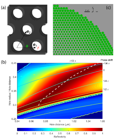
We start with an unmodulated PC, whose thickness and materials are determined by our optomechanical force-sensor design Norte et al. (2016) and ease of microfabrication. To fully define the basic unit cell we therefore have two parameters left that can be varied to match the desired phase shift and hence form a parameter space from which the whole pattern is generated. In principle, more degrees of freedom can be involved, but only at a significant increase in computational cost. We choose the air holes in our silicon nitride slab to form a hexagonal lattice as the basic shape (see Fig. 1), where the variables are distance between holes and filling factor, which is defined as the ratio of air hole radius to hole distance, . Then, using RCWA, we calculate the reflection amplitude of periodic PC in the parameter space, , giving the reflectivity and phase shift. The corresponding unit cells are building blocks of our focusing PC. We assume that is equal to the local reflection amplitude on the focusing PC, where a cell with parameters is located. Because both the target phase profile and the geometry of the structure vary adiabatically, these parameter values are taken from a smooth and continuous curve. Hence, the two parameters can be described by a single parameter, , where can be viewed as resulting from the parameterization of the curve.
Building a high finesse cavity to maximize the optical read-out sensitivity requires minimizing the optical losses, making a high reflectivity and large numerical aperture of the PC desirable. The latter is a consequence of the diffraction limit and is only important when the full range of a phase shift is not achievable. Therefore, we should restrict to being in an area of high reflectivity, while simultaneously maximizing the achievable phase shift they cover. In addition, considering the achievable accuracy in lithography, small fabrication errors should have a negligible impact on the phase profile. The procedure outlined above is repeated and optimized, where we vary the thickness and base shape of the design, until the requirements are fulfilled. The main challenges here are the moderate refractive index of SiN (), and the requirement of the membrane to be suspended, in order to achieve high mechanical quality factors. Note that previous devices with multi-layered materials Wang et al. (2015a, b) do not suffer from these limitations.
With a membrane thickness of 325 nm and for a laser wavelength of 1064 nm, we reach a maximum phase change of , and a continuous reflectivity of 86% (cf. Fig. 1(b)). This, however, does not give an upperbound for the reflectivity of the photonic crystal as a whole. Considering that the incident beam is a Gaussian wave, there is significantly more power concentrated in the center of the focusing PC, making the reflectance of the cells with smaller phase shift more important. Also, the reflectivity at the edge of the structure, which need large phase shift, suffers more from the edges of the structure, so the reflectance of the corresponding unit cell is less crucial. Hence, with our design, a reflectivity of 98% covers a phase change of , which is roughly the maximum achievable overall reflectivity. Also, increasing the size of the PC in general improves the reflectivity Chen et al. (2017).
Designing the full device now requires one last step: to put the cells into a plane layer. For that, we first specifiy the center cell. If all the chosen parameters are not able to cover a phase shift of full range, which is the case here, the phase profile of the center cell should be a maximum, which is an ending point of the curve. Then, all other cells are determined. In two dimension, we can label each cell by two numbers, . By matching the phase
| (2) |
a focusing PC is obtained. For an unmodulated PC, the location of a cell is , where are the primitive lattice vectors (), and we choose to be parallel to the axis. In a modulated structure, however is not well defined, since the photonic lattice is distorted. Still, considering that the structure is varied smoothly, can be approximated as a local vector using neighboring cells. Considering that the direction of should not change much, we use the scheme
| (3) |
where the factors and from the triangular lattice are retained. Since , combining with equation (2), and all undefined parameters for cell can be solved, given that cell and are already known. Therefore, all the cells can be determined in a systematic iterative process. In general, to determine one cell, two neighboring cells are related. At the beginning, only one cell is predefined. To solve this, the cells on the axis are found first. This then reduces to a scalar problem, while is always set. Due to the radial symmetry of the target phase and because the axis is a lattice axis, fixing these cells on the axis should not induce any error. We also predefine the cells along another lattice axis. Then, we settle the remaining cells. Part of the generated pattern is shown in Fig. 1(c), with a total radius of the PC of 30 m and a design focal length of 1000 m. Far away from the center, both the hole radius and distance are larger. Our final focusing PC design involves a change of between 0.97 to 1.05 m, while we sweep from 0.3 to 0.45. The exact path in this parameter space is shown in Fig. 1(b).
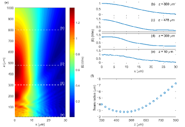
We finally simulate the full structure with a finite-difference time-domain method solver (FDTD, Lumerical) and the main result is shown in Fig. 2. Note that in general our simulations are done for TE polarized light. We however also verify that an optical TM mode yields the same results due to the symmetry of the PC. With an incoming Gaussian wave with radius of 18 m, we get a reflectivity of 96%, which is close to what we expect from the choice of cells, and a focusing efficiency of 98% Arbabi et al. (2015). The slightly lower reflectivity is primarily due to the power loss at the edge of the reflector. This can be be improved by increasing the size of the total PC – for example, by increasing the radius of 30 m to 45 m, the reflectivity increases to 97.5%. The main limitation here is the large increase in computational costs, as well as the desire to design a PC that fits onto our SiN tethered membrane oscillator, which has a lateral size of about 100 m. The particular choice of the beam waist is the optimum for the size of the PC, as a smaller waist would result in an increase in losses as it would sample less of the PC holes. With the beam waist centered on the reflector, the position at which the reflected wave is focused to a minimum is expected to be m, given by Saleh and Teich (1991)
| (4) |
Here is the Rayleigh range, and is the beam waist radius of the incoming wave. The deviation of from is a consequence of the long focal length and small beam waist. We are not able to simulate the electric field distribution as a function of distance directly in the FDTD solver because of its long and the resulting requirement in memory usage for the computation. Instead, we use Kirchhoff’s diffraction formula Guenther (1990) to generate Fig. 2(a)
| (5) |
where is a point on the reflector over which the integral is perform. We approximate the derivative by putting two monitors with a gap of 76 nm, which is the meshing precision in the direction. The resulting pattern shows a maximum of the electric field between 400 and 500 m away from the reflector. Far away from the optical axis, the electric field distribution cannot be approximated by a Gaussian, because of the finite size of the reflector. We fit the electric field for m using a Gaussian function to obtain the spot radius ( in intensity, cf. Fig. 2(b)-(e)) at different distances (Fig. 2(f)). The minimum of the beam spot is found to be around 475 m, close to ideal focusing. In our design process, we observe that each cell contributes to the local reflection amplitude, which is a discretization process. Even though the period of each unit cell, given by the hole distance ranging between 0.96 m and 1.06 m, is close to the optical wavelength, focusing still behaves as expected as small variations at short distance are averaged out far away from the reflector.
III Integrated optical sensors
One potential application for the mirror we designed could be in an optomechanical cavity, which is conventionally made of a highly-reflective membrane and a separate focusing mirror Gigan et al. (2006); Arcizet et al. (2006); Aspelmeyer et al. (2014); Reinhardt et al. (2016). While the mirror is fixed, the mechanical oscillation of the membrane is of great interest. Such a concept has been used to sense acceleration and other forces Krause et al. (2012); Metcalfe (2014); de Lépinay et al. (2016). To achieve high sensitivity, the optomechanical cavity should have a high optical quality factor. However, as the reflective membrane is usually small, any slight displacement of the membrane from the optical axis of the mirror greatly increases the loss, leading to a tedious alignment process usually involving sophisticated motorized stages. Such setups are bulky, complicated, expensive and inherently susceptible to vibrations. With our design method, we could use the focusing PC as an optomechanical cavity membrane, while at the same time focusing the optical beam onto a fixed, highly reflective mirror, that now can be part of a monolithic cavity (see Fig. 3(a)). The fixed mirror could for example be directly integrated as a distributed Bragg reflector, as already commonly used on chips in optomechanics experiments Gröblacher et al. (2009).
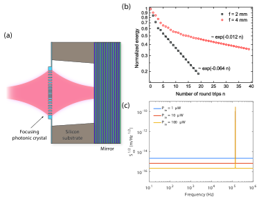
| Focal length | PC radius | Cavity length | Finesse |
|---|---|---|---|
| 1 mm | 29 m | 475 m | 56 |
| 2 mm | 41 m | 1 mm | 57 |
| 4 mm | 58 m | 1 mm | 103 |
One of the main limitation in our design are the cavity losses that result from the finite overlap of the optical mode and the membrane. Using equation (5) we can trace the intracavity field and, assuming a perfectly reflective membrane, calculate the resulting intensity decay rate. With a cavity length of 1 mm and focal length 2 mm, the loss per round trip is 6.4%, while for a focal length of 4 mm the losses can be reduced to 1.2% (Fig. 3(b)). Further increase of the focal length can result in even less losses and at the same time raises the membrane mass, while it adds difficulties in fabrication beyond practical limits due to the size of the membrane. With a phase shift of , the radius of the reflector is 58 m for a 4 mm focal length (see table 1). We will concentrate on this design, as the losses are already smaller than the loss on the membrane. Combining the two losses, the lower bound for the cavity finesse is estimated to be 103 (corresponding to a quality factor of ). We can now combine this design with our previously fabricated ultra-low mechanical loss membranes Norte et al. (2016). By modifying the pattern of the original reflector, a focusing PC can be realized in an otherwise almost unchanged silicon nitride membrane, resulting in a similar mechanical quality factor. We now use such a device as a model to analyze the performance of such a cavity sensor. Considering that the thickness is increased from 20 nm to 325 nm, the membrane is heavier, slightly reducing the sensitivity. Therefore, the intrinsic thermal noise of the mechanical oscillator is approx. m/Hz-1/2 at room temperature. In this cavity, the second, fixed mirror is assumed to be flat with a reflectivity of 99%. We calculate an achievable displacement sensitivity of m/Hz1/2 at 10 W, around one order of magnitude smaller than the standard quantum limit, while the force noise of the measurement can be expected to be below N/Hz1/2, if the transmitted power is measured by an ideal detector. With the modified mass being 16 ng, such a sensor would correspond to an accelerometer with a sensitivity of 54.6 g/Hz1/2, comparable to other recent optomechanics sensors Krause et al. (2012).
IV Conclusion
In summary, we describe a simple way of designing a stable, self-aligning optomechanical cavity, that should be able to have state-of-the-art force sensitivity. This is thanks to a novel single dielectric design using highly-stressed silicon nitride membranes, which are known to exhibit exceptional mechanical properties. We believe that such an integrated cavity could find applications both in precision measurements as well as in the field of optomechanics.
V Acknowledgements
We would like to thank João Moura for helpful discussions. This project was supported by the European Research Council (ERC StG Strong-Q, grant agreement 676842) and by the Netherlands Organisation for Scientific Research (NWO/OCW), as part of the Frontiers of Nanoscience program.
References
- Boutami et al. (2006) S. Boutami, B. B. Bakir, J.-L. Leclercq, X. Letartre, P. Rojo-Romeo, M. Garrigues, P. Viktorovitch, I. Sagnes, L. Legratiet, and M. Strassner, Opt. Express 14, 3129 (2006).
- Wang et al. (2015a) Y. Wang, D. Stellinga, A. B. Klemm, C. P. Reardon, and T. F. Krauss, IEEE J. Sel. Top. Quantum Electron. 21, 2700706 (2015a).
- Wang et al. (2015b) W. Wang, X. Gao, X. Fang, X. Li, H. Zhu, and Y. Wang, IEEE Photon. J. 8, 6800614 (2015b).
- Li et al. (2011) J. Li, D. Fattal, M. Fiorentino, and R. G. Beausoleil, Phys. Rev. Lett. 106, 193901 (2011).
- Feng et al. (2005) S. Feng, Z.-Y. Li, Z.-F. Feng, K. Ren, B.-Y. Cheng, and D.-Z. Zhang, J. Appl. Phys. 98, 063102 (2005).
- Fattal et al. (2010) D. Fattal, J. Li, Z. Peng, M. Fiorentino, and R. G. Beausoleil, Nature Photon. 4, 466 (2010).
- Lu et al. (2010) F. Lu, F. G. Sedgwick, V. Karagodsky, C. Chase, and C. J. Chang-Hasnain, Opt. Express 18, 12606 (2010).
- Zhan et al. (2016) A. Zhan, S. Colburn, R. Trivedi, T. K. Fryett, C. M. Dodson, and A. Majumdar, ACS Photonics 3, 209 (2016).
- Letartre et al. (2003) X. Letartre, J. Mouette, J. L. Leclercq, P. R. Romeo, C. Seassal, and P. Viktorovitch, J. Lightwave Technol. 21 (2003).
- Mateus et al. (2004) C. F. R. Mateus, M. C. Y. Huang, L. Chen, C. J. Chang-Hasnain, and Y. Suzuki, IEEE Photon. Technol. Lett. 16, 1676 (2004).
- Kamali et al. (2016) S. M. Kamali, E. Arbabi, A. Arbabi, Y. Horie, and A. Faraon, Laser Photonics Rev. 10, 1002 (2016).
- Stambaugh et al. (2015) C. Stambaugh, H. Xu, U. Kemiktarak, J. Taylor, and J. Lawall, Ann. Phys. 527, 81 (2015).
- Crozier et al. (2006) K. B. Crozier, V. Lousse, O. Kilic, S. Kim, S. Fan, and O. Solgaard, Phys. Rev. B 73, 115126 (2006).
- Bui et al. (2012) C. H. Bui, J. Zheng, S. W. Hoch, L. Y. T. Lee, J. G. E. Harris, and C. W. Wong, Appl. Phys. Lett. 100, 021110 (2012).
- Norte et al. (2016) R. A. Norte, J. P. Moura, and S. Gröblacher, Phys. Rev. Lett. 116, 147202 (2016).
- Bernard et al. (2016) S. Bernard, C. Reinhardt, V. Dumont, Y.-A. Peter, and J. C. Sankey, Opt. Lett. 41, 5624 (2016).
- Chen et al. (2017) X. Chen, C. Chardin, K. Makles, C. Caër, S. Chua, R. Braive, I. Robert-Philip, T. Briant, P.-F. Cohadon, A. Heidmann, et al., Light Sci. Appl. 6, e16190 (2017).
- Xuereb et al. (2012) A. Xuereb, C. Genes, and A. Dantan, Phys. Rev. Lett. 109, 223601 (2012).
- Joannopoulos et al. (2008) J. D. Joannopoulos, S. G. Johnson, J. N. Winn, and R. D. Meade, Photonic Crystals: Molding the Flow of Light (Second Edition) (Princeton University, 2008), 2nd ed.
- Moharam and Gaylord (1981) M. G. Moharam and T. K. Gaylord, J. Opt. Soc. Am. 71, 811 (1981).
- Rumpf (2011) R. C. Rumpf, Prog. Electromagn. Res. B 35, 241 (2011).
- Klemm et al. (2013) A. B. Klemm, D. Stellinga, E. R. Martins, L. Lewis, G. Huyet, L. O’Faolain, and T. F. Krauss, Opt. Lett. 38, 3410 (2013).
- Arbabi et al. (2015) A. Arbabi, Y. Horie, A. J. Ball, M. Bagheri, and A. Faraon, Nature Commun. 6, 7069 (2015).
- Saleh and Teich (1991) B. E. A. Saleh and M. C. Teich, Fundamentals of Photonics (John Wiley & Sons, Inc., 1991).
- Guenther (1990) B. D. Guenther, Modern Optics (Wiley, New York, 1990).
- Gigan et al. (2006) S. Gigan, H. R. Böhm, M. Paternostro, F. Blaser, G. Langer, J. B. Hertzberg, K. C. Schwab, D. Bäuerle, M. Aspelmeyer, and A. Zeilinger, Nature 444, 67 (2006).
- Arcizet et al. (2006) O. Arcizet, P.-F. Cohadon, T. Briant, M. Pinard, and A. Heidmann, Nature 444, 71 (2006).
- Aspelmeyer et al. (2014) M. Aspelmeyer, T. J. Kippenberg, and F. Marquardt, Rev. Mod. Phys. 86, 1391 (2014).
- Reinhardt et al. (2016) C. Reinhardt, T. Müller, A. Bourassa, and J. C. Sankey, Phys. Rev. X 6, 021001 (2016).
- Krause et al. (2012) A. G. Krause, M. Winger, T. D. Blasius, Q. Lin, and O. Painter, Nature Photon. 6, 768 (2012).
- Metcalfe (2014) M. Metcalfe, Appl. Phys. Rev. 1, 031105 (2014).
- de Lépinay et al. (2016) L. M. de Lépinay, B. Pigeau, B. Besga, P. Vincent, P. Poncharal, and O. Arcizet, Nature Nanotechnol. p. AOP (2016).
- Gröblacher et al. (2009) S. Gröblacher, J. B. Hertzberg, M. R. Vanner, S. Gigan, K. C. Schwab, and M. Aspelmeyer, Nature Phys. 5, 485 (2009).