Switchable valley filter based on a graphene - junction in a magnetic field
Abstract
Low-energy excitations in graphene exhibit relativistic properties due to the linear dispersion relation close to the Dirac points in the first Brillouin zone. Two of the Dirac points located at opposite corners of the first Brillouin zone can be chosen as inequivalent, representing a new valley degree of freedom, in addition to the charge and spin of an electron. Using the valley degree of freedom to encode information has attracted significant interest, both theoretically and experimentally, and gave rise to the field of valleytronics. We study a graphene - junction in a uniform out-of-plane magnetic field as a platform to generate and controllably manipulate the valley polarization of electrons. We show that by tuning the external potential giving rise to the - junction we can switch the current from one valley polarization to the other. We also consider the effect of different types of edge terminations and present a setup, where we can partition an incoming valley-unpolarized current into two branches of valley-polarized currents. The branching ratio can be chosen by changing the location of the - junction using a gate.
pacs:
81.05.ue, 73.40.-c, 73.43.-fI Introduction
Two-dimensional (2D) materials are promising candidates for future electronics due to their unique characteristics. The pioneering 2D material, graphene, was experimentally isolated in 2004 Novoselov2004 . The bandstructure of electrons in single-layer graphene, modeled as a honeycomb lattice with lattice constant nm consisting of two triangular Bravais sublattices and with nearest-neighbor hopping in the tight-binding formulation, hosts six Dirac cones resulting from touching of the valence and conduction bands at the Fermi energy . Two of the cones located at diagonally opposite corners of the first Brillouin zone can be chosen as inequivalent, for example at and . For the low-energy electronic excitations in the system they represent a new degree of freedom of an electron, in addition to the charge and spin. This valley degree of freedom can be exploited in analogy with the spin in spintronics, which gave rise to the field called valleytronics, where one uses the valley degree of freedom to encode information.
There is a strong motivation to generate, controllably manipulate and read out states of definite valley polarization, and a substantial amount of theoretical and experimental work has been done towards achieving these goals. A recent review of some advances made in the field of valleytronics in 2D materials is provided in Ref. Schaibley2016, . To mention some: a gated graphene quantum point contact with zigzag edges was proposed to function as a valley filter Rycerz2007 . Superconducting contacts were shown to enable the detection of the valley polarization in graphene Akhmerov2007 . In 2D honeycomb lattices with broken inversion symmetry, e.g. transition metal dichalcogenide (TMD) monolayers, a non-zero Berry curvature carries opposite signs in the and valleys. In these 2D materials, the velocity in the direction perpendicular to an applied in-plane electric field is proportional to this Berry curvature Xiao2010 . Hence the electrons acquire a valley-antisymmetric transverse velocity leading to the valley Hall effect, which spatially separates different valley states. In a system where the occupation numbers of the two valleys are different (valley-polarized system), a finite transverse voltage across the sample is developed and the sign of this voltage can be used to measure the valley polarization Xiao2007 . The valley Hall effect can also be exploited in a biased bilayer graphene, where the out-of-plane electric field breaks the inversion symmetry Li2016 ; Sui2015 ; Shimazaki2015 . Moreover, it was shown that the broken inversion symmetry results in the valley-dependent optical selection rule, which can be used to selectively excite carriers in the or valley via right or left circularly polarized light, respectively Yao2008 ; Xiao2012 . Valley polarization can also be achieved in monolayerPereira2009 ; Masir2011 ; Moldovan2012 ; Cheng2016 and bilayerCheng2016 graphene systems with barriers. In addition, proposals exploiting strain that induces pseudomagnetic fields acting oppositely in the two valleysMilovanovic2016 ; Settnes2016 together with artificially induced carrier mass and spin-orbit couplingGrujic2014 have been put forward.
In this paper we propose a way to generate and controllably manipulate the valley polarization of electrons in a graphene - junction in the presence of an out-of-plane magnetic field. Applying an out-of-plane magnetic field to the graphene sheet leads to the formation of low-energy relativistic Landau levels (LLs) Goerbig2011 . These are responsible for the unusual quantum Hall conductance quantization , where the integer is the highest occupied Landau level index (for -type doping) for a given chemical potential. The factor in the formula accounts for the spin degeneracy and the second factor for the valley degeneracy of the Landau levels. The presence of the Dirac point and particle-hole symmetry lead to a special LL, which is responsible for the fraction in the conductance.
Semiclassically, charged particles propagating in a spatially varying out-of-plane magnetic field in 2D may exhibit snake-like trajectories that are oriented perpendicularly to the field gradient Mueller1992 . The simplest case occurs along a nodal line of a spatially varying magnetic field Park2008 ; Oroszlany2008 ; Ghosh2008 ; Prada2010 . Another system, a graphene - junction in a homogeneous out-of-plane magnetic field, hosts similar states located at the interface between - and -doped regions. These interface states are also called snake states due to the shape of their semiclassical trajectories Carmier2010 ; Carmier2011 ; Rickhaus2015 . A correspondence between these two kinds of snake trajectories was pointed out in Ref. Beenakker2008a, . A mapping between these two systems was found by rewriting both problems in a Nambu (doubled) formulation Liu2015 . In this paper we consider a graphene - junction in a homogeneous out-of-plane magnetic field, a system which has attracted a lot of attention Cavalcante2016 ; Cohnitz2016 ; Fraessdorf2016 ; Kolasinski2016 ; Taychatanapat2015 ; Williams2007 ; Zarenia2013 . In the limit of a large junction (where the phase coherence is suppressed due to inelastic scattering or random time-dependent electric fields), the conductance is a series conductance of - and -doped regions Abanin2007 . However, for sufficiently small junctions the conductance depends on the microscopic edge termination close to the - interface. When the chemical potential in the and regions is within the first Landau gap, i.e., is restricted to energy values smaller than the absolute value of the energy difference between the zeroth and the first Landau level, an analytical formula for the conductance can be derived Tworzydlo2007 , see Eq. (2).
We demonstrate that a three-terminal device like the one shown in Fig. 1 can be used as a switchable, i.e. voltage-tunable valley filter. In short, it works as follows: valley-unpolarized electrons injected from the upper lead are collected in the lower leads with high valley polarization. The valley polarization of the collected electrons is controlled by switching the - junction on and off, while the partitioning of the electron density between the two lower leads is controlled by the edge termination and the width of the central region close to the - interface.
Our results are not restricted to graphene. They apply also to honeycomb lattices with broken inversion symmetry, where the inversion symmetry breaking term is represented by a staggered sublattice potential. As long as the amplitude of this term is smaller than the built-in potential step in the - junction, our results remain valid. In a system with broken inversion symmetry, a non-zero Berry curvature would give rise to the valley Hall effect which could be used to read out the polarization of the outgoing states Xiao2007 .
The rest of this article is organized as follows. In Sec. II we describe the setup of the proposed switchable valley filter and the methods we use to investigate its properties in detail. In Sec. III we present our numerical results, which demonstrate the valley-polarized electronic transport. In Sec. IV we study the effect of potential step height and different edge terminations of the graphene lattice close to the - interface on the valley polarization. We show that using a tilted staircase edge - junction allows to partition a valley-unpolarized incoming current into two outgoing currents with opposite valley polarizations, where the partitioning can be controlled by tuning the location of the - junction. Finally we summarize our results in Sec. V.
II Setup
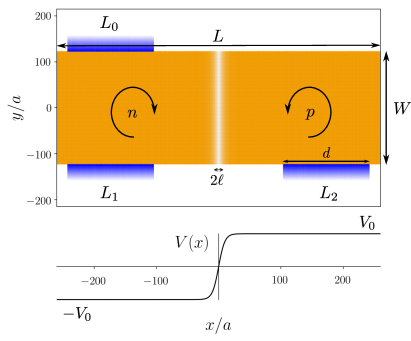
Figure 1 shows the three-terminal device that we would like to study. A rectangular region of width and length represents the graphene - junction in a uniform out-of-plane magnetic field, also referred to as the scattering region. It is described by a tight-binding Hamiltonian of the form
| (1) |
where is the scalar on-site potential at site with coordinate and is the Peierls phase accumulated along the link from site to site in magnetic field . The Zeeman splitting is neglected, i.e., we consider spinless electrons. The sum over denotes the sum over nearest neighbors.
We choose the Landau gauge, where the vector potential is
In this gauge we can define a (quasi-)momentum parallel to the edges of the leads. The leads , , and are modeled as semi-infinite zigzag nanoribbons, where the valley index can be well distinguished in -space. They are also described by the Hamiltonian (1) and below we present the case with in the leads, which is however not crucial for our results. The Peierls phase can be written in the form
where is the magnetic flux quantum and is the flux through a single hexagonal plaquette of a honeycomb lattice. Here, is the area of a hexagonal plaquette of the honeycomb lattice. An important length scale derived from magnetic field is the magnetic length . In the rest of the paper the magnetic field is chosen such that and hence . We also denote the energy difference between the first and the zeroth LL by , where the Fermi velocity at the point is .
The scalar on-site potential is varying only in the -direction as
where is the external scalar potential and is the thickness of the domain wall characterizing the - junction. If both and are non-zero and in such a setup, there exist two snake states co-propagating along the - junction Liu2015 . The orientation of the fields in the system is such that the snake states are traveling downwards in the negative -direction.
We calculate the transmission from to , and from to . We also calculate the valley-resolved transmissions, with the following notation: is the transmission from to , where in we sum only over outgoing modes with (). Then we can define the valley polarization in as . Analogous quantities are defined for .
Due to the absence of backscattering in chiral quantum Hall edge states and the symmetry of the - junction for , the net transmission (no spin) is , where is the highest occupied LL in the -doped region. The partitioning of the net transmission between and depends on the edge termination close to the - interface according to the formula Tworzydlo2007
| (2) |
where is the angle between valley isospins at the upper and lower edge represented as vectors on the Bloch sphere. For armchair edges one has if and otherwise. The formula is valid if the and regions are on the lowest Hall plateau, where the quantum Hall conductances in the - and -doped regions are equal to (ignoring the spin degree of freedom) Tworzydlo2007 . The transmission from to is then given by . Interference between wavefunctions of the snake states is responsible for this partitioning. The snake-state wavefunctions are located at the - interface and their effective spread in the -direction is given by the magnetic length to the left and right of the interface. Hence one way to control the partitioning experimentally will be to control the edge termination around the - interface on a length scale of the order of .
In the following we show numerically that by switching the - junction on () and off () we can control the valley polarization of the outgoing states in leads and .
III Switchable valley filter
We demonstrate the principle of the switchable valley filter using a - junction in an out-of-plane magnetic field, where the upper and the lower edges are of armchair type. The system is described by the Hamiltonian shown in Eq. (1). The width of the - junction is chosen such that the number of hexagons in this width is a multiple of , i.e. such that the corresponding armchair nanoribbon would be metallic. If, furthermore, both the - and -doped regions are on the lowest Hall plateau and is large enough Tworzydlo2007 , we expect and , see Eq. (2). The switchable valley filter is based on the fact that for a zigzag graphene nanoribbon the quantum Hall edge states of the LL lying in opposite valleys and have opposite velocities Brey2006 ; Beenakker2008b ; Goerbig2011 .
Unless stated otherwise, the system has length and width (the exception is Fig. 4). The horizontal size of each lead is . The thickness of the - junction is . We set the magnitude of the magnetic field in the leads to zero, which is however not crucial for the result. Our tight-binding calculations were performed using Kwant Groth2014 .
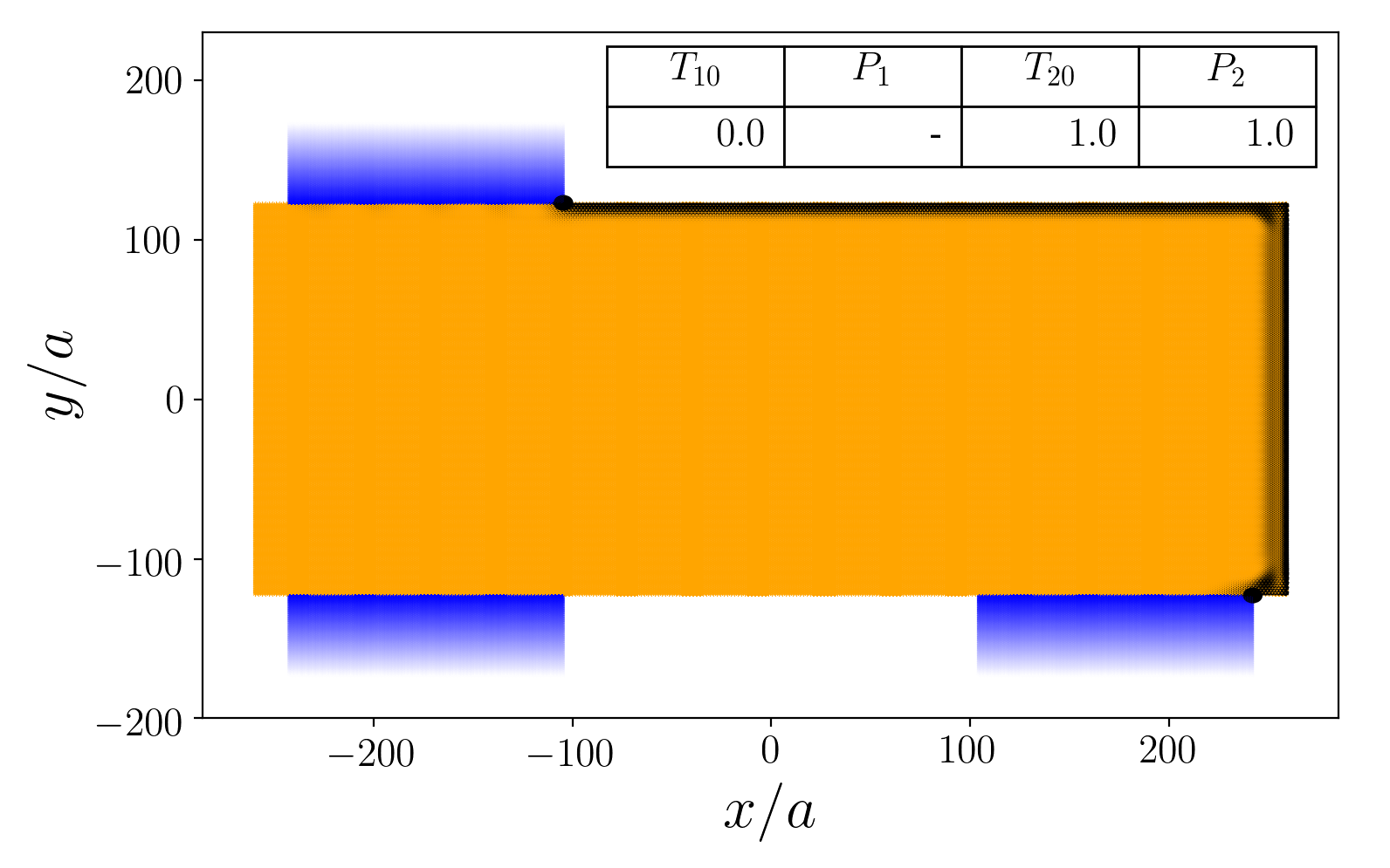
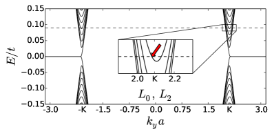
First, we consider the case . A valley-unpolarized electron current (injected from both valleys) in ends up as outgoing valley-polarized electron current in . In Figs. 2(a) and 3(a) we also plot the probability density of one of the states carrying the current by drawing a black dot on each site whose size is proportional to the probability of finding an electron on that particular site. This is plotted for a state in the scattering region due to an incoming mode from at Fermi energy and with momentum indicated by the red arrow in the bandstructure for , see Figs. 2(b) and 3(b). Figure 2(a) shows the probability density of the state in the scattering region due to an incoming mode from at and . Since , there are no snake states in this system and the electronic current is carried by the quantum Hall edge states. The electrons injected from travel in a clockwise manner to . The calculated transmissions and and polarizations and are shown in the inset table in Fig. 2(a). We find that the outgoing electrons in are perfectly polarized in the valley. This shows the valley-polarized nature of the zeroth LL. Thus, this system can be used as a valley filter.
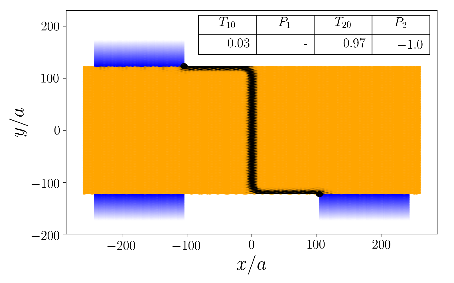
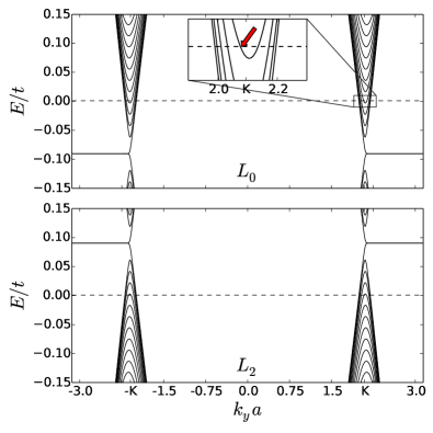
If we now turn on the - junction, the situation will change. We assume that the - junction is turned on adiabatically. We choose , so that the - and -doped regions are on the LL. Figure 3(a) shows the probability density of the state in the scattering region due to the incoming mode from at the Fermi energy and with (red arrow in the inset of Fig. 3(b)). In this system there are two co-propagating snake states along the - interface, and the electronic current is carried by these states. These snake states are located at the - interface and spread in the -direction over the magnetic length , which is independent of the domain wall thickness .
The electrons injected from now travel along the upper edge in the region towards the - interface and continue along the - interface towards the lower edge, where they enter the region with probability due to the specifically chosen and the armchair edge termination at both ends of the interface. Finally, they end up in . The corresponding transmissions and polarizations are shown in the inset table of Fig. 3(a). We find that the electrons in are nearly perfectly polarized in the valley. Thus, by turning on the - junction we have flipped the valley polarization of the electronic current in .
It is worth noting that these results are robust with respect to edge disorder because of the absence of backscattering in the chiral quantum Hall edge states. Our results also apply to the case where the magnetic field is present in the leads. However, since for low energies and dopings, only the LL plays a role, states in the leads are already valley-polarized edge states and thus our three-terminal device would then work as a perfect valley switch.
IV Polarizations and transmissions upon varying and geometry
In the following we analyze how the valley polarizations and and transmissions and change upon varying and edge terminations.
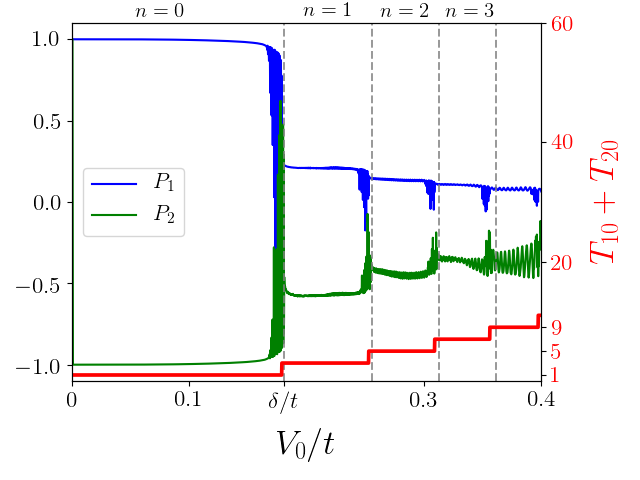
Polarization vs. . In Fig. 4 we plot the polarization in the leads as a function of . Let us focus on , because the majority of electrons are traveling into lead (for this specifically chosen scattering region). The case shown in Fig. 2 corresponds to , where (not visible in the figure). For (Fig. 3), the polarization in lead changes sign, . For only the LL valley-polarized edge states contribute to the transport and stays close to until . For the higher LLs get occupied. Edge states in the higher LLs are not valley-polarized which reduces . On further increasing higher and higher LLs get occupied which further obscures the edge state valley polarization of the LL and the magnitude of decreases. The population of the LLs can be seen from as a function of , which is shown with the red curve in Fig. 4. Hence the efficiency of the switchable valley filter device is observed to decrease with an increase in , i.e. with populating higher LLs.
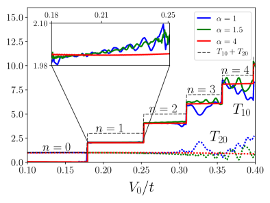
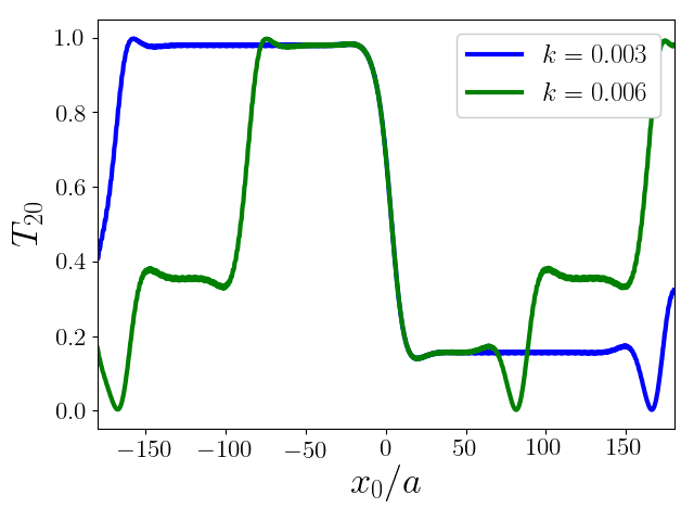
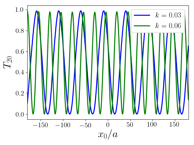
Furthermore, one can notice in Fig. 4 that the valley polarizations and in leads and jump at the same voltages , where the - junction undergoes quantum Hall transitions and the total transmission changes by . The larger , the more the values of at which the total transmission changes by 2 deviate from the vertical lines indicating the LL energies at . This is due to the nonlinearity of the dispersion which leads to a change in group velocity. The oscillations seen in the blue and green curves stem from oscillations of transmissions as shown in Fig. 5. This can be viewed as a consequence of interference effects between modes confined at the - interface with different momentaKolasinski2016 ; Milovanovic2014 . However, the amplitude of these oscillations decreases with increasing system size. In our simulations, the system size is increased proportionally, i.e. parameters and are multiplied by , while the magnetic flux per plaquette is kept constant, (see Fig. 5).
Different edge terminations. We find that different edge terminations and - interface length have almost no influence on the valley polarization in the leads, but they determine the partitioning of the net transmission between and . In Tab. 1(a), where the - interface meets armchair edges, and exhibit the expected periodicity when changing the width such that the number of hexagons across the width of the scattering region changes by . The case in which the - interface meets zigzag edges is considered in Tab. 1(b). Here, the transmissions and switch values depending on whether the two edges are in zigzag or anti-zigzag configuration, which is in agreement with Ref. Akhmerov2008, . To model different edge terminations, we also added a triangular region to the sample, see Tab. 1(c)–(e) (a zoom-in onto the tip is shown in the last column of Tab. 1(c)). Thus by controlling the edge termination on a length scale of around the - interface one can tune the partitioning of the current into and . The currents in both of these leads are polarized in opposite valleys. Thus if one chooses the situation where the current is finite in both and (for example the case shown in Tab. 1(c)), one can create two streams of oppositely valley-polarized currents in leads and .
| geometry | notes | ||||||||||||||||||||
|---|---|---|---|---|---|---|---|---|---|---|---|---|---|---|---|---|---|---|---|---|---|
| (a) |
|
|
|
|
|
||||||||||||||||
| (b) |
|
|
|
|
|
||||||||||||||||
| (c) | 0.48 | 1 | 0.52 | -1 | |||||||||||||||||
| (d) | 1 | 1 | 0 | – | W independent | ||||||||||||||||
| (e) | 0.02 | – | 0.98 | -1 | W independent |
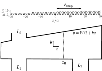
Tilted staircase edge. Now we consider the three-terminal setup shown in Fig. 6. The upper edge has many steps on the atomic scale, shown in the upper panel of Fig. 6. The size of each of these steps is assumed to be constant and is denoted by . The bottom-edge termination of the sample is of armchair type. We study the transmission as a function of the position of the - interface . Note that , because here the parameters are such that only the LL contributes to the electronic transport. If , the transmission shows a plateau-like behavior (see Fig. 7(a)). The transmission jumps to a different plateau as a new step is encountered while moving from to (the jump happens on length scales of the order of ). Since the upper and the lower edges are of armchair type, we observe three plateau values corresponding to different angles the between valley isospins at the two edges , in agreement with Ref. Tworzydlo2007, . The width of these plateaus corresponds to . In the regime there is a qualitative change from the plateau-like to sine-like behavior of , see Fig. 7(b). Thus, when , the incoming current in can be partitioned into valley-polarized currents in ( valley) and (- valley) in any desired ratio by tuning the location of the - junction. When , mixing of Landau orbits on neighboring guiding centers gives rise to the conductance behavior shown in Fig. 7(b). Our results are in agreement with the simulations in Ref. Handschin2017, .
In an experiment, one could measure the resulting valley polarization by utilizing the valley Hall effect Xiao2007 . This would require breaking the inversion symmetry, which can be modeled by a staggered sublattice potential of the form in our system. Our results remain valid even after adding such a term to the Hamiltonian in Eq. (1) as long as . This condition ensures the presence of snake states in the system at .
V Summary
In summary, we have demonstrated that a graphene - junction in a uniform out-of-plane magnetic field can effectively function as a switchable valley filter. The valley polarization of the carriers in the outgoing leads is quite robust. Changing the edge termination at the - interface can drastically modify the partitioning of the current into the two outgoing leads, but the outgoing current in both leads remains valley-polarized. We have also shown that in a device where one of the edges has many steps on the atomic scale, the partitioning of the current into two outgoing leads can be tuned by choosing the location of the - junction. In such a device it will be possible to partition a valley-unpolarized incoming current into two streams of oppositely valley-polarized currents in two outgoing leads in any desired ratio.
ACKNOWLEDGMENTS
We would like to acknowledge fruitful discussions with P. Makk, C. Handschin, and C. Schönenberger. This work was financially supported by the Swiss National Science Foundation (SNSF) and the NCCR Quantum Science and Technology. Work by EJM was supported by the Department of Energy, Office of Basic Energy Sciences under grant DE FG02 84ER45118.
References
- (1) K.S. Novoselov, A.K. Geim, S.V. Morozov, D. Jiang, Y. Zhang, S.V. Dubonos, I.V. Grigorieva, and A.A. Firsov, Science 306, 666 (2004).
- (2) J.R. Schaibley, H. Yu, G. Clark, P. Rivera, J.S. Ross, K.L. Seyler, W. Yao, and X. Xu, Nat. Rev. Mater. 1, 16055 (2016).
- (3) A. Rycerz, J. Tworzydlo, and C.W.J. Beenakker, Nat. Phys. 3, 172 (2007).
- (4) A.R. Akhmerov and C.W.J. Beenakker, Phys. Rev. Lett. 98, 157003 (2007).
- (5) D. Xiao, M.C. Chang, and Q. Niu, Rev. Mod. Phys. 82, 1959 (2010).
- (6) D. Xiao, W. Yao, and Q. Niu, Phys. Rev. Lett. 99, 236809 (2007).
- (7) J. Li, K. Wang, K.J. McFaul, Z. Zern, Y.F. Ren, K. Watanabe, T. Taniguchi, Z.H. Qiao, and J. Zhu, Nat. Nanotechnol. 11, 1060 (2016).
- (8) M. Sui, G. Chen, L. Ma, W. Shan, D. Tian, K. Watanabe, T. Taniguchi, X. Jin, W. Yao, D. Xiao, and Y. Zhang, Nat. Phys. 11, 1027 (2015).
- (9) Y. Shimazaki, M. Yamamoto, I.V. Borzenets, K. Watanabe, T. Taniguchi, and S. Tarucha, Nat. Phys. 11, 1032 (2015).
- (10) W. Yao, D. Xiao, and Q. Niu, Phys. Rev. B 77, 235406 (2008).
- (11) D. Xiao, G.B. Liu, W. Feng, X. Xu, and W. Yao, Phys. Rev. Lett. 108, 196802 (2012).
- (12) J.M. Pereira Jr., F.M. Peeters, R.N. Costa Filho, and G.A. Farias, J. Phys.: Condens. Matter 21, 045301 (2009).
- (13) M. Ramezani Masir, A. Matulis, and F. M. Peeters, Phys. Rev. B 84, 245413 (2011).
- (14) D. Moldovan, M. Ramezani Masir, L. Covaci, and F.M. Peeters, Phys. Rev. B 86, 115431 (2012).
- (15) S.-G. Cheng, J. Zhou, H. Jiang, and Q.-F. Sun, New Journal of Physics 18, 103024 (2016).
- (16) S. P. Milovanović and F. M. Peeters, App. Phys. Lett. 109, 203108 (2016).
- (17) M. Settnes, S. R. Power, M. Brandbyge, and A.-P. Jauho, Phys. Rev. Lett. 117, 276801 (2016).
- (18) Marko M. Grujic, Milan Ž. Tadić, and F.M. Peeters, Phys. Rev. Lett. 113, 046601 (2014).
- (19) M.O. Goerbig, Rev. Mod. Phys. 83, 1193 (2011).
- (20) J. E. Müller, Phys. Rev. Lett. 68, 385 (1992).
- (21) Sunghun Park and H.-S. Sim, Phys. Rev. B 77, 075433 (2008).
- (22) L. Oroszlány, P. Rakyta, A. Kormányos, C.J. Lambert, and J. Cserti, Phys. Rev. B 77, 081403(R) (2008).
- (23) T.K. Ghosh, A. De Martino, W. Häusler, L. Dell’Anna, and R. Egger, Phys. Rev. B 77, 081404(R) (2008).
- (24) E. Prada, P. San-Jose, and L. Brey, Phys. Rev. Lett. 105, 106802 (2010).
- (25) P. Carmier, C. Lewenkopf, and D. Ullmo, Phys. Rev. B 81, 241406(R) (2010).
- (26) P. Carmier, C. Lewenkopf, and D. Ullmo, Phys. Rev. B 84, 195428 (2011).
- (27) P. Rickhaus, P. Makk, M.H. Liu, E. Tóvári, M. Weiss, R. Maurand, K. Richter, and C. Schönenberger, Nat. Commun. 6, 6470 (2015).
- (28) C.W.J. Beenakker, A.R. Akhmerov, P. Recher, and J. Tworzydło, Phys. Rev. B 77, 075409 (2008).
- (29) Y. Liu, R.P. Tiwari, M. Brada, C. Bruder, F.V. Kusmartsev, and E.J. Mele, Phys. Rev. B 92, 235438 (2015).
- (30) J.R. Williams, L. DiCarlo, and C.M. Marcus, Science 317, 638 (2007).
- (31) M. Zarenia, J.M. Pereira, Jr., F.M. Peeters, and G.A. Farias, Phys. Rev. B 87, 035426 (2013).
- (32) T. Taychatanapat, J.Y. Tan, Y. Yeo, K. Watanabe, T. Taniguchi, and B. Özyilmaz, Nat. Commun. 6, 6093 (2015).
- (33) L.S. Cavalcante, A. Chaves, D.R. da Costa, G.A. Farias, and F.M. Peeters, Phys. Rev. B 94, 075432 (2016).
- (34) L. Cohnitz, A. De Martino, W. Häusler, and R. Egger, Phys. Rev. B 94, 165443 (2016).
- (35) C. Fräßdorf, L. Trifunovic, N. Bogdanoff, and P.W. Brouwer, Phys. Rev. B 94, 195439 (2016).
- (36) K. Kolasiński, A. Mreńca-Kolasińska, and B. Szafran, Phys. Rev. B 95, 045304 (2017).
- (37) D.A. Abanin and L.S. Levitov, Science 317, 641 (2007).
- (38) J. Tworzydło, I. Snyman, A.R. Akhmerov, and C.W.J. Beenakker, Phys. Rev. B 76, 035411 (2007).
- (39) L. Brey and H.A. Fertig, Phys. Rev. B 73, 195408 (2006).
- (40) C.W.J. Beenakker, Rev. Mod. Phys. 80, 1337 (2008).
- (41) C.W. Groth, M. Wimmer, A.R. Akhmerov, and X. Waintal, New J. Phys. 16, 063065 (2014).
- (42) S. P. Milovanović, M. Ramezani Masir, and F. M. Peeters, Appl. Phys. Lett. 105, 123507 (2014).
- (43) A.R. Akhmerov, J.H. Bardarson, A. Rycerz, and C.W.J. Beenakker, Phys. Rev. B 77, 205416 (2008).
- (44) C. Handschin, P. Makk, P. Rickhaus, R. Maurand, K. Watanabe, T. Taniguchi, K. Richter, M.-H. Liu, and C. Schönenberger, (unpublished).