Decoupling of graphene from Ni(111) via oxygen intercalation
Abstract
The combination of the surface science techniques (STM, XPS, ARPES) and density-functional theory calculations was used to study the decoupling of graphene from Ni(111) by oxygen intercalation. The formation of the antiferromagnetic (AFM) NiO layer at the interface between graphene and ferromagnetic (FM) Ni is found, where graphene protects the underlying AFM/FM sandwich system. It is found that graphene is fully decoupled in this system and strongly -doped via charge transfer with a position of the Dirac point of eV above the Fermi level. Our theoretical analysis confirms all experimental findings, addressing also the interface properties between graphene and AFM NiO.
I Introduction
Graphene (gr), a single layer of carbon atoms arranged in a honeycomb lattice, and its derivatives (flakes, quantum dots, nanoribbons, etc.) attract a lot of attention in the last decade due to its unique electrical and mechanical properties CastroNeto:2009 ; DasSarma:2011br ; Meunier:2016fr ; Si:2016dc . However, despite the tremendous success in the lab-based research, the lack of the “killer” graphene-based applications limits the spread of the graphene technology in our daily life Peplow:2015dd ; Park:2016ju . For example, implementation of graphene in the present-day scalable semiconducting technology requires its synthesis on insulating or semiconducting substrates. Presently this is only possible on h-BN Wang:2013do ; Tang:2013hy ; Tang:2015gn ; Driver:2016dx and Ge Wang:2013fq ; Lippert:2014fc ; Lee:2014dv ; Kiraly:2015kaa ; Dabrowski:2016im substrates at the conditions which cannot be easily adapted. Therefore, a new approach to synthesize the graphene/insulator systems was recently developed. It consists of the preparation of graphene on metallic or semiconducting layers via standard chemical vapour deposition (CVD) technique or intercalation under graphene, followed by the oxidation of the underlying metal or semiconductor at relatively high pressure of oxygen. This procedure was used in several recent works, where nearly free-standing graphene on bulk or surface oxide layers was prepared Larciprete:2012aaa ; Granas:2012cf ; Lizzit:2012hh ; Omiciuolo:2014dn ; Larciprete:2015ek ; Voloshina:2016jd .
This approach can also be used for the fabrication of graphene-protected systems Dedkov:2008d ; Dedkov:2008e ; Sutter:2010bx . Here as a first example one can consider the synthesis of the exchange biased epitaxial AFM/FM system under graphene, with AFM NiO and FM Ni having Neel and Curie transition temperatures well above the room temperature (AFM: antiferromagnet; FM: ferromagnet). The first attempt to prepare the graphene/NiO/Ni system was undertaken in Ref. 25 demonstrating the partial oxidation of Ni under graphene with formation of NiO islands at the interface. Neither structural nor electronic properties studies for the gr/NiO/Ni system can be found in the literature up to now.
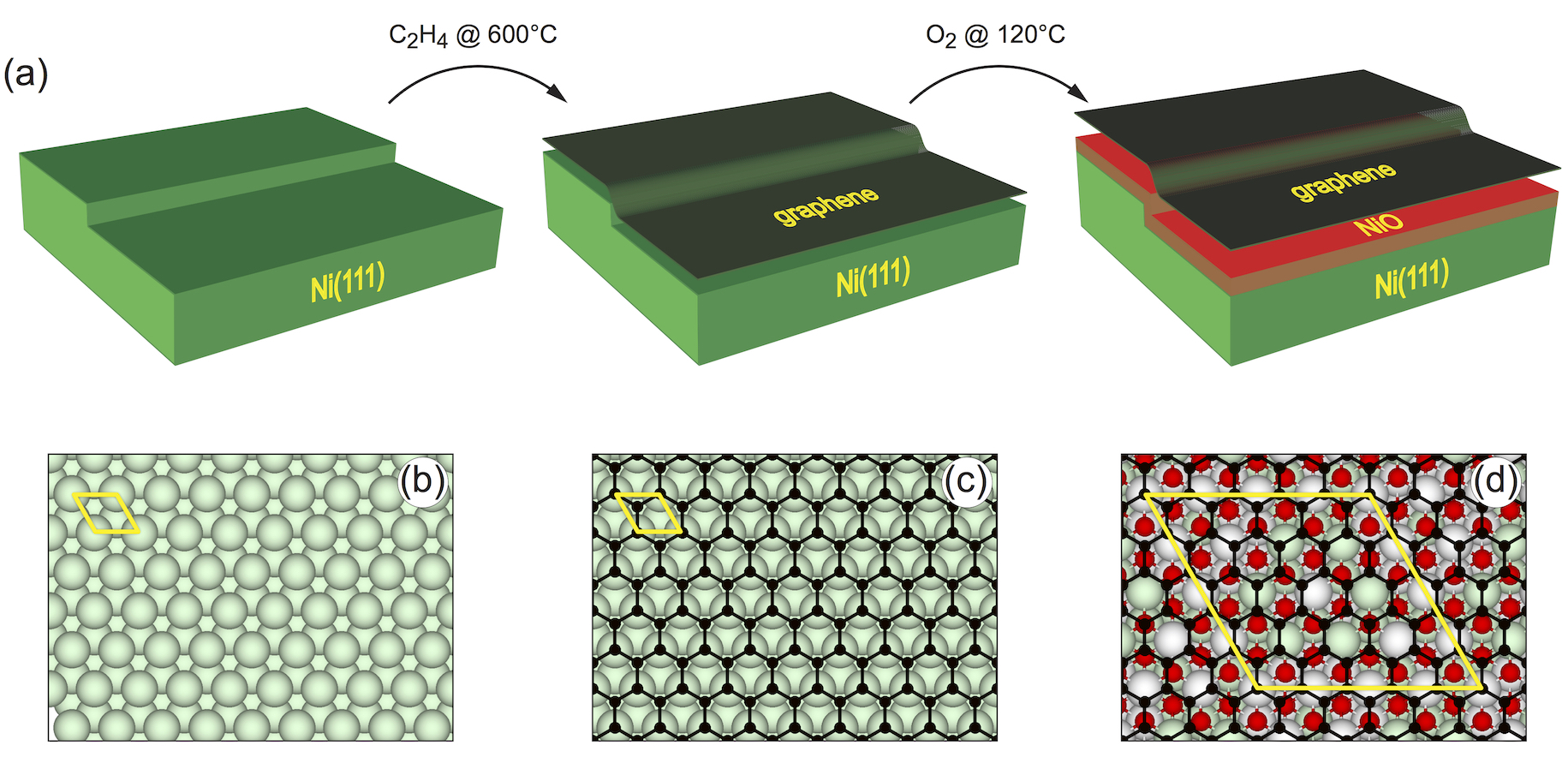
In the present paper we demonstrate successful complete intercalation of oxygen under graphene on Ni(111). We found that AFM NiO layer is formed at the interface between graphene and the FM Ni. The process of intercalation was monitored with scanning tunneling microscopy (STM) and x-ray photoelectron spectroscopy (XPS). Angle-resolved photoelectron spectroscopy (ARPES) experiments performed on graphene/NiO/Ni(111) showed that graphene is fully decoupled from the underlying substrate and strong -doping of graphene is found with a position of the Dirac point () of eV above the Fermi level (). All experimental results are analysed in the framework of the density-functional theory (DFT) approach and good agreement between experimental and theoretical data is found.
II Experimental and computational details
Experiments were performed in two different ultrahigh vacuum (UHV) systems (STM and XPS/ARPES) applying similar sample preparation conditions (Fig. 1). In both cases, the same Ni(111) single crystal was used as a substrate for graphene growth. Prior to every experiment, Ni(111) was cleaned via cycles of ion-sputtering (Ar+, eV, mbar, min) and annealing ( C, min). The cleanness of the surface was verified by means of LEED, STM, or XPS. Graphene was prepared in a usual way via low-pressure CVD procedure using ethene (C2H4) as a precursor ( C, mbar, min). This procedure gives a graphene layer of high-quality with a small fraction of the carbidic phase. The quality of graphene was verified by means of LEED, STM, and XPS/ARPES. Intercalation of oxygen in gr/Ni(111) was performed at C and oxygen was introduced through a stainless steel pipe which end was placed approximately mm from the sample surface, that allows to increase drastically the local pressure of oxygen at the sample position (approximately by 2 orders of magnitude). The partial pressure of oxygen in the preparation chamber measured by the hot-cathode ion gauge was mbar or mbar. The duration of this procedure determined the amount of intercalated oxygen; however, comparison with the preparations conditions which were used for oxygen intercalation in gr/Ru(0001) Voloshina:2016jd shows that for the formation of the fully decoupled layer of graphene on Ni(111) the oxygen dose has to be at least by factor of 10 higher compared to the former case. This difference is addressed in Sec. III.
All STM experiments were carried out in an UHV system (base pressure mbar) equipped with an Omicron variable-temperature scanning tunneling microscope. STM measurements were performed in the constant current mode at room temperature using electrochemically etched polycrystalline tungsten tips cleaned in UHV. The sign of the bias voltage corresponds to the voltage applied to the tip. Tunneling current and voltage are labeled and , respectively.
The XPS and ARPES experiments were performed at the UE 56/2 PGM 1 beamline at the BESSY II storage ring (HZB Berlin) in the photoemission station using PHOIBOS 100 2D-CCD hemispherical analyzer from SPECS GmbH. Photon energies are specified for every data set in the text and in the figure captions. In case of ARPES experiments a 5-axis motorized manipulator was used, allowing for a precise alignment of the sample in -space. The sample was pre-aligned (via polar and azimuth angles rotations) in such a way that the tilt scan was performed along the direction perpendicular to the direction of the graphene-derived BZ with the photoemission intensity on the channelplate images acquired along the direction. The final 3D data set of the photoemission intensity as a function of kinetic energy and two emission angles, , were then carefully analyzed.
Spin-polarised DFT calculations based on plane-wave basis sets of eV cutoff energy were performed with the Vienna ab initio simulation package (VASP) Kresse:1994 ; Kresse:1996a ; Kresse:1999 .The Perdew-Burke-Ernzerhof (PBE) exchange-correlation functional Perdew:1996 was employed. The electron-ion interaction was described within the projector augmented wave (PAW) method Blochl:1994 with Ni (, ), O (, ), and C (, ) states treated as valence states. The Brillouin-zone integration was performed on -centred symmetry reduced Monkhorst-Pack meshes using a Gaussian smearing with eV, except for the calculation of total energies. For those calculations, the tetrahedron method with Blöchl corrections Blochl:1994vg was used. A k-mesh was used in the case of ionic relaxation and for single point calculation, respectively. The DFT scheme Anisimov:1997gm ; Dudarev:1998vn was adopted for the treatment of Ni orbitals, with the parameter eV, which yields a band gap of eV for the bulk NiO, in good agreement with the experimental value, eV Sawatzky:1984jt . Dispersion interactions were considered adding a atom-atom term as parameterised by Grimme (“D2” parameterisation) Grimme:2006 .
For the calculation of the electronic properties of the gr/NiO(111) interface the O-terminated NiO(111) surface was modelled by a symmetric slab consisting of thirteen ionic layers. Graphene layers were adsorbed from both sides of the slab and a vacuum gap is approximately Å. The used supercell has a () lateral periodicity with respect to NiO(111) and a () lateral periodicity with respect to graphene. During the structural optimisation procedure the seven middle inner layers were fixed at their bulk positions whereas the positions of all other ions were fully relaxed until forces became smaller than . The band structures calculated for the studied systems were unfolded to the graphene () primitive unit cell according to the procedure described in Ref. 36 with the BandUP code. All calculations for gr/Ni(111) were performed according to procedure from Refs. 37; 38; 39.
III Results and discussions
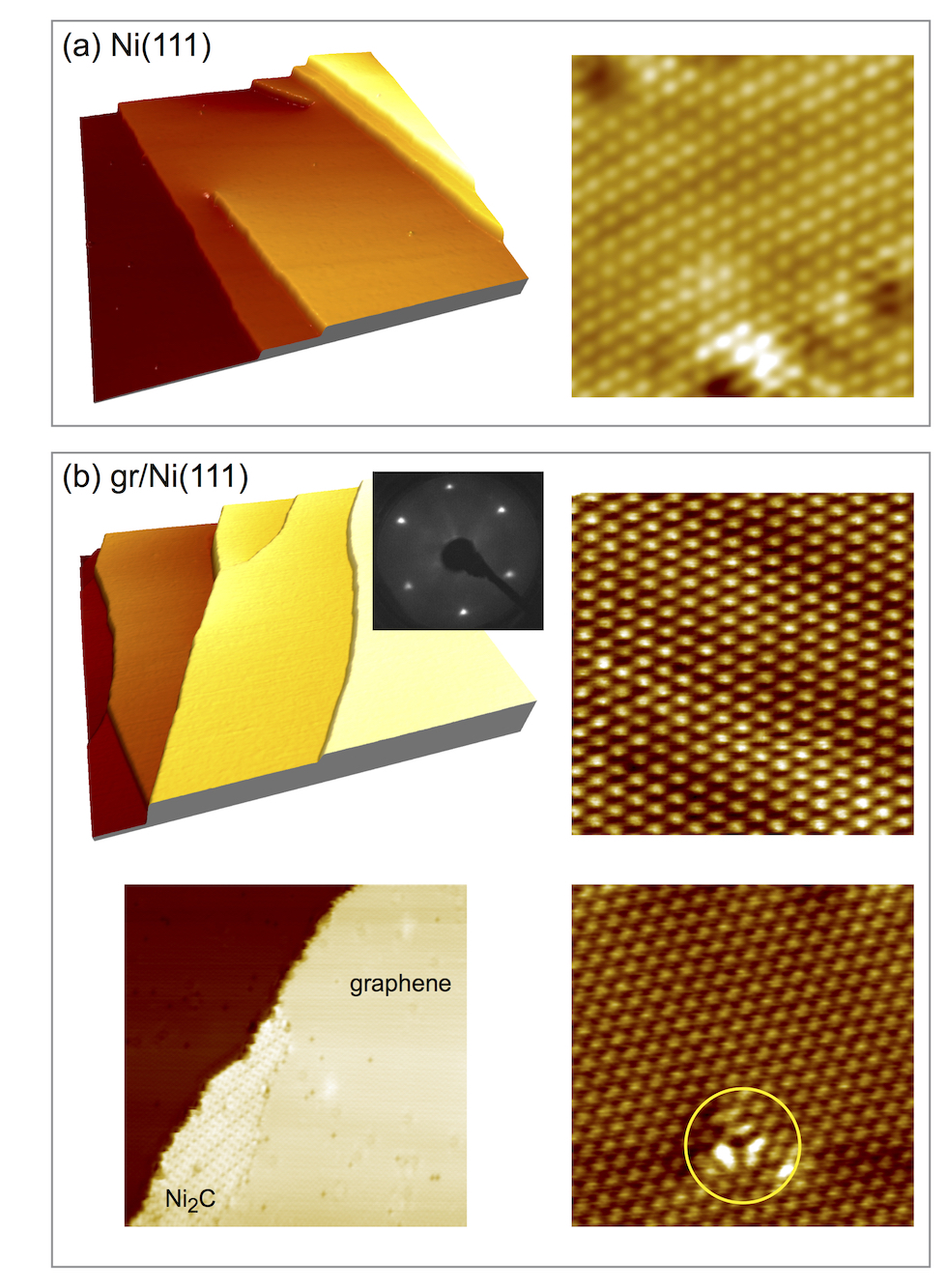
STM. Intercalation of oxygen in gr/Ni(111) and formation of the gr/NiO/Ni(111) system was verified using real-space STM as well as by spectroscopic methods. Figure 2(a) shows STM images of the clean Ni(111) surface, demonstrating ordered surface on the large (left) and small (right) scale. After preparation of graphene on Ni(111) [Fig. 2(b)], the large scale STM images show well ordered graphene layer with small fraction of the carbidic phase (Ni2C) Lahiri:2011iu ; Jacobson:2012be and very small number of single-atom vacancy defects Wang:2013jx . Two STM images showing such imperfections of the gr/Ni(111) system are presented in the bottom row of panel (b). These defected areas of the graphene layer (missing carbon atoms or/and borders between graphene and carbidic phases) can be considered as areas where intercalation of oxygen can take places. The high-quality of gr/Ni(111) is also confirmed by LEED images of this system, one of which is shown as an inset in Fig. 2(b). It is interesting to note that in our real-space STM experiments we observe the decrease of the number of screw-dislocations on the Ni(111) surface after preparation of a graphene layer, that can be assigned to the reduction of the surface (or interface) energy in the system and the respective atom rearrangement upon graphene formation.
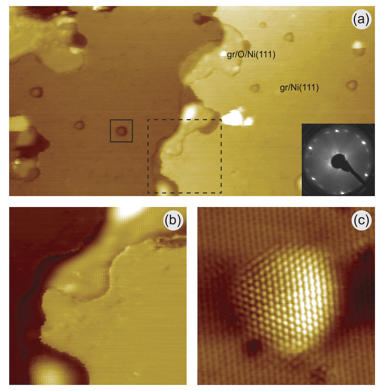
Intercalation of oxygen in gr/Ni(111) was performed at high partial pressure of gas and C. In order to trace the intercalation process and directly compare systems before and after intercalation, we present results for not fully decoupled graphene layer on Ni(111) (Fig. 3). Panel (a) shows a large scale STM image acquired after keeping gr/Ni(111) at C and mbar for min. After this procedure we can clearly discriminate between sample areas where oxygen was intercalated or not. It is interesting to note, that intercalation takes places mainly around step edges of the sample, where graphene might be partially lifted. Also several places on the terraces where oxygen intercalates in gr/Ni(111) and forms areas of the lifted graphene can be identified. The zoomed STM images of the step edge and the area on the terrace where intercalation takes place are shown in panels (b) and (c), respectively. Here we can conclude that intercalation of oxygen (and probably other species in the previous experiments reviewed in the literature) in graphene on metals takes places around extended or point defects in the graphene layer. For example one of such point defects is visible in the lower left part of image in panel (c). On other places, where graphene forms a perfect layer on the metallic substrate, it behaves as a protection carpet keeping the underlying metal surface intact.
XPS and TPD. In order to perform decoupling of the full graphene layer on Ni(111), much higher oxygen dose was used: C, mbar for min. Comparing the oxygen intercalation in gr/Ni(111) (present work) and in gr/Ru(0001) Voloshina:2016jd we can conclude that much higher oxygen dose is necessary in the former case. Such difference can be assigned to the different crystallographic structures of a graphene layer on metallic substrates. In case of gr/Ni(111), graphene forms a flat layer on a lattice matched Ni(111) surface with the distance to the top Ni layer of Å. For graphene on Ru(0001) a strongly buckled moiré structure is formed, due to the lattice mismatch between graphene and Ru lattices, where alternating places of the short ( Å) and long ( Å) C-Ru distances can be found. Such buckled structure with places of a locally lifted graphene might be easily intercalated by oxygen or other species, compared to flat gr/Ni(111), that is observed in our experiments.
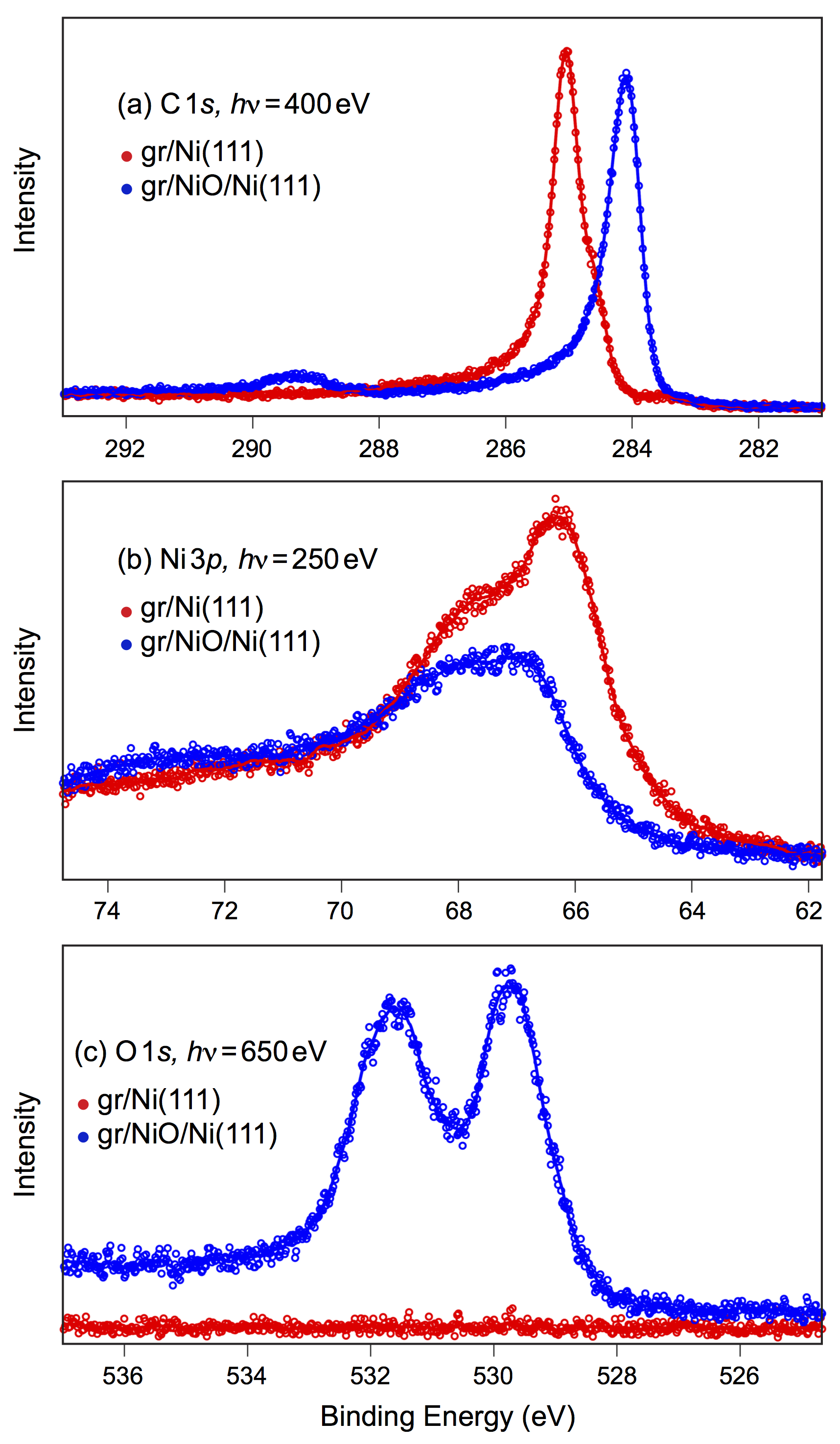
The chemical state of elements and the electronic structure of gr/Ni(111) and gr/NiOx/Ni(111) were studied by means of XPS and ARPES. Fig. 4 shows XPS spectra collected before and after intercalation of oxygen in gr/Ni(111). The C XPS spectrum of gr/Ni(111) [Fig. 4(a)] is in very good agreement with previously published data Dedkov:2008e ; Weser:2010 ; Voloshina:2011NJP ; Spath:2016db : the binding energy of this line is eV; the shoulder observed at the smaller binding energies can be assigned to the areas of gr/Ni(111) with implanted Ar atoms Spath:2016db (originates from the preparation procedure of the Ni crystal). The Ni XPS spectrum of gr/Ni(111) [Fig. 4(b)] shows a clear expected unmodified spin-orbit doublet.
The intercalation of the molecular oxygen in gr/Ni(111) at the conditions described earlier leads to the clear modifications of all XPS emission lines. The binding energy of the C line in the intercalation system is eV indicating the change of the doping level of graphene compared to the parent gr/Ni(111) system. In this case, we can expect the decoupling of the electronic states of graphene from those of the Ni(111) substrate due to the formation of the NiO layer at the interface. Absence of any residual XPS signal, which can be assigned to the gr/Ni(111) system, indicates the full decoupling of a graphene layer from the substrate and restoring of its nearly free-standing character. Intercalation of oxygen leads to the oxidation of the interface nickel and formation of the thin layer of NiO as can be deduced from the surface sensitive Ni XPS spectra of gr/NiO/Ni(111) [Fig. 4(b)], which shows a very good agreement with the data obtained for the bulk NiO (energy position as well as the satellite structure at larger binding energies) Sunding:2010gr .
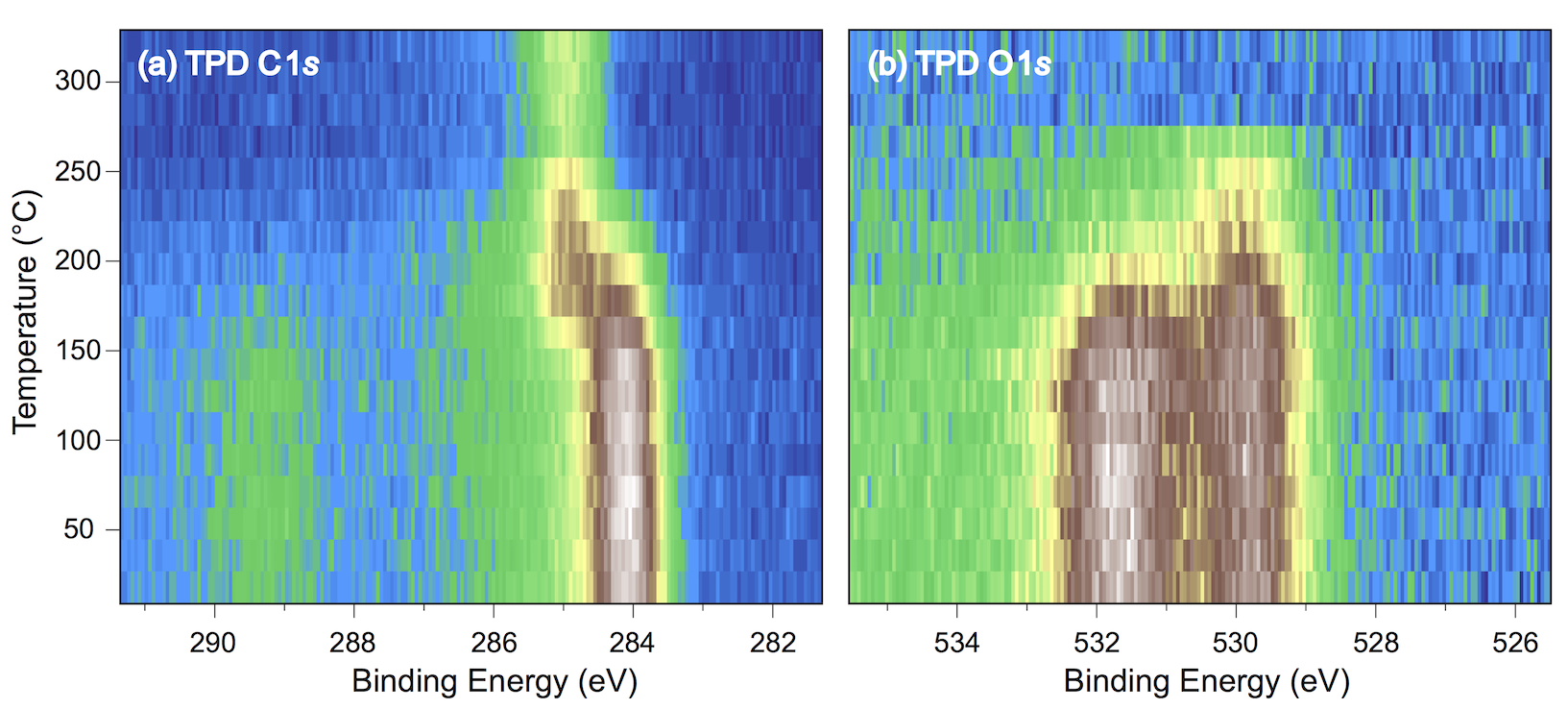
XPS measurements of the O line for the gr/NiO/Ni(111) system reveal two spectral components. The low binding energy component at eV can be clearly assigned to the emission from O2- in NiO Lorenz:2000cx ; Rettew:2011kd . The second one at eV might be due to the presence of the OH- groups on the surface Rettew:2011kd ; Tyuliev:1999je or can be connected with defects in the oxide layer Roberts:1984du . Our thermo-programmed desorption XPS (TPD-XPS) experiments performed for the C and O XPS lines (Fig. 5) suggest that higher binding energy O component is due to OH- groups. It is due to the fact that emission in the C line assigned to COOH-groups ( eV) Stankovich:2006dr and the discussed second component in the O line disappear simultaneously as the sample temperature approaches C. Further increase of the sample temperature leads to the “burning” of graphene via reaction of carbon atoms with oxygen from the NiO layer. Some weak C emission can still be detected, however, no complete layer of graphene can be observed (as concluded from the mesurement of very weak dispersion of the graphene bands in the ARPES experiments).
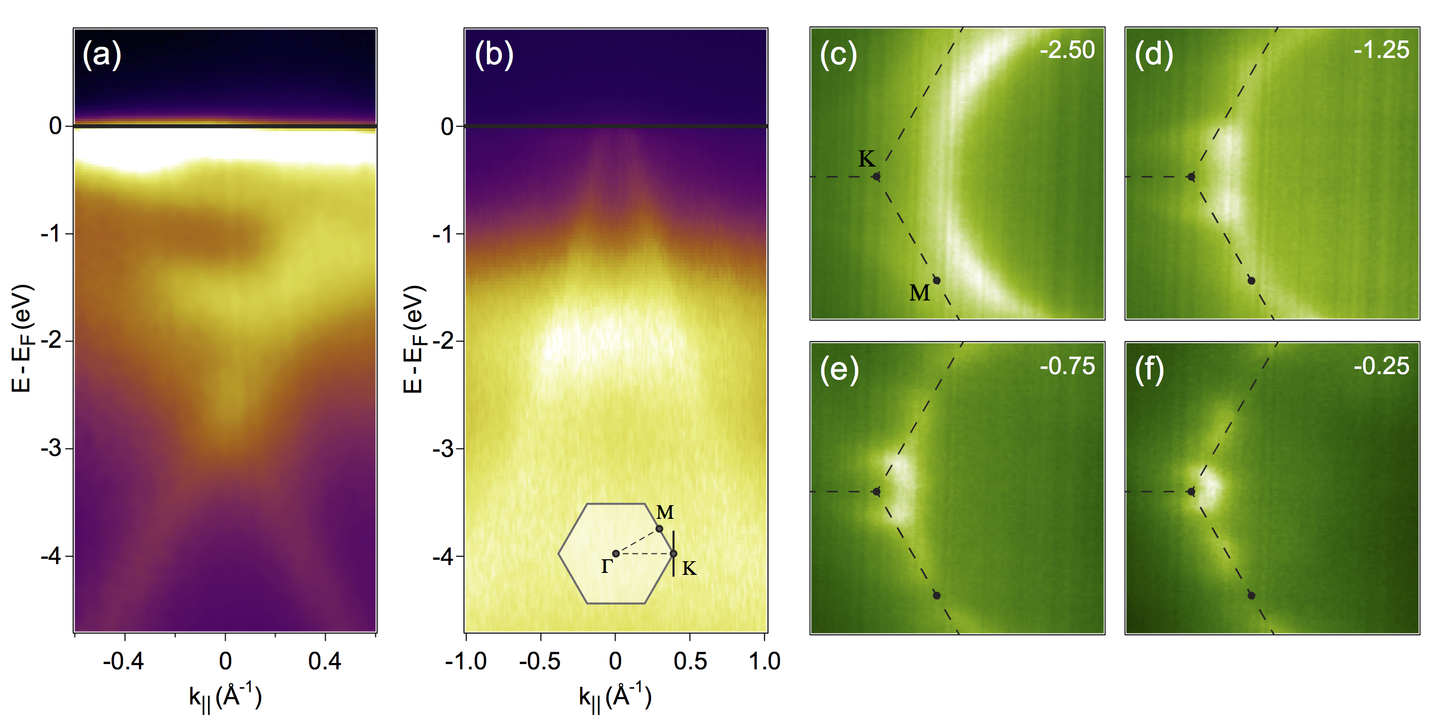
ARPES. Figure 6 compiles the results of our ARPES studies of gr/Ni(111) and gr/NiO/Ni(111). All images were extracted from the complete 3D data sets collected through the desired portions of the Brillouine zone of the studied systems. Panels (a) and (b) show the ARPES intensity maps for gr/Ni(111) and gr/NiO/Ni(111) as a function of the binding energy and the wave vector along the direction perpendicular to of the graphene Brillouine zone (marked by the solid line in the inset of (b)).
Considering the ARPES map of gr/Ni(111) (Fig. 6(a)), the strong modification of the electronic structure of a graphene layer is observed. As discussed in a series of previous works Voloshina:2011NJP ; Bertoni:2004 ; Dedkov:2010jh ; Voloshina:2014jl , the strong doping of a graphene layer and hybridization of the Ni and graphene valence band states lead to the shift of the graphene bands by eV below at the point, where a series of Ni -C hybrid states is formed. This effect leads to the strong redistribution of the valence band states in graphene and Ni and, e. g., induced magnetism in graphene layer was detected Weser:2010 , which was also later confirmed for other gr/FM interfaces Matsumoto:2013eu ; Weser:2011 ; Usachov:2015kr ; Marchenko:2015ka .
Intercalation of oxygen in gr/Ni(111) leads to the drastic changes in the observed ARPES picture [Fig. 6(b)]. The electronic structure of a graphene layer in the vicinity of is fully restored; graphene bands demonstrate linear dispersion; strong -doping of graphene is observed with a position of the Dirac point at eV. Valence band states of the underlying NiO having mainly Ni character are located at eV and eV. From the absence of the visible hybridization between graphene and NiO valence band states we can conclude that one of the conditions for this effect is broken, namely the space overlap of the Ni and C states. Therefore we can conclude that the NiO layer underneath graphene is terminated by oxygen.
Constant energy cuts extracted at different binding energies from the ARPES data set for gr/NiO/Ni(111) are shown in Fig. 6(c-f) (the respective binding energies are marked in every panel). The presented picture is characteristic for the free-standing graphene demonstrating a circular shape of the Fermi surface and clear trigonal warping of the band at high binding energies. These data demonstrate clear ARPES replicas which are rotated by with respect to the main bands and this observation correlates with the LEED spots observed for this system (inset of Fig. 3(a)), where additional LEED patterns are visible. This effect can be connected with the appearance of misoriented graphene areas due to the relatively large lattice mismatch between graphene and NiO(111) (see discussion below).
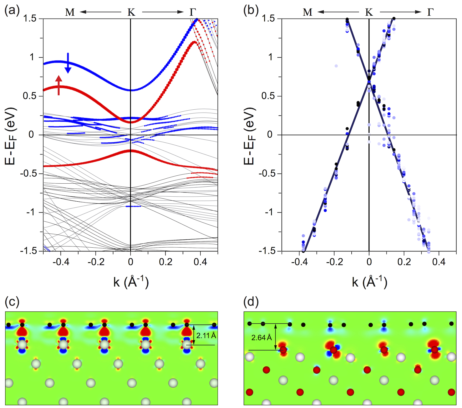
DFT. The electronic structure of gr/NiO(111)/Ni(111) was studied in the framework of the DFT approach. Structural optimizations show that graphene-substrate distance is increased from Å for gr/Ni(111) to Å for gr/NiO(111). As stated in Sec. II the band structure of the lattice-matched gr/Ni(111) interface was calculated for the unit cell and the one for gr/NiO(111) was calculated in the supercell geometry. The corresponding results are shown in Fig. 7 (a) and (b). The presented band structure for gr/Ni(111) is in perfect agreement with previously published data Voloshina:2011NJP ; Bertoni:2004 ; Voloshina:2014jl ; Weser:2011 , where one can clearly see that the original band structure of graphene is fully destroyed and a series of the hybrid Ni-C interface states is formed.
After oxygen intercalation in gr/Ni(111), a thin layer of NiO is formed underneath graphene and this layer is oxygen terminated. Therefore in our DFT calculations graphene was placed on the O-terminated NiO(111) slab in the supercell geometry. The resulting band structure of graphene in this system, which was unfolded on the unit cell of graphene is shown in Fig. 7 (b). [The plotted discrete band structure is due to the unfolding procedure and complicated unit cell of the gr/NiO(111) interface.] The restoring of the original linear dispersion of the states in the band structure of the free-standing-like graphene layer is clearly visible. Our DFT calculations show that graphene in the gr/NiO system is strongly -doped with the position of the Dirac point at eV, that is in a very good agreement with the value extracted from the experimental data. The effect of decoupling of graphene from the substrate after oxygen intercalation is also demonstrated in Fig. 7 (c) and (d), where electron density difference is presented for gr/Ni(111) and gr/NiO(111), respectively. In agreement with the band structures one can see that in the former case the strong hybridization between Ni and graphene states is observed. In case of the gr/NiO(111) interface, a graphene layer is fully decoupled from the substrate and only the effect of the charge transfer, i. e. the -doping of graphene, is observed.
IV Conclusions
In our work we demonstrate the successful intercalation of molecular oxygen in gr/Ni(111) and formation of a graphene-protected AFM/FM system. This process leads to the formation of a thin NiO layer as deduced from our experimental data. In the gr/NiO interface, a graphene layer is fully decoupled from the substrate, demonstrating nearly free-standing character. The effect of adsorption of graphene on NiO leads to the -doping of graphene with the position of the Dirac point of eV above the Fermi level. All experimental results are confirmed by state-of-the-art DFT calculations demonstrating very good agreement between all data.
Acknowledgement
We thank HZB for the allocation of synchrotron radiation beamtime. F.S. and C.P. thank the German Research Foundation (DFG) for funding through SFB 953 “Synthetic Carbon Allotropes” and the Cluster of Excellence “Engineering of Advanced Materials”. E.V. thanks DFG for financial support within the Priority Programme SPP 1459 “Graphene” and the North-German Supercomputing Alliance (HLRN) for providing computer time.
References
- (1) A. Castro Neto, F. Guinea, N. Peres, K. Novoselov, A. Geim, The electronic properties of graphene, Rev. Mod. Phys. 81 (2009) 109–162.
- (2) S. Das Sarma, S. Adam, E. H. Hwang, E. Rossi, Electronic transport in two-dimensional graphene, Rev. Mod. Phys. 83 (2011) 407–470.
- (3) V. Meunier, A. G. Souza Filho, E. B. Barros, M. S. Dresselhaus, Physical properties of low-dimensional -based carbon nanostructures, Rev. Mod. Phys. 88 (2016) 025005–50.
- (4) C. Si, Z. Sun, F. Liu, Strain engineering of graphene: a review, Nanoscale 8 (2016) 3207–3217.
- (5) M. Peplow, Graphene booms in factories but lacks a killer app, Nature 522 (2015) 268–269.
- (6) S. Park, The puzzle of graphene commercialization, Nature Reviews Materials 1 (2016) 1–2.
- (7) M. Wang, S. K. Jang, W. J. Jang, M. Kim, S.-Y. Park, S.-W. Kim, S.-J. Kahng, J.-Y. Choi, R. S. Ruoff, Y. J. Song, S. Lee, A platform for large-scale graphene electronics - CVD growth of single-layer graphene on CVD-grown hexagonal boron nitride, Adv. Mater. 25 (2013) 2746–2752.
- (8) S. Tang, H. Wang, Y. Zhang, A. Li, H. Xie, X. Liu, L. Liu, T. Li, F. Huang, X. Xie, M. Jiang, Precisely aligned graphene grown on hexagonal boron nitride by catalyst free chemical vapor deposition, Sci. Rep. 3 (2013) 2666.
- (9) S. Tang, H. S. Wang, Q. Sun, X. Zhang, C. Cong, H. Xie, X. Liu, X. Zhou, F. Huang, X. Chen, T. Yu, F. Ding, M. Jiang, H. Wang, X. Xie, Silane-catalysed fast growth of large single-crystalline graphene on hexagonal boron nitride, Nat. Commun. 6 (2015) 6499.
- (10) M. S. Driver, J. D. Beatty, O. Olanipekun, K. Reid, A. Rath, P. M. Voyles, J. A. Kelber, Atomic layer epitaxy of h-BN(0001) multilayers on Co(0001) and molecular beam epitaxy growth of graphene on h-BN(0001)/Co(0001), Langmuir 32 (2016) 2601–2607.
- (11) G. Wang, M. Zhang, Y. Zhu, G. Ding, D. Jiang, Q. Guo, S. Liu, X. Xie, P. K. Chu, Z. Di, X. Wang, Direct growth of graphene film on germanium substrate, Sci. Rep. 3 (2013) 2465.
- (12) G. Lippert, J. Dabrowski, T. Schroeder, M. A. Schubert, Y. Yamamoto, F. Herziger, J. Maultzsch, J. Baringhaus, C. Tegenkamp, M. C. Asensio, J. Avila, G. Lupina, Graphene grown on Ge(001) from atomic source, Carbon 75 (2014) 104–112.
- (13) J.-H. Lee, E. K. Lee, W.-J. Joo, Y. Jang, B.-S. Kim, J. Y. Lim, S.-H. Choi, S. J. Ahn, J. R. Ahn, M.-H. Park, C.-W. Yang, B. L. Choi, S. W. Hwang, D. Whang, Wafer-scale growth of single-crystal monolayer graphene on reusable hydrogen-terminated germanium, Science 344 (2014) 286–289.
- (14) B. Kiraly, R. M. Jacobberger, A. J. Mannix, G. P. Campbell, M. J. Bedzyk, M. S. Arnold, M. C. Hersam, N. P. Guisinger, Electronic and mechanical properties of graphene - germanium interfaces grown by chemical vapor deposition, Nano Lett. 15 (2015) 7414–7420.
- (15) J. Dabrowski, G. Lippert, J. Avila, J. Baringhaus, I. Colambo, Yu. S. Dedkov, F. Herziger, G. Lupina, J. Maultzsch, T. Schaffus, T. Schroeder, M. Kot, C. Tegenkamp, D. Vignaud, M.-C. Asensio, Understanding the growth mechanism of graphene on Ge/Si(001) surfaces, Sci. Rep. 6 (2016) 31639.
- (16) R. Larciprete, S. Ulstrup, P. Lacovig, M. Dalmiglio, M. Bianchi, F. Mazzola, L. Hornekaer, F. Orlando, A. Baraldi, P. Hofmann, S. Lizzit, Oxygen switching of the epitaxial graphene - metal interaction, ACS Nano 6 (2012) 9551–9558.
- (17) E. Grånäs, J. Knudsen, U. A. Schröder, T. Gerber, C. Busse, M. A. Arman, K. Schulte, J. N. Andersen, T. Michely, Oxygen intercalation under graphene on Ir(111): Energetics, kinetics, and the role of graphene edges, ACS Nano 6 (2012) 9951–9963.
- (18) S. Lizzit, R. Larciprete, P. Lacovig, M. Dalmiglio, F. Orlando, A. Baraldi, L. Gammelgaard, L. Barreto, M. Bianchi, E. Perkins, P. Hofmann, Transfer-free electrical insulation of epitaxial graphene from its metal substrate, Nano Lett. 12 (2012) 4503–4507.
- (19) L. Omiciuolo, E. R. H. a. ndez, E. Miniussi, F. Orlando, P. Lacovig, S. Lizzit, T. O. M. scedil, A. Locatelli, R. Larciprete, M. Bianchi, S. Ulstrup, P. Hofmann, D. Alfé, A. Baraldi, Bottom-up approach for the low-cost synthesis of graphene-alumina nanosheet interfaces using bimetallic alloys, Nat. Commun. 5 (2014) 5062.
- (20) R. Larciprete, P. Lacovig, F. Orlando, M. Dalmiglio, L. Omiciuolo, A. Baraldi, S. Lizzit, Chemical gating of epitaxial graphene through ultrathin oxide layers, Nanoscale 7 (2015) 12650–12658.
- (21) E. Voloshina, N. Berdunov, Y. Dedkov, Restoring a nearly free-standing character of graphene on Ru(0001) by oxygen intercalation, Sci. Rep. 6 (2016) 20285.
- (22) Y. S. Dedkov, M. Fonin, C. Laubschat, A possible source of spin-polarized electrons: The inert graphene/Ni(111) system, Appl. Phys. Lett. 92 (2008) 052506.
- (23) Y. S. Dedkov, M. Fonin, U. Ruediger, C. Laubschat, Graphene-protected iron layer on Ni(111), Appl. Phys. Lett. 93 (2008) 022509.
- (24) E. Sutter, P. Albrecht, F. E. Camino, P. Sutter, Monolayer graphene as ultimate chemical passivation layer for arbitrarily shaped metal surfaces, Carbon 48 (2010) 4414–4420.
- (25) N. Ligato, L. S. Caputi, A. Cupolillo, Oxygen intercalation at the graphene/Ni(111) interface: Evidences of non-metal islands underneath graphene layer, Carbon 100 (2016) 258–264.
- (26) G. Kresse, J. Hafner, Norm-conserving and ultrasoft pseudopotentials for first-row and transition elements, J. Phys.: Condens. Matter 6 (1994) 8245–8257.
- (27) G. Kresse, J. Furthmuller, Efficiency of ab-initio total energy calculations for metals and semiconductors using a plane-wave basis set, Comp. Mater. Sci. 6 (1996) 15–50.
- (28) G. Kresse, D. Joubert, From ultrasoft pseudopotentials to the projector augmented-wave method, Phys. Rev. B 59 (1999) 1758–1775.
- (29) J. Perdew, K. Burke, M. Ernzerhof, Generalized gradient approximation made simple, Phys. Rev. Lett. 77 (1996) 3865–3868.
- (30) P. E. Blöchl, Projector augmented-wave method, Phys. Rev. B 50 (1994) 17953–17979.
- (31) P. E. Blöchl, O. Jepsen, O. Andersen, Improved tetrahedron method for Brillouin-zone integrations., Phys. Rev. B 49 (1994) 16223–16233.
- (32) V. I. Anisimov, A. I. Poteryaev, M. A. Korotin, A. O. Anokhin, G. Kotliar, First-principles calculations of the electronic structure and spectra of strongly correlated systems: dynamical mean-field theory, J. Phys.: Condens. Matter 9 (1997) 7359–7367.
- (33) S. L. Dudarev, G. A. Botton, S. Y. Savrasov, C. J. Humphreys, A. P. Sutton, Electron-energy-loss spectra and the structural stability of nickel oxide: An LSDA+U study, Phys. Rev. B 57 (1998) 1505–1509.
- (34) G. A. Sawatzky, J. W. Allen, Magnitude and origin of the band-gap in NiO, Phys. Rev. Lett. 53 (1984) 2339–2342.
- (35) S. Grimme, Semiempirical GGA-type density functional constructed with a long-range dispersion correction, J. Comput. Chem. 27 (2006) 1787–1799.
- (36) P. V. C. Medeiros, S. Stafström, J. Björk, Effects of extrinsic and intrinsic perturbations on the electronic structure of graphene: Retaining an effective primitive cell band structure by band unfolding, Phys. Rev. B 89 (2014) 041407.
- (37) E. N. Voloshina, Y. S. Dedkov, General approach to understanding the electronic structure of graphene on metals, Materials Research Express 1 (2014) 035603.
- (38) E. N. Voloshina, A. Generalov, M. Weser, S. Böttcher, K. Horn, Y. S. Dedkov, Structural and electronic properties of the graphene/Al/Ni(111) intercalation system, New J. Phys. 13 (2011) 113028.
- (39) E. Voloshina, R. Ovcharenko, A. Shulakov, Y. Dedkov, Theoretical description of X-ray absorption spectroscopy of the graphene-metal interfaces, J. Chem. Phys. 138 (2013) 154706.
- (40) J. Lahiri, T. Miller, L. Adamska, I. I. Oleynik, M. Batzill, Graphene growth on Ni(111) by transformation of a surface carbide, Nano Lett. 11 (2011) 518–522.
- (41) P. Jacobson, B. Stöger, A. Garhofer, G. S. Parkinson, M. Schmid, R. Caudillo, F. Mittendorfer, J. Redinger, U. Diebold, Nickel carbide as a source of grain rotation in epitaxial graphene, ACS Nano 6 (2012) 3564–3572.
- (42) L. Wang, X. Zhang, H. L. W. Chan, F. Yan, F. Ding, Formation and Healing of Vacancies in Graphene Chemical Vapor Deposition (CVD) Growth, J. Am. Chem. Soc. 135 (2013) 4476–4482.
- (43) M. Weser, Y. Rehder, K. Horn, M. Sicot, M. Fonin, A. B. Preobrajenski, E. N. Voloshina, E. Goering, Y. S. Dedkov, Induced magnetism of carbon atoms at the graphene/Ni(111) interface, Appl. Phys. Lett. 96 (2010) 012504.
- (44) F. Späth, K. Gotterbarm, M. Amende, U. Bauer, C. Gleichweit, O. Höfert, H.-P. Steinrück, C. Papp, Keeping argon under a graphene lid - argon intercalation between graphene and nickel(111), Surf. Sci. 643 (2016) 222–226.
- (45) M. F. Sunding, D. M. Kepaptsoglou, S. Diplas, T. Norby, A. E. Gunnaes, XPS characterisation of the interface between anode and electrolyte in a proton conducting solid oxide fuel cell, Surf. Interface Anal. 42 (2010) 568–571.
- (46) M. Lorenz, M. Schulze, Reduction of oxidized nickel surfaces, Surf. Sci. 454-456 (2000) 234–239.
- (47) R. E. Rettew, A. Meyer, S. D. Senanayake, T.-L. Chen, C. Petersburg, J. Ingo Flege, J. Falta, F. M. Alamgir, Interactions of oxygen and ethylene with submonolayer Ag films supported on Ni(111), Phys. Chem. Chem. Phys. 13 (2011) 11034–12.
- (48) G. T. Tyuliev, K. L. Kostov, XPS/HREELS study of NiO films grown on Ni(111), Phys. Rev. B 60 (4) (1999) 2900–2907.
- (49) M. W. Roberts, R. S. C. Smart, The defect structure of nickel oxide surfaces as revealed by photoelectron spectroscopy, J. Chem. Soc., Faraday Trans. 1 80 (1984) 2957–12.
- (50) S. Stankovich, R. D. Piner, X. Chen, N. Wu, S. T. Nguyen, R. S. Ruoff, Stable aqueous dispersions of graphitic nanoplatelets via the reduction of exfoliated graphite oxide in the presence of poly(sodium 4-styrenesulfonate), J. Mater. Chem. 16 (2006) 155–158.
- (51) G. Bertoni, L. Calmels, A. Altibelli, V. Serin, First-principles calculation of the electronic structure and EELS spectra at the graphene/Ni(111) interface, Phys. Rev. B 71 (2004) 075402.
- (52) Y. S. Dedkov, M. Fonin, Electronic and magnetic properties of the graphene–ferromagnet interface, New J. Phys. 12 (2010) 125004.
- (53) Y. Matsumoto, S. Entani, A. Koide, M. Ohtomo, P. V. Avramov, H. Naramoto, K. Amemiya, T. Fujikawa, S. Sakai, Spin orientation transition across the single-layer graphene/nickel thin film interface, J. Mater. Chem. C 1 (2013) 5533.
- (54) M. Weser, E. N. Voloshina, K. Horn, Y. S. Dedkov, Electronic structure and magnetic properties of the graphene/Fe/Ni(111) intercalation-like system, Phys. Chem. Chem. Phys. 13 (2011) 7534–7539.
- (55) D. Usachov, A. Fedorov, M. M. Otrokov, A. Chikina, O. Vilkov, A. Petukhov, A. G. Rybkin, Y. M. Koroteev, E. V. Chulkov, V. K. Adamchuk, A. Grüneis, C. Laubschat, D. V. Vyalikh, Observation of single-spin Dirac fermions at the graphene/ferromagnet interface, Nano Lett. 15 (2015) 2396–2401.
- (56) D. Marchenko, A. Varykhalov, J. Sanchez-Barriga, O. Rader, C. Carbone, G. Bihlmayer, Highly spin-polarized Dirac fermions at the graphene/Co interface, Phys. Rev. B 91 (2015) 235431–5.