Broadband Millimeter-Wave Anti-Reflection Coatings on Silicon Using Pyramidal Sub-Wavelength Structures
Abstract
We used two novel approaches to produce sub-wavelength structure (SWS) anti-reflection coatings (ARC) on silicon for the millimeter and sub-millimeter (MSM) wave band: picosecond laser ablation and dicing with beveled saws. We produced pyramidal structures with both techniques. The diced sample, machined on only one side, had pitch and height of 350 m and 972 m. The two laser ablated samples had pitch of 180 m and heights of 720 m and 580 m; only one of these samples was ablated on both sides. We present measurements of shape and optical performance as well as comparisons to the optical performance predicted using finite element analysis and rigorous coupled wave analysis. By extending the measured performance of the one-sided diced sample to the two-sided case, we demonstrate 25 % band averaged reflectance of less than 5 % over a bandwidth of 97 % centered on 170 GHz. Using the two-sided laser ablation sample, we demonstrate reflectance less than 5 % over 83 % bandwidth centered on 346 GHz.
I Introduction
Silicon is an appealing optical material for the millimeter and sub-millimeter (MSM) region of the electromagnetic spectrum, approximately between 30 and 3000 GHz. It has a high index of refraction and low lossLamb (1996) . It thus gives higher aberration correction power and higher transmission efficiency compared to plastic lenses, as well as easier machinability and lower loss compared to alumina, which has a similar index of refraction. The high index of refraction also causes substantial reflections. Without anti-reflection coatings (ARC) the two surfaces of a 10 mm thick disc give band-averaged () reflectance of 46 %.
Silicon is used as a lens material for astrophysical instruments in the MSMThornton et al. (2016); Eimer et al. (2010); Mitsui et al. (2015); Edwards et al. (2012); Sekiguchi et al. (2015) and as a lens and grism material in the infrared.Onaka et al. (2007); Deen et al. (2008); Gully-Santiago et al. (2010) Various ARC approaches have been implemented including gluing Cirlex,Lau et al. (2006) vapor deposition of Parylene,Gatesman et al. (2000); Wheeler et al. (2014) lithography and ion etching of sub-wavelength structures (SWS),Wheeler et al. (2014); Kamizuka et al. (2012) and SWS cut using standard dicing saws.Datta et al. (2013) Fabricating SWS is a particularly appealing ARC technique because it can provide a broadband coating without the need to match indices of several materials and because it is robust to cryogenic cycles.
In this paper we present two novel approaches to fabricating SWS-ARC on silicon: laser ablation and dicing with beveled saws. Our ultimate motivation is the development of scalable techniques to produce lenses for broadband cosmic microwave background (CMB) polarization instruments which are observing with fractional bandwidths of 60–110%Benson et al. (2014); Posada et al. (2016); Thornton et al. (2016); Inoue et al. (2016) and are planned with 150% fractional bandwidth.Matsumura et al. (2016a) With these instruments the lenses are typically maintained at cryogenic temperatures, and it is important they exhibit low instrumental polarization.
We have recently demonstrated the first laser ablated SWS-ARC on sapphire and alumina.Schütz et al. (2016); Matsumura et al. (2016b) Ablation of silicon has been investigated under different conditions,Phillips et al. (2015) including varying power levels,Domke et al. (2016); Bonse et al. (2002) wavelengths,Schütz, Stute, and Horn (2013) and pulse durations.Her et al. (1998); Ming et al. (2003) Several authors investigated the use of gas-assisted laser ablation to produce SWS on silicon.Younkin et al. (2003); Sheehy et al. (2005) The grid spacing of the resulting structures makes them most suitable for visible and near infrared wavelengths. To our knowledge, this paper is the first to report on the ablation of SWS-ARC for the MSM waveband.
In Section II we describe our samples and the SWS fabrication. In Section III we describe and discuss measurements of the shapes of the SWS. We discuss transmission and reflection measurements between 70 and 700 GHz in Section IV, and summarize our results in Section V.
| Sample | Method | Sides Coated | Refractive Index | Thickness | Diameter | Resistivity |
|---|---|---|---|---|---|---|
| [mm] | [mm] | [cm] | ||||
| Flat1 (F1) | No ARC | No ARC | 3.405 0.002 | 2.002 0.001 | 50.8 | |
| Flat2 (F2) | No ARC | No ARC | 3.417 0.002 | 6.013 0.002 | 50.8 | |
| Laser1 (L1) | Laser | one side | 3.405 0.002 | 2.009 0.001 | 50.8 | |
| Laser2 (L2) | Laser | both sides | 3.417 0.002 | 6.009 0.002 | 50.8 | |
| Diced (D) | Dicing saw | one side | 3.405 0.002 | 2.009 0.001 | 50.8 |
II Samples and Fabrication
II.1 Samples
We fabricated two samples using laser machining, called L1 and L2, and one using a dicing saw, called D. L1 and D were processed on one side only; L2 was processed on both sides. We also measured two unprocessed flat discs, called F1 and F2. These samples were used to cross-check the measurements against analytic predictions and to determine the index of refraction and loss tangents of the other samples.
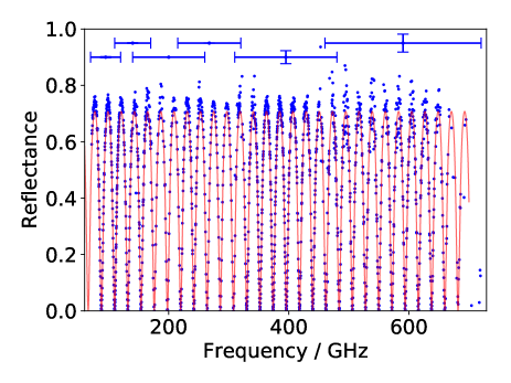
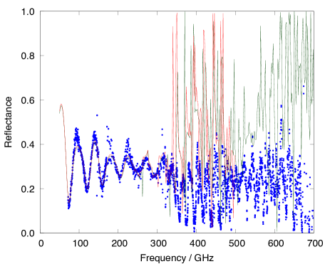
The high-resistivity silicon discs for F1, D, and L1 were part of the same order111Miyoshi Ltd. park15.wakwak.com/~miyoshi, Japan and arrived in the same shipment. We therefore assumed the same material properties for all three. Using reflectance measurements we fit for the index and loss tangent of F1 and found and loss tangent ; see Figure 1. Samples F2 and L2 were from a second order and shipment, 222University Wafer Inc. universitywafer.com, USA so we assumed the same material properties for both. We measured transmittance of F2, fit for index and loss, and found and loss tangent . Table 1 summarizes the information about the samples.
II.2 Laser ablation
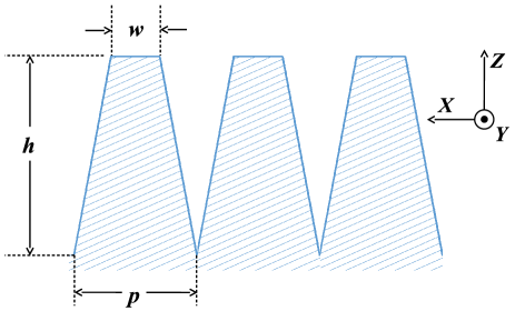
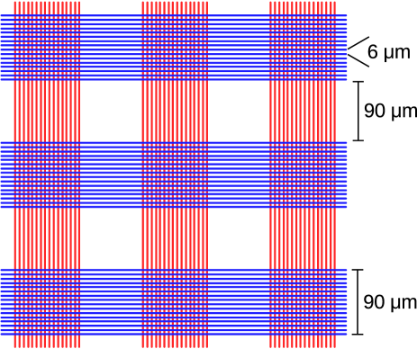
We machined L1 and L2 with parameters that were similar to our earlier laser ablation of SWS on alumina and sapphire;Matsumura et al. (2016b) the parameters of the geometry and the coordinate system are shown in Figure 2. The laser operated at a wavelength of 515 nm with a repetition rate of 400 kHz, 7 ps pulse width, and an average power of 28.5 W for L1 and 27 W for L2. The beam was focused at the surface of the silicon disc and had a width of 8 m. The laser was scanned across the entire sample at 2.5 m/sec in a raster pattern as shown in Figure 3. This pattern created a series of orthogonal grooves and pyramids with a designed pitch of 180 m. The scan was repeated 80 times. The total machining time for L1 was 3.4 hours for a 5 cm diameter disc. For L2 the grid patterns on the two sides were oriented at 45° with respect to each other. The total machining time for both sides was 6.8 hours. We did not attempt to optimize the ablation rate.
II.3 Dicing saw
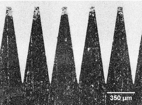
Sample D was machined using a custom made beveled dicing saw. The blade had a maximum thickness of 300 m. Imaging the profile of the first cut, we measured that the blade tip was m wide and the bevel angle was 81.6° providing a usable cutting depth of 1.04 mm. We produced pyramids by cutting 108 parallel grooves symmetrically placed about a diameter with a feed rate of 1 mm/sec, rotating the sample by , and cutting 107 more grooves with a feed rate of 0.8 mm/sec. The grooves had a designed pitch m and designed depth m to produce square pyramids with m. During machining, less than 1 % of the pyramids broke. The total machining time was 3 hours.
III Shape Measurements and Results
III.1 Measurements
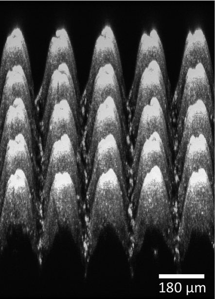
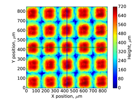
We used a Nikon A1RMP confocal microscope to image L1 and L2. The surfaces of D were too smooth to produce sufficient diffuse reflection, so we used a Keyence VHX-5000 optical microscope. Both microscopes had plane resolution of 2 m. We imaged 9 locations on L1 and 5 locations on each side of L2. At each location we took a series of images spaced in by 5 m and constructed a 3-dimensional image and a height map. Examples are shown in Figures 4 and 5, respectively.
Using the images, we measured the geometrical properties of the samples, including the height , pitch , and, where relevant, the width of the peak . The ablation caused deeper troughs at the intersection of grooves. We determined the height of the L1 and L2 pyramids by finding the median coordinate of the peaks and troughs, the red and blue regions seen in Figure 5. The measured height is quoted as the difference between these medians. Table 2 gives the mean height, pitch, and width, and the standard deviations of the values across all imaged areas.
| Sample | Heighta | Pitcha | Peak widtha |
| [m] | [m] | [m] | |
| D | |||
| L1 | N.A.b | ||
| L2(side A) | N.A.b | ||
| L2(side B) | N.A.b | ||
| aThe uncertainty quoted is the standard deviation | |||
| from multiple imaged areas. | |||
| bL1 and L2 did not have well-defined flat peaks. | |||
For D we found it more instructive to image a side view along the -axis and view the SWS in profile in the plane. This view is shown in Figure 6. For this sample, since the grooves were of uniform depth, the pyramid height was the same as the depth of the groove. We measured the depth of 17 grooves in the center of the sample by imaging the cut profiles. The mean and standard deviation are given in Table 2. To characterize blade wear we also imaged two grooves, one made 100 cuts after the other, a total of cut length 465 cm. The depth difference was 33 m.
III.2 Comments Regarding the Laser Ablated Shapes
The measured pitch of L1 and L2 matches the design value. It is a factor of 2.2 smaller than the pitch reported by Datta et al. (2013) who used sequential dicing with commercially available dicing saws. It is a factor of 1.8 smaller than the pitch of the SWS we recently laser-ablated on alumina and sapphire.Matsumura et al. (2016b)
The height of the L2 pyramids was 17 % smaller than the height of pyramids on L1, while the laser power was only 5 % lower. We suggest the following explanation. L2 was three times thicker than L1, implying that during ablation at similar incident power L1 was likely to be hotter than L2. Thorstensen and Foss (2012) reported a decrease in the ablation threshold of silicon with increasing temperature. Therefore the ablation threshold of L1 was lower than that of L2. In an earlier publication Schütz et al. (2016) we noted that ablation along a sloped face stops when the energy density of the beam dilutes below the ablation threshold. The effect is purely geometrical—a normally incident beam becomes elliptical when projected onto the ablated, sloped surface—and thus the maximum slope is calculable from a known ablation threshold. The higher the ablation threshold, the shallower the maximum slope. We hypothesize the combination of lower laser power and higher ablation threshold, due to the cooler substrate, produced a shallower slope angle on L2 of 84° vs 85° on L1. This is sufficient to explain the difference in heights.
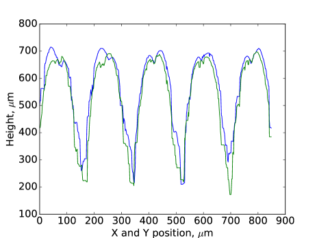
The ablation images show most of the pyramid tips are cracked. This may be a consequence of excessively high energy density. With this silicon ablation we are using J/m2/pulse. With sapphire, also a single crystal, we used an energy density per pulse that was 15 times lower and observed no cracking. The majority of the factor of 15 is due to the 3.75 times smaller spot diameter we used with silicon, a consequence of striving to reach smaller pitch and pyramid tips. The ablated shape repeatability is good as shown in Figure 7.
III.3 Comments Regarding the Diced Pyramid Shapes
The SWS on D were a regular array of truncated, square-based pyramids which matched the designed pitch of 350 m but were 25 m shorter than the 1000 m designed height. The height discrepancy was likely due to uncertainty in the absolute surface position of the wafer while being machined. However, the cut-to-cut repeatability in height was 3 m or better as shown by the small measured variation in height across 17 successive cuts.
We measured a 33 m decrease in structure height after 100 cuts, 465 cm of cut length. This difference was due to either blade wear or a slightly tilted sample mount. Assuming the entire height difference was due to blade wear, we calculated 0.07 m of wear per cm of cut length. If a large sample was machined, it would be important to re-zero the blade position or continuously adjust the depth to account for wear. Measurements on a different blade indicated negligible wear over 160 cuts, 720 cm of cut length. More data is needed before definitive information is available regarding beveled blade wear.
Sample D showed a negligible number of broken pyramids. We did not attempt to optimize the trade-off between structure robustness, blade feed-rate, and blade wear. Datta et al. (2013) used a factor of 50 higher feed-rate, suggesting the feed-rate with the beveled saw can be increased.
IV Optical Performance
IV.1 Measurement Procedure
We measured the reflectance of L1, L2, D, and F2 in two polarizations and six frequency bands between 70 and 720 GHz: 70–120 GHz, 110–170 GHz, 140–260 GHz, 215–320 GHz, 310–480 GHz, and 460–720 GHz. We measured F1 at the same frequencies, but in one polarization only. We measured transmittance of F2, L1, and L2 in four bands between 70 and 320 GHz: 70–120 GHz, 110–170 GHz, 140–260 GHz, and 215–320 GHz. The measurements were made at the Institute for Terahertz Science and Technology (ITST) at the University of California, Santa Barbara. The reflectance setup is described in Bailey et al. (2015) The transmittance setup was similar but the sample was placed just after the source, and a gold mirror replaced the reflectance sample. All measurements with samples were normalized using data runs without samples.
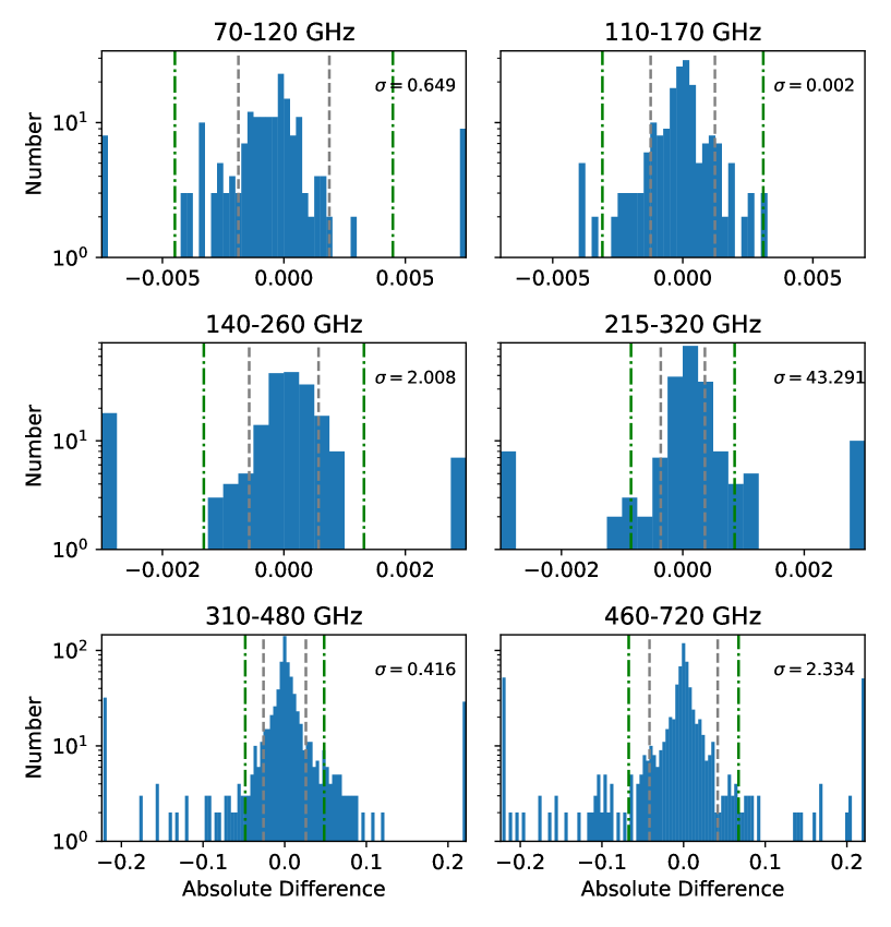
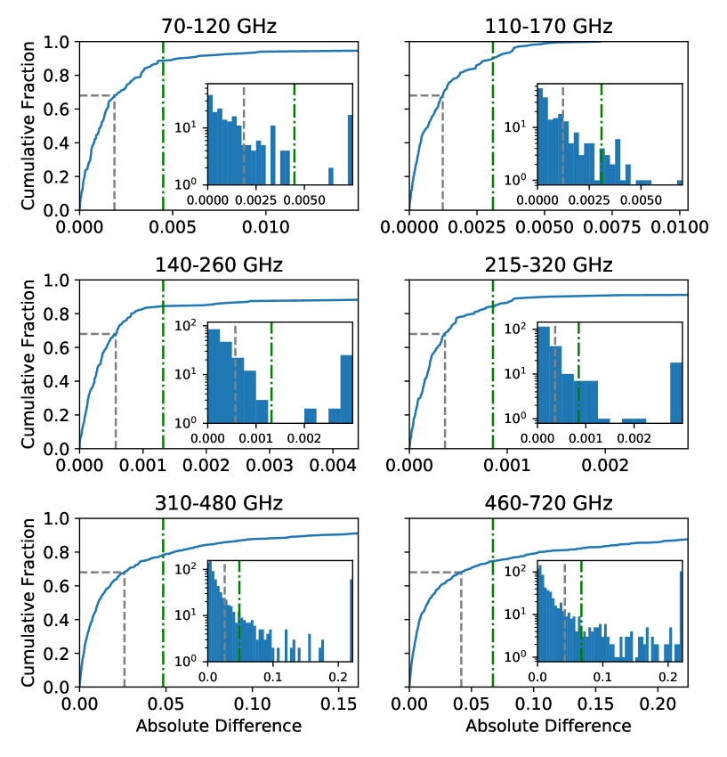
The ITST data were taken twice for each measurement without changing the setup. The difference between these measurements was used to remove outliers and estimate a measurement error per point. An example of one such difference, from the pair of measurements on F1, is shown in Figure 8. There are two primary sources of higher levels of noise: (1) lower source power output near band edges, and (2) an atmospheric water line at 557 GHz.van Exter, Fattinger, and Grischkowsky (1989) From the pair difference data we calculated the mean and the median absolute deviation (MAD) per band. The means were always within one MAD of zero. We removed as outliers all data with difference greater than MAD from the mean. We calculated the distribution and cumulative distribution for the pair difference data and assigned the measurement uncertainty per point as the level at which the cumulative distribution reached 68 %. These measurement uncertainties are shown for all data sets as single error bars per band. For clarity, they are displayed at an arbitrary vertical offset. The horizontal extent is the bandwidth over which the measurement error was calculated. A more detailed description of the data cuts and measurement uncertainty estimation is given in the Appendix.
IV.2 Measurements
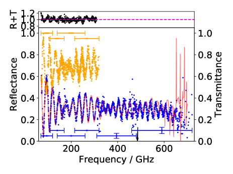
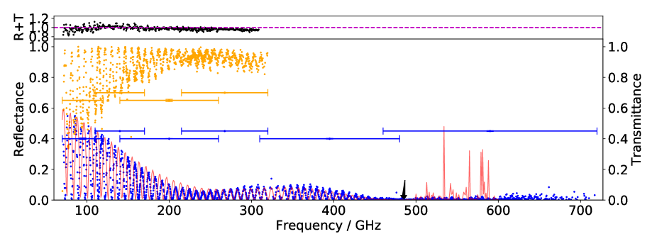
Figures 9, 10, and 11 show reflectance measurements of L1, L2, and D as well as the sum of transmittance and reflectance, where relevant. The Figures also give the upper frequency limit where diffraction becomes significant due to the pitch of the SWS. We discuss this diffraction in Section IV.3.
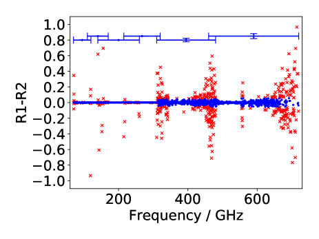
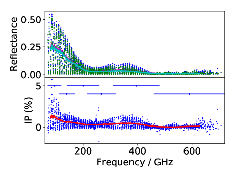
To characterize the polarization properties of the samples we calculated the difference in reflectance between measurements in two orthogonal polarizations. Figure 12 shows the reflectance data for L2. It also shows the level of instrumental polarization (IP) defined as
| (1) |
Instrumental polarization represents the level of conversion of unpolarized to polarized light by an instrument or one of its components. To calculate IP we used the reflectance data for each sample and assumed low loss; . For L1, L2, and D the maximum IP, averaged across 25 % fractional bandwidth, from 70–700 GHz was 1.2 %, 1.4 %, and 1.6 % respectively.
Measurements in two polarization states on F2, for which the IP should have been zero, gave band averaged () IP of less than below 320 GHz, less than from 320–490 GHz, and less than from 490–700 GHz. This indicated that below 490 GHz the measured IP due to the SWS was at or below the % level. Above 490 GHz we placed an upper limit of 1.5 % on the IP.
IV.3 Modeling
We modeled transmittance and reflectance using an electromagnetic finite element analysis code (HFSS)ANSYS (2016) and in some cases augmented it with calculations using rigorous coupled-wave analysis (RCWA).Moharam et al. (1995); Synopsys (2016)
We used the 3-dimensional image of L1 to construct a solid model of a single pyramid. This model pyramid was imported into the FEA and placed on a 1.287 mm thick substrate (the thickness of the native sample minus 0.720 mm, the height of L1). An infinite planar sample was simulated using periodic boundary conditions.
We reconstructed a single pyramid for each side of L2, placed them on each side of a 4.871 mm substrate, and simulated L2 in the same way as L1. To facilitate periodic boundary conditions we ignored the 45° rotation between the patterns on the two sides.
For D, we constructed a square based, truncated pyramid using , , and as measured and reported in Table 2. The pyramid was placed on a 1.037 mm thick substrate and duplicated using periodic boundary conditions.
The results of the FEA simulations are shown in Figures 9, 10, and 11. There was generally good agreement between simulations and data at frequencies up to and somewhat above the ‘diffraction frequency’ , which is marked with a black arrow. For L2 the data have a fringe pattern that has 4 % lower frequency than the simulation. We comment on this in Section IV.4. The frequency was the lowest frequency at which we expected diffraction and constructive interference inside the substrate to be significant. The constructive interference was due to the periodic structure of the pyramids and occurred at frequencies above
| (2) |
where and are integers. At frequencies above the FEA showed strong reflections, but the data do not.
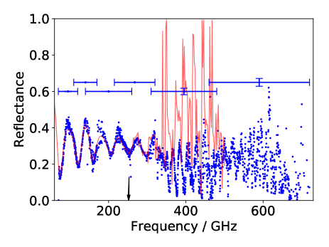
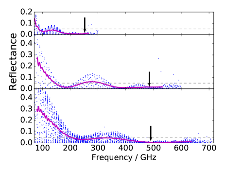
We cross-checked the results of the FEA using RCWA. Figure 13 shows the measured reflectance of D and the simulated reflectance using RCWA and FEA. All three were consistent below GHz. Above 252 GHz, at which the effect of diffraction was expected to appear with modes , RCWA and HFSS agree qualitatively; both showed high reflectance at similar frequencies, but the exact levels were different. We propose the following explanation for the discrepancy between simulations and data. The simulations duplicated one pyramid to create exactly periodic, infinite structures. Exactly periodic, infinite structures lead to high resonances which produce sharp spikes in reflection. However, the real sample was finite and consisted of pyramids which were all different in shape. A detailed comparison between the FEA, RCWA, and the data in the diffraction regime is beyond the scope of this paper, but it is interesting to note that measured data did not show the strong diffraction features suggested by simple calculations, indicating that the usable bandwidth of SWS-ARC may not be limited by .
IV.4 Comments Regarding Optical Performance
Since FEA simulations agreed with measurements below , we assessed performance of L1 and D up to by simulating silicon substrates coated on both sides with SWS matching those measured for L1 and D. These simulations are shown in Figure 14 along with the measured reflectance of L2. The Figure also shows reflectance averaged over 25 % fractional bandwidth, as would be appropriate for typical CMB experiments using bolometers.
Beveled dicing saws are an efficient way to remove material and are thus suitable for fabricating relatively deep, large pitch structures. Therefore, beveled saws are particularly suitable for applications at lower frequencies. Averaged over fractional bandwidth, reflectance drops below 5 % at 87 GHz. Doubling of the height of the pyramid would halve this frequency to approximately 44 GHz. Laser ablation is more efficient when patterning smaller structures. When averaged with 25 % fractional bandwidth, reflectance on the simulated two-sided L1 drops below 5 % at 144 GHz. The bandwidth with less than 5 % reflectance extends up to GHz, and higher if turns out to not limit the performance of the SWS. That these are realistic predictions is demonstrated by measurements of L2 (Figure 14). Defining the high frequency edge of an ‘effective band’ as and the low frequency edge as , we list the effective bands for L1, L2, and D, in Table 3. The frequency is that frequency at which the 25 % fractional bandwidth averaged reflectance drops below 5 %. The Table also gives the average reflectance within the effective band.
| Sample | Effective band | Average reflectancea |
|---|---|---|
| [GHz] | [%] | |
| L1b | 144–485 | 2.0 % |
| L2 | 202–490 | 2.9 % |
| Db | 87–252 | 2.8 % |
| a Averaged over the Effective band. | ||
| b From two sided FEA simulation using measured | ||
| SWS shape. | ||
We attribute the difference in fringe frequency between the simulation of L2 and data (Figure 10) to a crude approximation of the sample. As discussed in Section IV.3, the simulation is based on duplicating only one pyramid for each side of the surface, thus ignoring variations in shape, pyramid height, and thickness of the remaining material.
All three data sets, the simulated two-sided D and L1, and the measured L2, suggest a straight pyramid is not the optimal shape. There is a lobe of increased reflectance at frequencies above the onset of low-reflectance. Impedance matching theory suggests the implementation of a Klopfenstein profile Grann, Moharam, and Pommet (1995) to reduce this lobe.
V Summary
We presented two novel approaches to producing ARC on silicon for the MSM: laser ablation and dicing with beveled saws. The optical performance is summarized in Table 3. The SWS, laser ablated on both sides of a silicon disc, reduced 25 % band averaged reflectance to below 5 % over a fractional bandwidth of 83 % centered on 346 GHz. The dicing saw structures were larger, in both pitch and height, making them effective at lower frequencies. The dicing saw structures reduced reflectance to below 5 % over a fractional bandwidth of 97 % centered on 170 GHz. These effective bandwidths are sufficient for most currently deployed cosmic microwave background instruments, but would need to be increased to 150 % fractional bandwidth to meet the needs of all upcoming instruments. The effective band of both methods was limited by the structure height at low frequencies and pitch at high frequencies.
Machining times for both methods were similar. It took 3.4 hours to ablate one side of a 20 cm2 disc and 3 hours to machine 16 cm2 with dicing saws. Machining time for both methods can be improved by optimizing the machining parameters. To our knowledge, this is the first SWS-ARC for the MSM produced using these techniques.
Acknowledgements.
We thank two anonymous referees for detailed and helpful comments. The authors acknowledge use of resources provided by the University of Minnesota Imaging Center (http://uic.umn.edu) and Minnesota Supercomputing Institute (http://www.msi.umn.edu). The research described in this paper used facilities of the Midwest Nano Infrastructure Corridor (MINIC), a part of the National Nanotechnology Coordinated Infrastructure (NNCI) program of the National Science Foundation. The transmittance and reflectance measurements were performed at the ITST Terahertz Facilities at UCSB, which have been upgraded under NSF Award No. DMR-1126894. This work was partially supported by JSPS KAKENHI Grant Number 15H05441; the Mitsubishi foundation (grant number 24, JFY2015, in science and technology); the World Premier International Research Center Initiative (WPI), MEXT, Japan; and the JSPS Core-to-Core Program, Advanced Research Networks.- ARC
- anti-reflection coatings
- CMB
- cosmic microwave background
- MSM
- millimeter and sub-millimeter
- SWS
- sub-wavelength structures
- FEA
- finite element analysis
*
Appendix A Data Cuts and Error Estimation
To remove outliers and estimate uncertainty per point we used the difference between two subsequent data runs on the same sample with the setup unchanged. The difference vs frequency for F1 is shown in Figure 8 and we use these data as an example. The same procedure was used with pair differences for all measurements.
Pair difference distributions and cumulative distributions for each of the 6 measurement bands are shown in Figures 15 and 16, respectively. The data are not Gaussian-distributed and therefore the standard deviation is a poor estimator for the variance for the majority of the data. We used the median absolute deviation (MAD) instead. For a Gaussian distribution , however this ratio ranged between 2.5 and for the 6 pair difference measurements of F1. The calculated standard deviations for each of the 6 bands are shown in Figure 15.
We removed all points that were more than 4.5 MAD from the mean of the difference data. This cut removed the majority of the long outlier tail; see Figure 16. We chose this criterion because for a Gaussian distribution MAD, and because it was reasonable based on the cumulative distributions. We estimated measurement errors for each measurement and for each band by finding the difference value in the cumulative distribution of absolute values that included 68 % of the raw data, that is, prior to outlier removal. This is shown by the grey dashed lines in Figure 16. We used the cumulative distribution of absolute values because the distribution of did not depend on which data set was labeled or . These measurement errors are plotted at an arbitrary vertical offset in Figures 1, 8, 9, 10, 11, and 12. The horizontal extent shows the width of each of the frequency bands.
We tested the sensitivity of our calculated values to various data cuts. The values which could be affected are average reflectance on L2, and the maximum IP for D, L1, and L2. Using the cumulative distributions, we removed data in each band with the largest pair difference values using thresholds which kept 70 %, 80 %, 90 %, or 95 % of the data. Across these removal criteria we found average reflectance on L2 changed by 0.1 percentage points. Maximum IP changed by less than 0.3 percentage points for D and L1 and by 0.8 for L2.
References
- Lamb (1996) J. W. Lamb, Int. J. IR and Millimeter Waves 17, 1997 (1996).
- Thornton et al. (2016) R. J. Thornton, P. A. R. Ade, S. Aiola, F. E. Angilè, M. Amiri, J. A. Beall, D. T. Becker, H.-M. Cho, S. K. Choi, P. Corlies, K. P. Coughlin, R. Datta, M. J. Devlin, S. R. Dicker, R. Dünner, J. W. Fowler, A. E. Fox, P. A. Gallardo, J. Gao, E. Grace, M. Halpern, M. Hasselfield, S. W. Henderson, G. C. Hilton, A. D. Hincks, S. P. Ho, J. Hubmayr, K. D. Irwin, J. Klein, B. Koopman, D. Li, T. Louis, M. Lungu, L. Maurin, J. McMahon, C. D. Munson, S. Naess, F. Nati, L. Newburgh, J. Nibarger, M. D. Niemack, P. Niraula, M. R. Nolta, L. A. Page, C. G. Pappas, A. Schillaci, B. L. Schmitt, N. Sehgal, J. L. Sievers, S. M. Simon, S. T. Staggs, C. Tucker, M. Uehara, J. van Lanen, J. T. Ward, and E. J. Wollack, Ap. J. Suppl. 227, 21 (2016).
- Eimer et al. (2010) J. R. Eimer, P. A. R. Ade, D. J. Benford, C. L. Bennett, D. T. Chuss, D. J. Fixsen, A. J. Kogut, P. Mirel, C. E. Tucker, G. M. Voellmer, and E. J. Wollack, in Ground-based and Airborne Telescopes III, Proceedings of the SPIE, Vol. 7733 (2010) p. 77333B.
- Mitsui et al. (2015) K. Mitsui, T. Nitta, N. Okada, Y. Sekimoto, K. Karatsu, S. Sekiguchi, M. Sekine, and T. Noguchi, Journal of Astronomical Telescopes, Instruments, and Systems 1, 025001 (2015).
- Edwards et al. (2012) J. M. Edwards, R. O’Brient, A. T. Lee, and G. M. Rebeiz, IEEE Transactions on Antennas and Propagation 60, 4082 (2012).
- Sekiguchi et al. (2015) S. Sekiguchi, T. Nitta, K. Karatsu, Y. Sekimoto, N. Okada, T. Tsuzuki, S. Kashima, M. Sekine, T. Okada, S. Shu, M. Naruse, A. Dominjon, and T. Noguchi, IEEE Transactions on Terahertz Science and Technology 5, 49 (2015).
- Onaka et al. (2007) T. Onaka, H. Matsuhara, T. Wada, N. Fujishiro, H. Fujiwara, M. Ishigaki, D. Ishihara, Y. Ita, H. Kataza, W. Kim, T. Matsumoto, H. Murakami, Y. Ohyama, S. Oyabu, I. Sakon, T. Tanabé, T. Takagi, K. Uemizu, M. Ueno, F. Usui, H. Watarai, M. Cohen, K. Enya, T. Ootsubo, C. P. Pearson, N. Takeyama, T. Yamamuro, and Y. Ikeda, PASJ 59, S401 (2007).
- Deen et al. (2008) C. P. Deen, L. Keller, K. A. Ennico, D. T. Jaffe, J. P. Marsh, J. D. Adams, N. Chitrakar, T. P. Greene, D. J. Mar, and T. Herter, in Ground-based and Airborne Instrumentation for Astronomy II, Proceedings of the SPIE, Vol. 7014 (2008) p. 70142C.
- Gully-Santiago et al. (2010) M. Gully-Santiago, W. Wang, C. Deen, D. Kelly, T. P. Greene, J. Bacon, and D. T. Jaffe, in Modern Technologies in Space- and Ground-based Telescopes and Instrumentation, Proceedings of the SPIE, Vol. 7739 (2010) p. 77393S.
- Lau et al. (2006) J. Lau, J. Fowler, T. Marriage, L. Page, J. Leong, E. Wishnow, R. Henry, E. Wollack, M. Halpern, D. Marsden, and G. Marsden, Appl. Opt. 45, 3746 (2006), astro-ph/0701091 .
- Gatesman et al. (2000) A. J. Gatesman, J. Waldman, M. Ji, C. Musante, and S. Yagvesson, IEEE Microwave and Guided Wave Letters 10, 264 (2000).
- Wheeler et al. (2014) J. D. Wheeler, B. Koopman, P. Gallardo, P. R. Maloney, S. Brugger, G. Cortes-Medellin, R. Datta, C. D. Dowell, J. Glenn, S. Golwala, C. McKenney, J. J. McMahon, C. D. Munson, M. Niemack, S. Parshley, and G. Stacey, in Millimeter, Submillimeter, and Far-Infrared Detectors and Instrumentation for Astronomy VII, Proceedings of the SPIE, Vol. 9153 (2014) p. 91532Z.
- Kamizuka et al. (2012) T. Kamizuka, T. Miyata, S. Sako, H. Imada, T. Nakamura, K. Asano, M. Uchiyama, K. Okada, T. Wada, T. Nakagawa, T. Onaka, and I. Sakon, in Modern Technologies in Space- and Ground-based Telescopes and Instrumentation II, Proceedings of the SPIE, Vol. 8450 (2012) p. 845051.
- Datta et al. (2013) R. Datta, C. D. Munson, M. D. Niemack, J. J. McMahon, J. Britton, E. J. Wollack, J. Beall, M. J. Devlin, J. Fowler, P. Gallardo, J. Hubmayr, K. Irwin, L. Newburgh, J. P. Nibarger, L. Page, M. A. Quijada, B. L. Schmitt, S. T. Staggs, R. Thornton, and L. Zhang, Appl. Opt. 52, 8747 (2013).
- Benson et al. (2014) B. A. Benson, P. A. R. Ade, Z. Ahmed, S. W. Allen, K. Arnold, J. E. Austermann, A. N. Bender, L. E. Bleem, J. E. Carlstrom, C. L. Chang, H. M. Cho, J. F. Cliche, T. M. Crawford, A. Cukierman, T. de Haan, M. A. Dobbs, D. Dutcher, W. Everett, A. Gilbert, N. W. Halverson, D. Hanson, N. L. Harrington, K. Hattori, J. W. Henning, G. C. Hilton, G. P. Holder, W. L. Holzapfel, K. D. Irwin, R. Keisler, L. Knox, D. Kubik, C. L. Kuo, A. T. Lee, E. M. Leitch, D. Li, M. McDonald, S. S. Meyer, J. Montgomery, M. Myers, T. Natoli, H. Nguyen, V. Novosad, S. Padin, Z. Pan, J. Pearson, C. Reichardt, J. E. Ruhl, B. R. Saliwanchik, G. Simard, G. Smecher, J. T. Sayre, E. Shirokoff, A. A. Stark, K. Story, A. Suzuki, K. L. Thompson, C. Tucker, K. Vanderlinde, J. D. Vieira, A. Vikhlinin, G. Wang, V. Yefremenko, and K. W. Yoon, in Society of Photo-Optical Instrumentation Engineers (SPIE) Conference Series, Society of Photo-Optical Instrumentation Engineers (SPIE) Conference Series, Vol. 9153 (2014) p. 1.
- Posada et al. (2016) C. M. Posada, P. A. R. Ade, A. J. Anderson, J. Avva, Z. Ahmed, K. S. Arnold, J. Austermann, A. N. Bender, B. A. Benson, L. Bleem, K. Byrum, J. E. Carlstrom, F. W. Carter, C. Chang, H.-M. Cho, A. Cukierman, D. A. Czaplewski, J. Ding, R. N. S. Divan, T. de Haan, M. Dobbs, D. Dutcher, W. Everett, R. N. Gannon, R. J. Guyser, N. W. Halverson, N. L. Harrington, K. Hattori, J. W. Henning, G. C. Hilton, W. L. Holzapfel, N. Huang, K. D. Irwin, O. Jeong, T. Khaire, M. Korman, D. L. Kubik, C.-L. Kuo, A. T. Lee, E. M. Leitch, S. Lendinez Escudero, S. S. Meyer, C. S. Miller, J. Montgomery, A. Nadolski, T. J. Natoli, H. Nguyen, V. Novosad, S. Padin, Z. Pan, J. E. Pearson, A. Rahlin, C. L. Reichardt, J. E. Ruhl, B. Saliwanchik, I. Shirley, J. T. Sayre, J. A. Shariff, E. D. Shirokoff, L. Stan, A. A. Stark, J. Sobrin, K. Story, A. Suzuki, Q. Y. Tang, R. B. Thakur, K. L. Thompson, C. E. Tucker, K. Vanderlinde, J. D. Vieira, G. Wang, N. Whitehorn, V. Yefremenko, and K. W. Yoon, in Millimeter, Submillimeter, and Far-Infrared Detectors and Instrumentation for Astronomy VIII, Vol. 9914 (2016) pp. 991417–991417–11.
- Inoue et al. (2016) Y. Inoue, P. Ade, Y. Akiba, C. Aleman, K. Arnold, C. Baccigalupi, B. Barch, D. Barron, A. Bender, D. Boettger, J. Borrill, S. Chapman, Y. Chinone, A. Cukierman, T. de Haan, M. A. Dobbs, A. Ducout, R. Dünner, T. Elleflot, J. Errard, G. Fabbian, S. Feeney, C. Feng, G. Fuller, A. J. Gilbert, N. Goeckner-Wald, J. Groh, G. Hall, N. Halverson, T. Hamada, M. Hasegawa, K. Hattori, M. Hazumi, C. Hill, W. L. Holzapfel, Y. Hori, L. Howe, F. Irie, G. Jaehnig, A. Jaffe, O. Jeong, N. Katayama, J. P. Kaufman, K. Kazemzadeh, B. G. Keating, Z. Kermish, R. Keskitalo, T. S. Kisner, A. Kusaka, M. Le Jeune, A. T. Lee, D. Leon, E. V. Linder, L. Lowry, F. Matsuda, T. Matsumura, N. Miller, K. Mizukami, J. Montgomery, M. Navaroli, H. Nishino, H. Paar, J. Peloton, D. Poletti, G. Puglisi, C. R. Raum, G. M. Rebeiz, C. L. Reichardt, P. L. Richards, C. Ross, K. M. Rotermund, Y. Segawa, B. D. Sherwin, I. Shirley, P. Siritanasak, N. Stebor, R. Stompor, J. Suzuki, A. Suzuki, O. Tajima, S. Takada, S. Takatori, G. P. Teply, A. Tikhomirov, T. Tomaru, N. Whitehorn, A. Zahn, and O. Zahn, in Millimeter, Submillimeter, and Far-Infrared Detectors and Instrumentation for Astronomy VIII, Proceedings of the SPIE, Vol. 9914 (2016) p. 99141I.
- Matsumura et al. (2016a) T. Matsumura, Y. Akiba, K. Arnold, J. Borrill, R. Chendra, Y. Chinone, A. Cukierman, T. de Haan, M. Dobbs, A. Dominjon, T. Elleflot, J. Errard, T. Fujino, H. Fuke, N. Goeckner-wald, N. Halverson, P. Harvey, M. Hasegawa, K. Hattori, M. Hattori, M. Hazumi, C. Hill, G. Hilton, W. Holzapfel, Y. Hori, J. Hubmayr, K. Ichiki, J. Inatani, M. Inoue, Y. Inoue, F. Irie, K. Irwin, H. Ishino, H. Ishitsuka, O. Jeong, K. Karatsu, S. Kashima, N. Katayama, I. Kawano, B. Keating, A. Kibayashi, Y. Kibe, Y. Kida, K. Kimura, N. Kimura, K. Kohri, E. Komatsu, C. L. Kuo, S. Kuromiya, A. Kusaka, A. Lee, E. Linder, H. Matsuhara, S. Matsuoka, S. Matsuura, S. Mima, K. Mitsuda, K. Mizukami, H. Morii, T. Morishima, M. Nagai, T. Nagasaki, R. Nagata, M. Nakajima, S. Nakamura, T. Namikawa, M. Naruse, K. Natsume, T. Nishibori, K. Nishijo, H. Nishino, T. Nitta, A. Noda, T. Noguchi, H. Ogawa, S. Oguri, I. S. Ohta, C. Otani, N. Okada, A. Okamoto, A. Okamoto, T. Okamura, G. Rebeiz, P. Richards, S. Sakai, N. Sato, Y. Sato, Y. Segawa, S. Sekiguchi, Y. Sekimoto, M. Sekine, U. Seljak, B. Sherwin, K. Shinozaki, S. Shu, R. Stompor, H. Sugai, H. Sugita, T. Suzuki, A. Suzuki, O. Tajima, S. Takada, S. Takakura, K. Takano, Y. Takei, T. Tomaru, N. Tomita, P. Turin, S. Utsunomiya, Y. Uzawa, T. Wada, H. Watanabe, B. Westbrook, N. Whitehorn, Y. Yamada, N. Yamasaki, T. Yamashita, M. Yoshida, T. Yoshida, and Y. Yotsumoto, Journal of Low Temperature Physics 184, 824 (2016a).
- Schütz et al. (2016) V. Schütz, K. Young, T. Matsumura, S. Hanany, J. Koch, O. Suttmann, L. Overmeyer, and Q. Wen, Journal of Laser Micro Nanoengineering 11, 204 (2016).
- Matsumura et al. (2016b) T. Matsumura, K. Young, Q. Wen, S. Hanany, H. Ishino, Y. Inoue, M. Hazumi, J. Koch, O. Suttman, and V. Schütz, Appl. Opt. 55, 3502 (2016b).
- Phillips et al. (2015) K. C. Phillips, H. H. Gandhi, E. Mazur, and S. K. Sundaram, Adv. Opt. Photon. 7, 684 (2015).
- Domke et al. (2016) M. Domke, G. Piredda, J. Zehetner, and S. Stroj, Journal of Laser Micro Nanoengineering 11, 100 (2016).
- Bonse et al. (2002) J. Bonse, S. Baudach, J. Krüger, W. Kautek, and M. Lenzner, Applied Physics A 74, 19 (2002).
- Schütz, Stute, and Horn (2013) V. Schütz, U. Stute, and A. Horn, Physics Procedia 41, 640 (2013).
- Her et al. (1998) T.-H. Her, R. J. Finlay, C. Wu, S. Deliwala, and E. Mazur, Applied Physics Letters 73, 1673 (1998).
- Ming et al. (2003) Z. Ming, Y. Gang, Z. Jing-Tao, and Z. Li, Chinese Physics Letters 20, 1789 (2003).
- Younkin et al. (2003) R. Younkin, J. E. Carey, E. Mazur, J. A. Levinson, and C. M. Friend, Journal of Applied Physics 93, 2626 (2003).
- Sheehy et al. (2005) M. A. Sheehy, L. Winston, J. E. Carey, C. M. Friend, and E. Mazur, Chemistry of Materials 17, 3582 (2005).
- Note (1) Miyoshi Ltd. park15.wakwak.com/~miyoshi, Japan.
- Note (2) University Wafer Inc. universitywafer.com, USA.
- Thorstensen and Foss (2012) J. Thorstensen and S. E. Foss, Journal of Applied Physics 112, 103514 (2012).
- Bailey et al. (2015) M. L. P. Bailey, A. T. Pierce, A. J. Simon, D. T. Edwards, G. J. Ramian, N. I. Agladze, and M. S. Sherwin, IEEE Transactions on Terahertz Science and Technology 5, 961 (2015).
- van Exter, Fattinger, and Grischkowsky (1989) M. van Exter, C. Fattinger, and D. Grischkowsky, Opt. Lett. 14, 1128 (1989).
- ANSYS (2016) ANSYS, (2016), HFSS, 3D Full-wave Electromagnetic Field Simulation, Electromagnetcis Suite 16.1.
- Moharam et al. (1995) M. G. Moharam, T. K. Gaylord, E. B. Grann, and D. A. Pommet, J. Opt. Soc. Am. A 12, 1068 (1995).
- Synopsys (2016) Synopsys, (2016), RSoft DiffractMOD v2016.03.
- Grann, Moharam, and Pommet (1995) E. B. Grann, M. G. Moharam, and D. A. Pommet, Journal of the Optical Society of America A 12, 333 (1995).