Also at ]Laboratoire Kastler Brossel, Paris.
Polarimetric analysis of stress anisotropy in nanomechanical silicon nitride resonators
Abstract
We realise a circular gray-field polariscope to image stress-induced birefringence in thin (sub-micron thick) silicon nitride (SiN) membranes and strings. This enables quantitative mapping of the orientation of principal stresses and stress anisotropy, complementary to, and in agreement with, finite element modeling (FEM). Furthermore, using a sample with a well known stress anisotropy, we extract a new value for the photoelastic (Brewster) coefficient of silicon nitride, . We explore possible applications of the method to analyse and quality-control stressed membranes with phononic crystal patterns.
Silicon nitride membranes and strings under high tensile stress have excellent mechanical and optical properties Zwickl et al. (2008); Wilson et al. (2009), making them a widely used platform to study the behaviour of mechanical systems in the quantum regime Purdy et al. (2013); Purdy, Peterson, and Regal (2013); Zhou et al. (2013); Underwood et al. (2015); Wilson et al. (2015); Peterson et al. (2016); Nielsen et al. (2016); Noguchi et al. (2016). Recently, further enhancement of these properties through in-plane patterning has been explored. Examples include one-Stambaugh et al. (2015) and two-dimensionalChen et al. (2016); Norte, Moura, and Gröblacher (2016); Bernard et al. (2016) subwavelength optical grating and photonic crystal structures which can boost the reflectivity of SiN beyond . In the mechanical domain, “trampoline” resonators Kleckner et al. (2011) combine thin tethers with a light central pad to achieve low-mass, low-frequency resonators with high quality factors Norte, Moura, and Gröblacher (2016); Reinhardt et al. (2016); Weaver et al. (2016). Patterning with phononic bandgap structures Ghadimi, Wilson, and Kippenberg (2016); Barasheed, Müller, and Sankey (2015); Tsaturyan et al. (2016) can suppress radiation losses and, if combined with optimised dissipation dilution through “soft clamping”Tsaturyan et al. (2016), yield extreme quality factors and room-temperature -products beyond .
In all instances of patterning, the stress relaxes to a new equilibrium distribution according to the pattern boundary conditions. This changes dramatically the mechanical, and potentially, via photoelastic coupling, optical properties of the structure. In absence of a laboratory diagnostic instrument, it has so far been necessary to rely on FEM to simulate the stress redistribution. In addition, little is known about the photoelastic coupling in silicon nitride Børkje and Girvin (2012); Grutter, Davanco, and Srinivasan (2015). To address these deficiencies, we have realised a highly sensitive polarimetric setup which allows quantitative imaging of stress-induced birefringence.
Among the numerous possibilities to implement an imaging polarimeter (or polariscope)Ajovalasit, Petrucci, and Scafidi (2015), we have chosen to build a circular gray-field polariscope. Its basic idea is to illuminate the sample with circularly polarised light, and analyse the ellipticity of the transmitted beam’s polarisation in a spatially resolved manner. This approach has a decisive advantage over plane polariscopes working with linear polarisation when it comes to measuring small optical retardation : as we will demonstrate, in the circular polariscope the optical signal is , whereas in the plane polariscope it is only . In our setup (Fig. 1 and Tab. 1), we use a light emitting diode (Thorlabs M780LP1) as a light source, followed by a bandpass filter that eases the requirements on achromaticity of the subsequent optical elements. The source is imaged on a diffuser which, together with an aspheric condenser lens, provides a Köhler-like illumination of the sample. Before reaching the sample, the circular polarisation state is defined by a high-contrast polariser and a quarter-wave plate(). After the sample, a motor-controlled rotating half-waveplate and a polarising beam splitter cube analyse the polarisation state. Rotating the waveplate was found to yield better results than rotating various kinds of polarisers, which tended to displace the beam and thus create image artifacts. A microscope objective (Achrovid 5x) and a plano-convex lens image part of the sample on a CCD camera (Mightex CGE B013-U) with a magnification of .

| LED central wavelength (nm) | 780 |
| Bandpass filter bandwidth (nm) | 10 |
| Working distance of the microscope objective (mm) | 37 |
| Focal length of the imaging lens (mm) | 400 |
| Pixel size (m) | 3.753.75 |
| Resolution of the CCD camera | 1280960 |
| Bit depth of the CCD camera ADC | 12 |
It is straightforward to compute the expected signal via Jones calculus. Each area element of the sample can be treated as a general retarder described by the Jones matrix
| (1) |
where is the azimuthal angle of the polarisation eigenstate basis with respect to a fixed laboratory reference, is the retardation phase, and
| (2) |
is the canonical rotation matrix. Specifically, in the case of stress birefringence of a SiN membrane, denotes the direction of the principal stress in the membrane plane, and is the retardation induced by stress anisotropy,
| (3) |
where is the wavelength of the light source, the stress anisotropy, the thickness of the sample and the Brewster coefficient, which is a material constant. The other waveplates can easily be represented by similar matrices, setting for quarter waveplates, and for half waveplates. The analyzer at the end projects the polarisation state, as described by the matrix
| (4) |
If we introduce as the angle of the output half waveplate with respect to the output polariser, the intensity at each camera pixel is given by , with
| (5) |
assuming, for simplicity, a perfect input polarisation .
We denote with the Fourier transform of the output signal with respect to time , during which the half-wave plate rotates with constant angular velocity . Then it is easy to show that
| (6) |
We can thus extract the entities of interest by calculating
| (7) |
and
| (8) |
Here, is an offset angle, given by the angle of the first polariser plus , which corresponds to the position of the quarter waveplate. Indeed, there is no phase shift when the axis of the quarter waveplate is aligned with the principal axis of the sample.
The data are acquired and processed as follows: images are taken at 10 angular positions for one full rotation. At each position we acquire a large number of frames (typically 150), from which a frame acquired with the shutter closed is subtracted. This is done in order to remove the dark current, which corresponds to an offset due to the thermal electrons detected by the CCD camera. The procedure is repeated without the sample to acquire background images. For each image, treated as a two-dimensional matrix, we calculate the normalized quantity . Finally, the background is subtracted from the measurements involving the sample. This yields a complex matrix, which is translated into the orientation and retardation following eqs. (7) and (8).
For initial validation, we performed a measurement on a sample with a particularly simple geometry, namely a nm thick silicon nitride ribbon. We used standard nanofabrication techniques to realise this sample, starting with low-pressure chemical vapor deposition (LPCVD) of nm stoichiometric silicon nitride on a m double-side polished silicon wafer. The chosen deposition parameters create a film with an isotropic tensile stress of ca. . Subsequently, ribbons are defined by UV photolithography and reactive ion etching. The photoresist is removed and the wafer is stripped of its native silicon oxide layer by a buffered hydrofluoric acid (BHF) dip. Finally, the ribbons are released using an anisotropic KOH etch from the wafer’s backside. Since the ribbons are clamped only from two sides, the stress in the free direction relaxes close to zero.
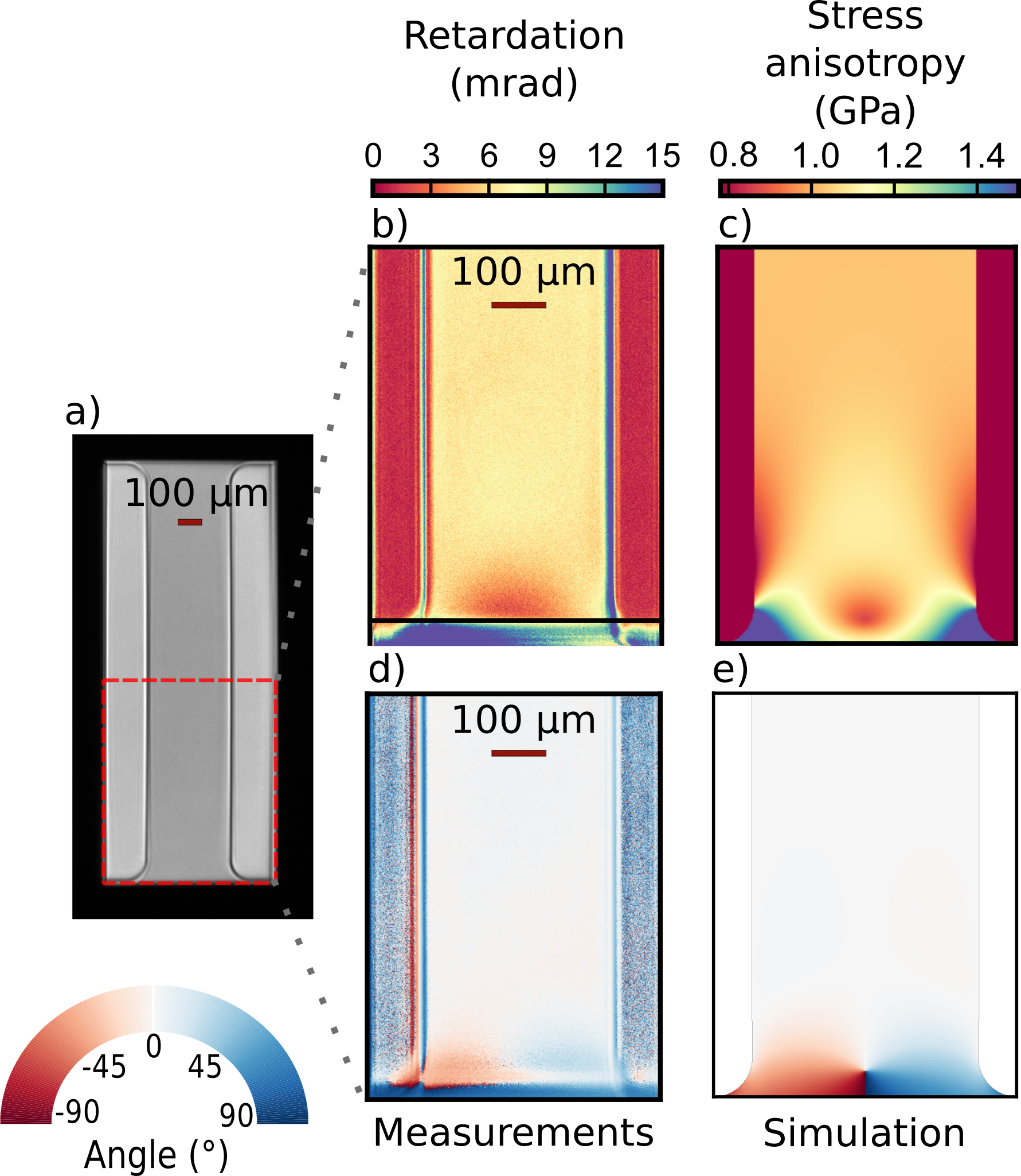
Figure 2 shows the measured stress birefringence of such ribbons as obtained using our method. The results agree well with our physical intuition, as well as finite-element modelling (COMSOL Multiphysics): at the center of the ribbon the stress is large along the direction of the ribbon and nonexistent in the orthogonal direction, so the anisotropy is maximal. Closer to the clamping region the ribbon also gets stressed in the orthogonal direction, due to the proximity to the silicon support, reducing the anisotropy. The higher stress anisotropy in the ribbon’s fillets could not be recovered in our setup, possibly due to diffraction artifacts (see below). The stress direction is also reproduced correctly: homogeneously along the ribbon in its center, while close to the clamp it rotates by , preserving the symmetry of the structure.

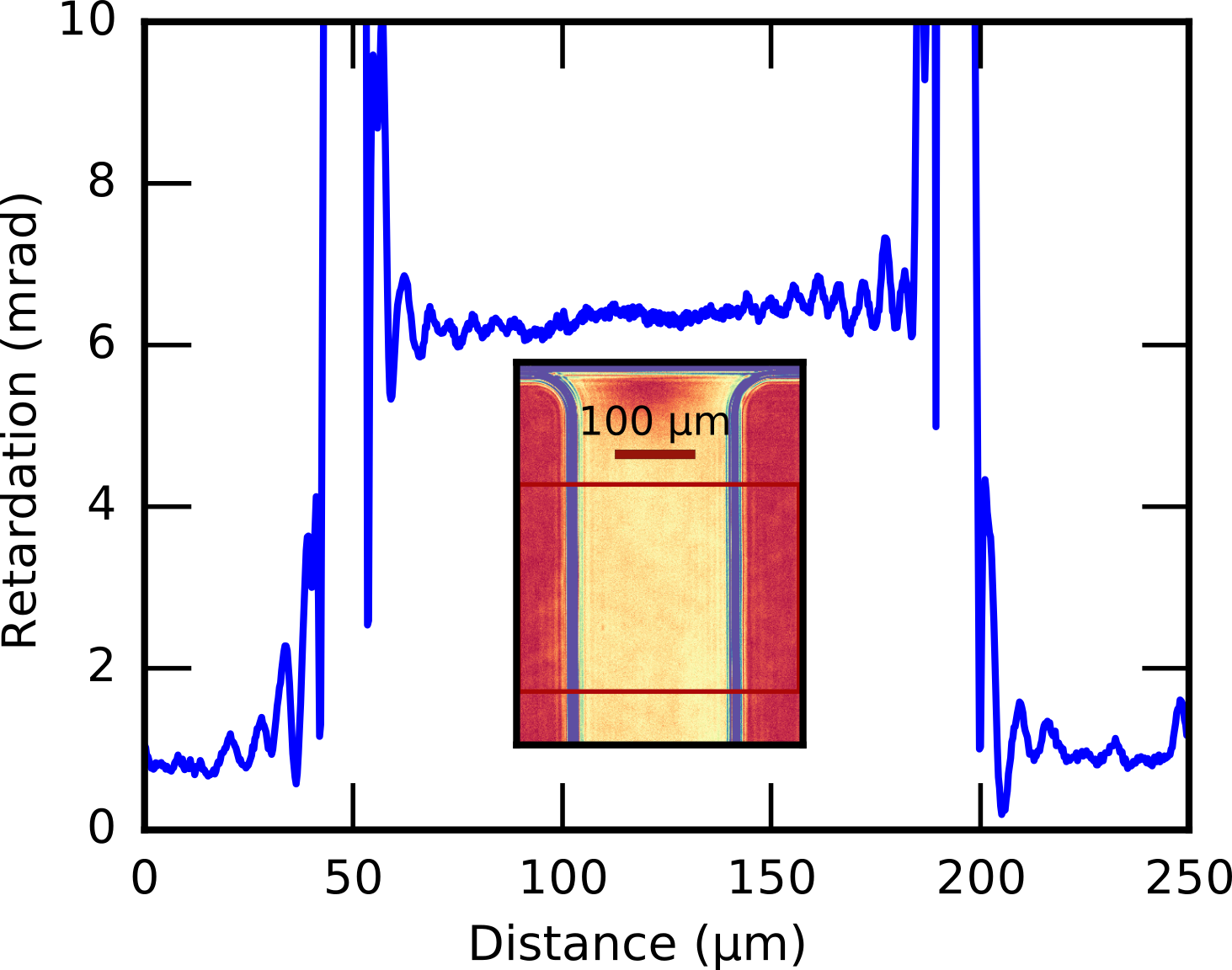
The good agreement prompts us to apply this approach to measure the Brewster coefficient, relating stress anisotropy with birefringence, of SiN, for which quantitative data is scarce Børkje and Girvin (2012); Grutter, Davanco, and Srinivasan (2015). To that end we measured a second ribbon, whose initial stress was carefully determined to be MPa before releasing of the ribbon111This measurement was conducted on a separate sample with a -nm thick SiN layer grown in the same conditions as the ribbon.. In order to take into account the change of the boundary conditions during the release of the ribbon, we have to correct this value by a factor , where is the Poisson ratio of the material, assumed here to be equal to . The result is presented in Figure 3. We obtain a retardation of by averaging a -area in the central region of the ribbon. For a quantitative comparison, we correct this value for the multiple reflections inside the film, which are not entirely negligible due to the relatively high () refractive index of SiN. To do so, we used a transfer matrix model for the complex transmittance of this sample222the transmittance of a membrane of thickness and refractive index is given by , expanding it to first order in a small variation of refractive index. This yielded a correction parameter of for the effective thickness of the sample. The Brewster coefficient of SiN can then be evaluated as
| (9) |
where nm is the sample thickness. Remarkably, this is two orders of magnitude lower than the value proposed by Campillo et al. Campillo and Hsu (2002), but close to the value of silica () Priestley (2001), another amorphous transparent dielectric. This mistake arises from the fact that this previous work measured the refractive index and the stress for different gas flow ratios during the LPCVD process, and not the variation of the refractive index due to mechanical stress.

With such calibration at hand, we proceed to applying polarimetric stress analysis to more complicated resonator structures. Membrane resonators with phononic bandgap shield are of particular interest. In the context of silicon nitride membranes it has been shown that phononic crystal structures can suppress transmission of vibrations Tsaturyan et al. (2014); Yu et al. (2014), resulting in suppression of dissipation through phonon tunneling Yu et al. (2014); Wilson-Rae (2008), whose avoidance had previously required delicate and often unreliable clamping techniquesWilson et al. (2009). Patterning a phononic crystal structure directly onto the membrane not only suppresses phonon tunneling losses, but also enhances the dilution of internal losses dramatically, enabling an increase in the quality factor by more than an order of magnitude Tsaturyan et al. (2016), as compared to conventional membrane resonators embedded in silicon phononic crystal structures. Stress analysis using polarimetry in such complex geometries can be a reliable and simple tool to assess the periodicity of stress anisotropy as required for the formation of a bandgap.
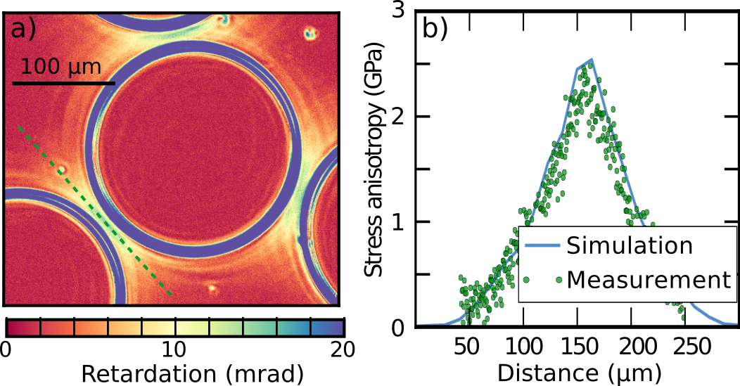
To demonstrate this potential, we realised membranes () with a honeycomb pattern of -diameter holes, fabricated using the same techniques as for the ribbons. Such a patterned membrane exhibits a bandgap as previously describedTsaturyan et al. (2016). Once again, we performed a measurement of the retardation, as described above, with the result shown in Figure 4. As expected, we observe an enhanced stress anisotropy in the tethers (i.e. the narrow regions between the circular holes), see Fig. 4a. In particular, a cut along a tether reveals a peak, symmetric with respect to the center of the tether, and a maximum stress anisotropy of . Excellent agreement with the predicted stress anisotropy in this region confirms the previously computed value of the Brewster coefficient.
Near the edges of the membrane, large retardation values () appears as dark blue rings around the holes (see Fig 4a). We attribute these to diffraction-related imaging artifacts. This is supported by the presence of several weak concentric rings around the holes, likely due to higher diffraction orders. In addition, the observation of these features already in single-shot images rules out excentric rotation as their cause.

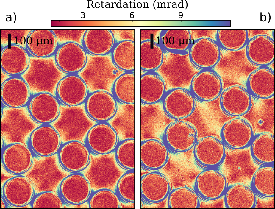
In spite of such artifacts, it is straightforward to recognise defective membranes. Figure 5 shows retardation images of an undamaged membrane and one with a broken tether, as a comparison. Defects in the perforated membrane structure cause a redistribution of the stress. One could envision using this approach in assessing the overall performance of the device (e.g. the quality factor), by comparing the stress profile of the defective device with simulations of an undamaged membrane resonator.

In conclusion, applied to -thick membrane resonators, our experimental setup achieves a resolution in retardation over a area. Using the measured Brewster coefficient, this corresponds to a resolution in stress anisotropy of . Thus we expect the method to deliver relevant results also for ultrathin () membranes of smaller dimensions. As an imaging modality, the present, very basic microscopy setup achieves moderate transverse resolution on the order of , impaired also by edge artifacts (likely diffraction-caused). It is nonetheless more than sufficient to assess the overall quality of patterned membrane resonators and localise defects. We have implemented a gray field polariscope optimised for extracting stress anisotropy in membrane resonators. We have validated the technique by comparing our measurement results with FEM simulations, and performed an independent measurement of the Brewster coefficient, correcting an older value found in the litteratureCampillo and Hsu (2002). In itself, this result is of interest for optomechanical systems relying on photoelastic coupling in silicon nitride Børkje and Girvin (2012); Grutter, Davanco, and Srinivasan (2015).
References
- Zwickl et al. (2008) B. M. Zwickl, W. E. Shanks, M. Jayich, C. Yang, C. Bleszynski Jayich, J. D. Thompson, and J. G. E. Harris, Applied Physics Letters 92, 103125 (2008).
- Wilson et al. (2009) D. J. Wilson, C. A. Regal, S. B. Papp, and H. J. Kimble, Physical Review Letters 103, 207204 (2009).
- Purdy et al. (2013) T. P. Purdy, P.-L. Yu, R. W. Peterson, N. S. Kampel, and C. A. Regal, Physical Review X 3, 031012 (2013).
- Purdy, Peterson, and Regal (2013) T. P. Purdy, R. W. Peterson, and C. Regal, 339, 1 (2013).
- Zhou et al. (2013) X. Zhou, F. Hocke, A. Schliesser, A. Marx, H. . Huebl, R. Gross, and T. J. Kippenberg, Nature Physics 9, 179 (2013).
- Underwood et al. (2015) M. Underwood, D. Mason, D. Lee, H. Xu, L. Jiang, A. B. Shkarin, K. Borkje, S. M. Girvin, and J. G. E. Harris, Physical Review A 92, 061801(R) (2015).
- Wilson et al. (2015) D. J. Wilson, V. Sudhir, N. Piro, R. Schilling, A. Ghadimi, and T. J. Kippenberg, Nature 524, 325 (2015).
- Peterson et al. (2016) R. Peterson, T. P. Purdy, N. Kampel, R. Andrews, P.-L. Yu, K. Lehnert, and C. Regal, Physical Review Letters 116, 063601 (2016), 1510.03911 .
- Nielsen et al. (2016) W. H. P. Nielsen, Y. Tsaturyan, C. B. Møller, E. S. Polzik, and A. Schliesser, PNAS 114, 62– (2016).
- Noguchi et al. (2016) A. Noguchi, R. Yamazaki, M. Ataka, H. Fujita, Y. Tabuchi, T. Ishikawa, K. Usami, and Y. Nakamura, New journal of Physics 18 (2016).
- Stambaugh et al. (2015) C. Stambaugh, H. Xu, U. Kemiktarak, J. Taylor, and J. Lawall, Annalen der Physik 527, 81 (2015), 1407.1709 .
- Chen et al. (2016) X. Chen, C. Chardin, K. Makles, C. Caër, S. Chua, R. Braive, I. Robert-Philip, T. Briant, P.-F. Cohadon, A. Heidmann, T. Jacqmin, and S. Deléglise, arXiv:1603.07200 (2016).
- Norte, Moura, and Gröblacher (2016) R. Norte, J. P. Moura, and S. Gröblacher, Physical Review Letters 116, 147202 (2016).
- Bernard et al. (2016) S. Bernard, C. Reinhardt, V. Dumont, Y.-A. Peter, and J. C. Sankey, Optics Letter 41, 5624 (2016).
- Kleckner et al. (2011) D. Kleckner, B. Pepper, E. Jeffrey, P. Sonin, S. M. Thon, and D. Bouwmeester, Optics Express 19, 19708 (2011).
- Reinhardt et al. (2016) C. Reinhardt, T. Müller, A. Bourassa, and J. C. Sankey, Physical Review X 6, 021001 (2016).
- Weaver et al. (2016) M. J. Weaver, B. Pepper, F. Luna, F. M. Buters, H. J. Eerkens, G. Welker, B. Perock, K. Heeck, S. de Man, and D. Bouwmeester, Applied Physics Letters 108, 033501 (2016).
- Ghadimi, Wilson, and Kippenberg (2016) A. H. Ghadimi, D. J. Wilson, and T. J. Kippenberg, arXiv:1603.01605 (2016).
- Barasheed, Müller, and Sankey (2015) A. Z. Barasheed, T. Müller, and J. C. Sankey, arXiv:1511.06193 (2015).
- Tsaturyan et al. (2016) Y. Tsaturyan, A. Barg, E. S. Polzik, and A. Schliesser, arXiv:1603.07200 (2016).
- Børkje and Girvin (2012) K. Børkje and S. M. Girvin, New J. Phys. 14, 085016 (2012).
- Grutter, Davanco, and Srinivasan (2015) K. E. Grutter, M. Davanco, and K. Srinivasan, IEEE Journal of Selected Topics in Quantum Electronics 21, 61 (2015).
- Ajovalasit, Petrucci, and Scafidi (2015) A. Ajovalasit, G. Petrucci, and M. Scafidi, Experimental Techniques 39, 11 (2015).
- Note (1) This measurement was conducted on a separate sample with a -nm thick SiN layer grown in the same conditions as the ribbon.
- Note (2) The transmittance of a membrane of thickness and refractive index is given by .
- Campillo and Hsu (2002) A. L. Campillo and J. W. P. Hsu, Journal of Applied Physics 91, 646 (2002).
- Priestley (2001) R. Priestley, Proceedings of SPIE 4346 (2001).
- Tsaturyan et al. (2014) Y. Tsaturyan, A. Barg, A. Simonsen, L. G. Villanueva, S. Schmid, A. Schliesser, and E. S. Polzik, Optics Express 22, 6810 (2014).
- Yu et al. (2014) P. L. Yu, K. Cicak, N. S. Kampel, Y. Tsaturyan, T. P. Purdy, R. W. Simmonds, and C. A. Regal, Applied Physics Letters 104 (2014), 10.1063/1.4862031.
- Wilson-Rae (2008) I. Wilson-Rae, Physical Review B - Condensed Matter and Materials Physics 77 (2008), 10.1103/PhysRevB.77.245418, arXiv:0710.0200 .