Thermal graphene metamaterials and epsilon-near-zero high temperature plasmonics
Abstract
The key feature of a thermophotovoltaic (TPV) emitter is the enhancement of thermal emission corresponding to energies just above the bandgap of the absorbing photovoltaic cell and simultaneous suppression of thermal emission below the bandgap. We show here that a single layer plasmonic coating can perform this task with high efficiency. Our key design principle involves tuning the epsilon-near-zero frequency (plasma frequency) of the metal acting as a thermal emitter to the electronic bandgap of the semiconducting cell. This approach utilizes the change in reflectivity of a metal near its plasma frequency (epsilon-near-zero frequency) to lead to spectrally selective thermal emission and can be adapted to large area coatings using high temperature plasmonic materials. We provide a detailed analysis of the spectral and angular performance of high temperature plasmonic coatings as TPV emitters. We show the potential of such high temperature plasmonic thermal emitter coatings (p-TECs) for narrowband near-field thermal emission. We also show the enhancement of near-surface energy density in graphene-multilayer thermal metamaterials due to a topological transition at an effective epsilon-near-zero frequency. This opens up spectrally selective thermal emission from graphene multilayers in the infrared frequency regime. Our design paves the way for the development of single layer p-TECs and graphene multilayers for spectrally selective radiative heat transfer applications.
I Introduction
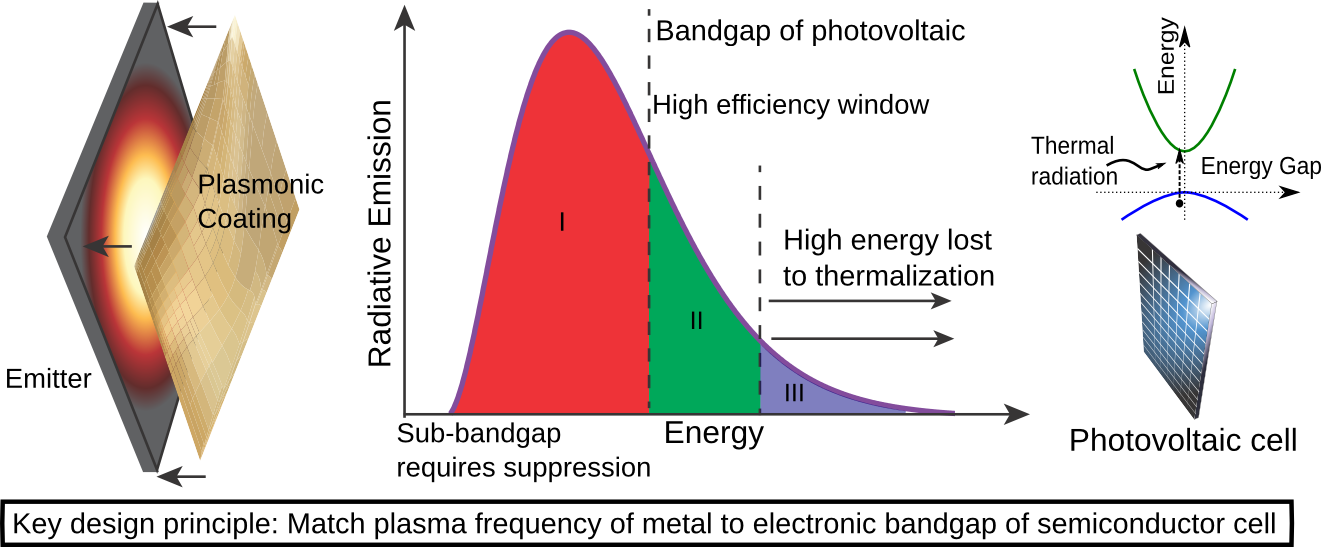
Thermophotovoltaic systems promise to provide high efficiency energy conversion from heat to electricity by spectrally matching the thermal emission from an emitter to the bandgap of a conventional single-junction photovoltaic cell Bauer (2011); Ilic et al. (2012a); Park et al. (2008); Nefzaoui et al. (2012); Molesky and Jacob (2015). This field of research has seen a resurgence in recent years due to parallel developments in the fields of nanoscale thermal engineering Nagasaka (2008), nanofabrication Fleming et al. (2003); Yeng et al. (2012) and high temperature material science Guler et al. (2014); Molesky et al. (2013); Guo et al. (2014); Nagpal et al. (2008). An important aspect of the thermophotovoltaic system is the design of the emitter, which has to suppress the thermal emission of sub-bandgap photons as they cannot be converted to electrical output Fleming et al. (2003); Yeng et al. (2012) and simultaneously enhance thermal emission just above the cell bandgap. Note that sub-bandgap blackbody photons are the primary reason for decrease in the efficiency of energy conversion (see Fig. 1). One necessary requirement for an emitter is robust optical response and thermal/structural stability of the emitter which has to withstand high temperatures Bauer (2011).
Significant recent advances have shown the potential of photonic crystals Fleming et al. (2003); Yeng et al. (2012); Nagpal et al. (2008); Rephaeli and Fan (2009); Narayanaswamy and Chen (2005); Celanovic et al. (2004) , thin films Guo et al. (2014); Wang et al. (2015); Song et al. (2015); Basu and Francoeur (2011); Edalatpour and Francoeur (2013); DiMatteo et al. (2001); Narayanaswamy and Chen (2003); Park et al. (2008); Joulain and Henkel (2008); Nefedov and Simovski (2011); Tong et al. (2015), perfect absorbers Tong et al. (2015), thermal metamaterials Dyachenko et al. (2016); Molesky et al. (2013); Mason et al. (2011); Liu et al. (2011); Wu et al. (2012), tungsten metasurfaces Zhao et al. (2013); Neuner III et al. (2013); Wu et al. (2012), graphene Messina and Ben-Abdallah (2012); Svetovoy and Palasantzas (2014), surface waves Ben-Abdallah et al. (2013); Joulain et al. (2005) and other nanophotonic structures Ilic et al. (2012a); Deng et al. (2015) to engineer the thermal emission Drevillon et al. (2011); Lee and Zhang (2007) and achieve spectrally selective emitters Drevillon et al. (2011); Wang et al. (2009); Lee and Zhang (2007). Simultaneously, work has progressed to advance the critical challenge involving the absorber/TPV cell design.
Here, we build on our previous work on the first suggestion of high temperature plasmonics Guo et al. (2014); Molesky et al. (2013) and experimental demonstration of high temperature thermal metamaterials Dyachenko et al. (2016). In this paper, we provide an alternative in selective emitter design employing only a single layer of plasmonic thermal emitter coating. This design holds the significant advantage of not requiring 2D patterning to achieve the desired optical response. Along with ease of large area fabrication it also opens up the possibility of high temperature stable operation since 2D texturing often reduces the melting point of metals. The primary objective of thermal suppression of sub-bandgap photons can be achieved by tuning the epsilon-near-zero (ENZ) frequency (also known as plasma frequency) of a metal to the bandgap of the cell. Thus natural material properties provide the reflectivity change desired for the thermal emitter as opposed to structural bandgap effects as in photonic crystals. We also show that our design is useful for engineering narrowband near-field thermal emission paving the way for a unified platform for both far-field and near-field thermal emitters. We also provide detailed performance analysis for our thin film designs. It should be noted that polar dielectric thin films (eg: silicon carbide) only show phonon-polaritonic resonances and epsilon-near-zero regime only in the mid-infrared frequency ranges and not in the near-infrared range conducive for high temperature thermophotovoltaic applications.
One important application of selective thermal emitters is the ability to modulate thermal emission along with spectrally selective nature Brar et al. (2015); Van Zwol et al. (2011); Fang et al. (2013); Freitag et al. (2010) . Graphene presents an ideal platform to achieve this effect due to the strong electrical tunability of its optical absorption properties Thongrattanasiri et al. (2012) . Graphene is expected to find wide applications in next generation electronic devices due to its good electrical Bolotin et al. (2008) and thermal properties Ghosh et al. (2008) and strong light matter interactions Koppens et al. (2011). A substrate coated with a graphene layer has been reported to have highly directive far-field thermal emission, enhanced light absorption Pu et al. (2013) and enhanced near-field radiation transfer Ilic et al. (2012b); Lim et al. (2013). An important emerging platform are the multilayer graphene based metamaterials Iorsh et al. (2013); Zhang et al. (2014); Sreekanth et al. (2013), which have been reported to exhibit tunable absorption and hyperbolic dispersion Othman et al. (2013); Linder and Halterman ; Chang et al. (2016).
In this paper, we report a sharp suppression in the thermal emissivity of graphene-multilayer structure, and show that it can be controlled by tuning the topological transition in the graphene metamaterial. We also report a sharp enhancement in the near-field thermal emission in graphene-multilayers due to topological transitions. These results forms a crucial step in the realization of thermal energy scavenging technologies in future graphene based electronic devices. We note that the opportunity to electrically tune topological transitions can be an important design principle for spectrally selective thermal modulation.
II High temperature plasmonic thermal emitter coating (p-TEC)
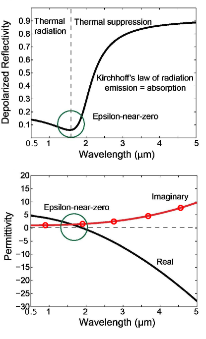
Selective thermal emitters for TPVs have to perform the important function of thermal suppression below the bandgap of the absorbing cell and simultaneously enhance emission just above the PV cell bandgap Rephaeli and Fan (2009); Lenert et al. (2014). We design this feature by employing a thin film of Drude metal with engineered plasma frequency (ENZ frequency) and no surface patterning. The plasma frequency is the characteristic frequency above which metals lose their reflectivity and become transparent. Thus metals absorb above the plasma frequency and reflect light below the plasma frequency. Fig. 2(a) and (b) show the correspondence between a sharp reflectivity change at normal incidence and the ENZ wavelength for a Drude metal. The high reflectivity leads to decreased optical absorption and suppresses the thermal emission by the Kirchoff’s law (absorptivity=emissivity). One can therefore achieve suppression of sub-bandgap thermal emission simply by tuning the plasma frequency in the near-infrared range close to the bandgap of the TPV cell. The design achieves enhancement in thermal emission in the transparency range of the metal tuned to be above the bandgap of the cell. Note, all metals are transparent and lossy above the ENZ frequency (plasma frequency) giving rise to large absorption and emission.
III High Temperature Material Properties
We now outline the choices for high temperature metals that can act as a plamonic thermal emitter coating. Even though tungsten and tantalum have excellent thermal propertiesLenert et al. (2014), the plasma frequency (ENZ frequency) cannot be tuned to the near-infared range to match the low energy bandgap of gallium antimonide or germanium TPV cells. We have performed detailed analysis of titanium nitride and zirconium nitride which are refractory metals with plasmonic response for TPV applications Guler et al. (2014); Li et al. (2014). Our analysis (to be published later) indicate that their interband transitions and losses, especially in the near-infrared region are sub-optimal for both the far-field and the near-field plasmonic thermal emitter performance. They will need to be optimized to find use in TPV systems as a thin film plasmonic coating but can be used as nanoantennas Guler et al. (2014); Li et al. (2014). In this work, we therefore focus on the use of aluminum doped zinc oxide (AZO) and gallium doped zinc oxide (GZO) with plasma frequency (ENZ frequency) tuned in the near-infrared for p-TECs Pradhan et al. (2014); Kim et al. (2013). In general, the optical response of materials at high temperatures poses a significant challenge for thermal emitter design. We have utilized empirical models of tungsten and AZO/GZO available in literature to arrive at general conclusions of the real part and imaginary part of the response at high temperatures Pradhan et al. (2014); Kim et al. (2013); Krishnamoorthy et al. (2012); Naik et al. (2011); Roberts (1959); Costescu et al. (2003); Schmid et al. (1998); Larruquert et al. (2012); Liu et al. (2015). Increasing temperature causes a rise in electron-phonon interactions and simultaneous reduction of collision time. This is manifested in a reduction of the bulk polarization response and increase in optical absorption. Consequently, the real part of the dielectric constant governing the polarization response is reduced and the imaginary part of the dielectric constant governing losses is increased. Thus the performance of plasmonic components is expected to be reduced at high temperature. A detailed analysis of these empirical models will be published later.
IV High temperature thermal emission suppression
IV.1 Far-field thermal emission: thin-film AZO and other approaches
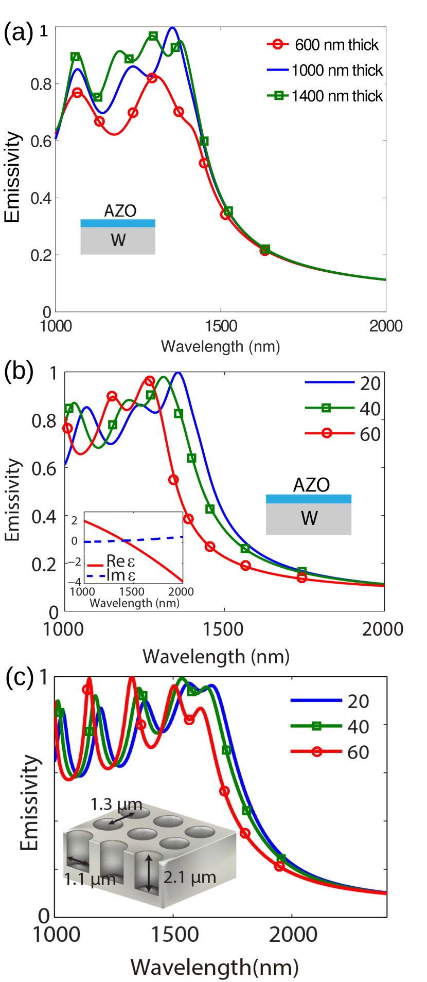
We now provide the results of calculations using an AZO plasmonic thermal emitter coating. Using Kirchhoff’s laws Greffet and Nieto-Vesperinas (1998), we calculate the emissivity of an AZO film of thickness 600 nm, 1000 nm and 1400 nm, placed on a tungsten substrate (Fig. 3(a)). It can be observed that there is a sharp suppression in the emissivity above ENZ wavelength of 1400 nm, irrespective of the thickness of the AZO film. This is because the spectral thermal emission response is dominated by the material properties of the AZO and the thickness only effects the ripples in the high emissivity region. Fig. 3(b) shows the emissivity of a 1000 nm thick AZO film at different emission angles. The inset shows the real and imaginary part of AZO dielectric response. The emissivity performance at different emission angles displays a similar cut-off behavior, which is necessary for TPV applications. The p-TEC (Fig. 3(b)) achieves an emissivity profile very close to a tungsten photonic crystal (PhC) design (Fig. 3(c)). However, note that there are fundamental differences in the approach to achieving thermal suppression. The PhC utilizes a structural resonance and interference effects whereas the p-TEC uses an engineered material response. A simple thin-film coating with engineered material response matches the performance of a microfabricated photonic crystal.
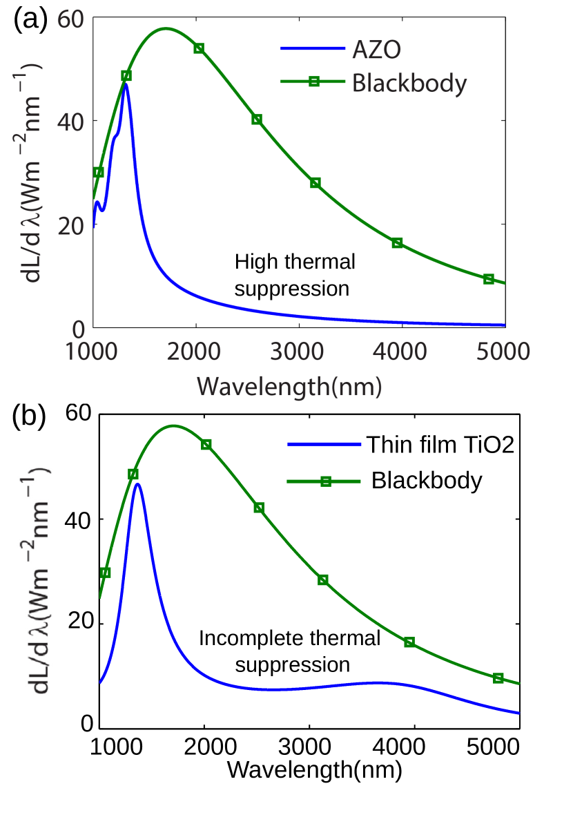
Thin-film p-TEC with engineered material response also outperforms thin-film anti-reflection coatings. Fig. 4 compares the performance of an anti-reflection coating (AR) Fraas et al. (2001) as a selective thermal emitter. Fig. 4(a) shows the spectral irradiance from an AZO coated tungsten substrate at 1700K. On comparison with black body radiation, it can be clearly seen that the thermal radiation in the sub-bandgap region is suppressed. This sharp suppression at high wavelengths is because the emissivity of AZO coating drops above the epsilon-near-zero wavelength. The thickness of the the AZO film is 1000 nm. Fig. 4(b) shows the thermal radiation from a tungsten coated with TiO2 AR coating. Enhancement in the thermal emission near 1500 nm wavelength in AR coating is due to the enhanced absorptivity arising from Fabry-Perot resonance mode in a TiO2 film of thickness 355 nm. The peak emittance in TiO2 can therefore be tuned by tuning the thickness of AR coating. This is in contrast to the AZO thin film, where the suppression in the emissivity is governed by the material response while the thickness has only a minor effect on the emissivity at transparent low-wavelength region of the spectrum. It can be seen that the even at sub-bandgap wavelengths, the thermal emission in TiO2 is considerably larger as compared to the AZO coating. The incomplete thermal suppression in AR coating degrades its efficiency performance.
To provide a performance comparison in the limiting ideal case of these various emitter designs for TPV applications, we apply the Schockley-Queisser detailed balance analysis Rephaeli and Fan (2009). In performing this calculation we assume the photovoltaic cell in all cases to be a perfectly absorbing, ideal pn-junction, with a bandgap of 2250 nm for the photonic crystal emitter and 1700 nm for the AZO plasmonic coating and titanium dioxide anti-reflection coating designs. We also assume that the emitter and photovoltaic cell have the same flat area, and that no absorbing stage is present. Under these conditions, the conversion efficiency of radiated thermal energy into electrical energy in AZO, photonic crystal and TiO2 coating is shown in Table 1. The efficiency of a simple AZO thin-film is less then, but comparable with the photonic crystal spectrally selective emitter, while it outperforms the TiO2 thin film. The poor efficiency of TiO2 is because of incomplete thermal suppression at higher wavelengths.
| Temperature | AZO thin-film | Photonic crystal | TiO2 |
|---|---|---|---|
| 1700K | 31.9 % | 36.7 % | 19.6 % |
| 1300K | 19.4 % | 29.1 % | 9.2 % |
IV.2 Narrow-band near-field thermal emission
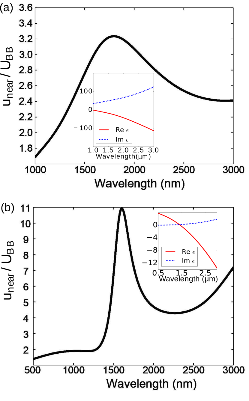
A fundamental advantage of the p-TEC design is that it can simultaneously be used as a near-field emitter and can exhibit narrowband near-field thermal emission. This arises due to thin film surface plasmon polaritons excited at high temperatures which lead to narrowband thermal emission with potential applications for near-field TPV. While fundamentally challenging to implement, near-field TPVs promises to achieve high efficiency of conversion with high current densitiesBasu and Zhang (2009). This is because near-field thermal energy transfer mediated by evanescent waves can exceed the far-field black body limit.
In Fig. 5(a), we plot the energy density in the near-field of a conventional emitter used in near-field TPV designs consisting of a thin film of tungsten. The energy density is normalized to that of a black body in the far-field and calculated using Rytov’s fluctuational electrodynamicsNagasaka (2008); Liu et al. (2015). The energy density at a distance and frequency is Joulain (2007)
where denotes the temperature. , , (such that ), and are the Fresnel reflection coefficients from the thin films for (s) and (p) polarized light respectively and “” denotes the imaginary part. is the black body emission spectrum. The near-field energy density enhancement is due to the excitation of weak and lossy surface waves in highly absorptive tungsten (above its plasma wavelength of ). Due to the lossy nature of tungsten at near-infrared wavelengths Roberts (1959), the enhancement is low, with a broad spectrum. This poor spectral performance is a significant limiting factor for TPVs.
Fig. 5(b) shows the near-field energy density near a thin film of Gallium doped Zinc-oxide (GZO). The plasma frequency (ENZ frequency) of doped zinc-oxide can be tuned to be in the near-infrared spectral range, matched to the bandgap of a TPV cell (GaSb). The spectrally selective nature along with the larger enhancement of near-field energy density, evident in Fig.5(b), is due to the excitation of surface plasmons. By controlling the film thickness and ENZ permittivity of the GZO film, the spectral content of near-field enhancement can tuned to match the high efficiency window of energies directly above the band-gap of a PV cell. For comparison, the thickness of tungsten and gallium doped-zinc-oxide are selected such that the peak in energy density enhancement is optimized at the same frequency. The plasmonic thermal emitter coating (p-TEC) outperforms the thin film of tungsten and can be used in both near-field and far-field TPV.
V Thermal topological transitions in graphene multilayers
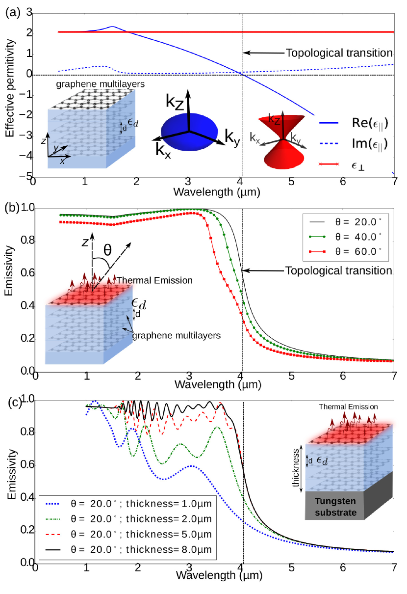
Thermal emission can also be engineered by controlling the topological transition in a graphene-multilayer structure. A schematic of the graphene multilayers stacked between dielectric slabs of and thickness nm is shown in inset of Fig. 6(a). The layers are stacked along the direction. A multilayer structure thus formed has an anisotropic dielectric tensor, whose perpendicular component (along the -direction) of the permittivity () is given by the dielectric , while the parallel component (, parallel to the layers in plane) is governed a combination of three factors: (i) the complex conductivity of graphene, (ii) the thickness of the separating substrate () and (iii) the dielectric . The equations for computing the dielectric tensor of graphene metamaterial is presented in Appendix. Fig. 6(a) shows the parallel component (in plane) and the perpendicular component (along -direction) of the dielectric tensor, when Fermi energy of each graphene layer is eV. It can be seen that the parallel component of permittivity changes sign from positive to negative around 4.05 m, triggering a topological transition from elliptical to hyperbolic iso-frequency surface, as shown in the inset. At the topological transition wavelength, the emissivity of the structure drops sharply due to large miss-match in the hyperbolic topology of the graphene-multilayer substrate and the elliptical topology of the free-space. Fig. 6(b) shows the suppression of emissivity at different angles from bulk graphene metamaterial. For thermal emission applications the graphene metamaterial substrate will need to be deposited on a substrate, such as tungsten. Fig. 6(c) shows the emission characteristics of graphene metamaterial deposited on tungsten substrate for varying thickness of the graphene-multilayer. It can be seen that as the thickness increases beyond 5 m, its emission characteristics approach those of the bulk graphene. These computations are done for a Fermi-energy of 0.4 eV.
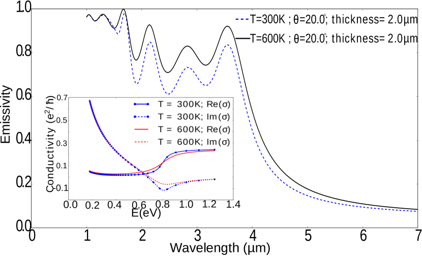
We would like to point out that the wavelength at which topological transition in graphene metamaterial occurs can be controlled by the dielectric thickness as well as the Fermi energy of the individual graphene sheets. This gives us an additional degree of freedom in controlling the topological transition wavelength. The graphene metametrial is also suited for high temperature applications as its doping concentration and complex conductivity is does not vary substantially with temperature Fang et al. (2015). Fig. 7 shows the variation in emissivity at temperature T=300K and T=600K. The change in complex conductivity of individual graphene sheets at the two temperatures is shown as inset. It can be seen that the even at a higher temperature, the emissivity of the graphene metamaterial is suppressed at higher wavelengths.
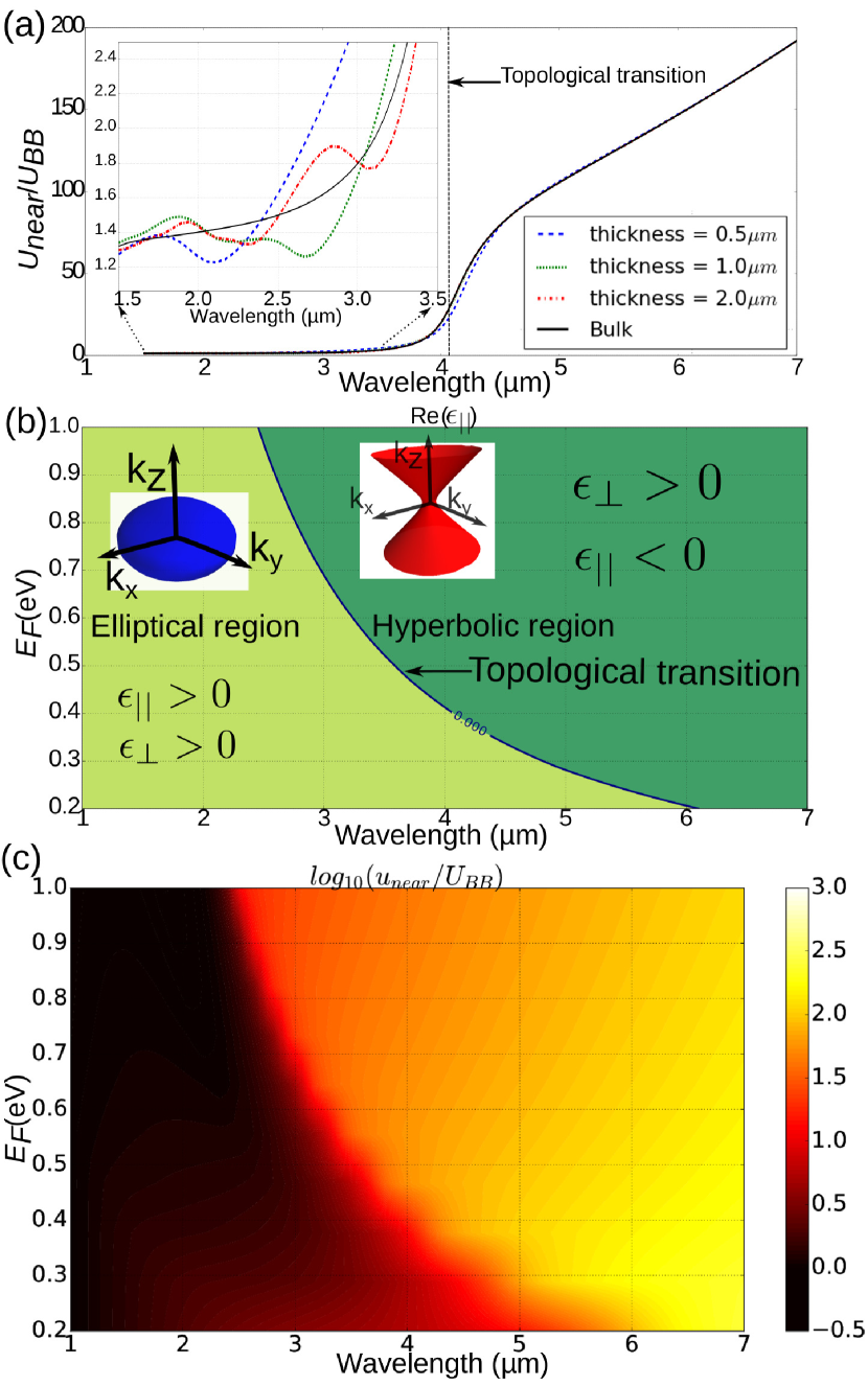
The topological transition in graphene-multilayers also results in enhanced near-field thermal emission. Graphene multilayers support unbounded bulk hyperbolic states which increase the local density of states in vacuum, near the surface. This increased local density of states results in enhanced near-field energy density and near-field thermal emission. Fig. 8(a) shows the large enhancement in the near-field energy density (normalized to that of black body), in the hyperbolic region of the spectrum. It can be observed that there is a sharp increase in energy density at the topological transition wavelength. The near-field energy is computed for increasing thickness of graphene-multilayer on a tungsten substrate. It can be seen in the zoomed-in inset that the finite thickness has small effect on the near-field as compared to large enhancement triggered by topological transition. The near-field energy is computed at a distance of 100 nm from the substrate. The topological transition and hence the near-field emission can be tuned by controlling the Fermi energy of the graphene layers. The contour on which the topological transition occurs as function of wavelength and Fermi-energy is shown in Fig. 8(b). The corresponding enhancement in the thermal emission at K is shown in Fig. 8(c). It is evident that the enhancement in near-field energy density is triggered at the topological transition for all values of Fermi energy.
VI Summary
In conclusion, we have introduced the concept of a plasmonic thermal emitter coating. It functions on the basis of reflectivity change of metallic thin films near the epsilon-near-zero frequency. Our approach shows superior performance as compared to anti-reflection coatings and is easier to fabricate than photonic crystals which require 2D surface patterning of tungsten. We have shown that it achieves narrowband thermal emission in the near-field as compared to tungsten. Developments in high temperature plasmonics can make our thin film design a viable large area technology for thermal emitters. We have also shown that the thermal topological transitions in graphene multilayers can lead to tunable spectrally selective thermal emission.
Acknowledgements
We acknowledge funding from Alberta Innovates Technology Futures, NSERC, Helmholtz Alberta Initiative and NSF EFRI NEWLAW.
Appendix A Thermal emission from Fluctuation Dissipation Theorem
Any material consists of a large ensemble of fluctuating currents which are the source of thermal radiation. The Poynting vector of the thermal radiation from a from a material is governed by the Fluctuation Dissipation Theorem. The thermal radiation from a material half-space, in the -direction, is given by Joulain (2007),
| (1) |
where is the angle from the normal (-axis) to the interface, and is the emissivity of the material, given by,
| (2) |
where, and is the reflection coefficient of and polarized wave at the interface of the material and vacuum.
We numerically compute the reflection coefficient at the vacuum/thin-film interface for a and polarized wave. These reflection coefficients as a function of frequency and incident angles are then used to compute the far-field and near-field thermal emission.
Appendix B Effective permittivity of graphene-multilayers
| (3) |
where,
| (4) |
and
| (5) |
Relaxation time s, is temperature in Kelvin. Where and corresponds to intra-band and inter-band conductivity, respectively; is the Boltzmann constant, and is the Fermi Energy.
When the graphene multilayers are stacked between material of dielectric constant and thickness (as shown in inset of Fig. 6(a)), the resultant material is anisotropic, with dielectric tensor,
| (6) |
where and are the and component of the effective dielectric, respectively Chang et al. (2016).
| (7) | |||||
| (8) |
For computation of thermal emission from graphene metamaterial, the reflection coefficients are computed for film of anisotropic dielectric tensor given by equation (6).
References
- Bauer (2011) T. Bauer, Thermophotovoltaics: basic principles and critical aspects of system design (Springer Science & Business Media, 2011).
- Ilic et al. (2012a) O. Ilic, M. Jablan, J. D. Joannopoulos, I. Celanovic, and M. Soljačić, Optics express 20, A366 (2012a).
- Park et al. (2008) K. Park, S. Basu, W. P. King, and Z. Zhang, Journal of Quantitative Spectroscopy and Radiative Transfer 109, 305 (2008).
- Nefzaoui et al. (2012) E. Nefzaoui, J. Drevillon, and K. Joulain, Journal of Applied Physics 111, 084316 (2012).
- Molesky and Jacob (2015) S. Molesky and Z. Jacob, Physical Review B 91, 205435 (2015).
- Nagasaka (2008) Y. Nagasaka, International Journal of Thermophysics 29, 787 (2008).
- Fleming et al. (2003) J. G. Fleming, S.-Y. Lin, and J. B. Moreno, A three-dimensional photonic-crystal emitter for thermal photovoltaic power generation., Tech. Rep. (Sandia National Laboratories, 2003).
- Yeng et al. (2012) Y. X. Yeng, M. Ghebrebrhan, P. Bermel, W. R. Chan, J. D. Joannopoulos, M. Soljačić, and I. Celanovic, Proceedings of the National Academy of Sciences 109, 2280 (2012).
- Guler et al. (2014) U. Guler, A. Boltasseva, and V. M. Shalaev, Science 344, 263 (2014).
- Molesky et al. (2013) S. Molesky, C. J. Dewalt, and Z. Jacob, Optics express 21, A96 (2013).
- Guo et al. (2014) Y. Guo, S. Molesky, H. Hu, C. L. Cortes, and Z. Jacob, Applied Physics Letters 105, 073903 (2014).
- Nagpal et al. (2008) P. Nagpal, S. E. Han, A. Stein, and D. J. Norris, Nano letters 8, 3238 (2008).
- Rephaeli and Fan (2009) E. Rephaeli and S. Fan, Optics express 17, 15145 (2009).
- Narayanaswamy and Chen (2005) A. Narayanaswamy and G. Chen, Journal of Quantitative Spectroscopy and Radiative Transfer 93, 175 (2005).
- Celanovic et al. (2004) I. Celanovic, F. O’Sullivan, N. Jovanovic, M. Qi, and J. G. Kassakian, in Photonics Europe (International Society for Optics and Photonics, 2004) pp. 416–422.
- Wang et al. (2015) Z. Wang, T. S. Luk, Y. Tan, D. Ji, M. Zhou, Q. Gan, and Z. Yu, Applied Physics Letters 106, 101104 (2015).
- Song et al. (2015) B. Song, Y. Ganjeh, S. Sadat, D. Thompson, A. Fiorino, V. Fernández-Hurtado, J. Feist, F. J. Garcia-Vidal, J. C. Cuevas, P. Reddy, et al., Nature nanotechnology 10, 253 (2015).
- Basu and Francoeur (2011) S. Basu and M. Francoeur, Applied Physics Letters 98, 243120 (2011).
- Edalatpour and Francoeur (2013) S. Edalatpour and M. Francoeur, Journal of Quantitative Spectroscopy and Radiative Transfer 118, 75 (2013).
- DiMatteo et al. (2001) R. S. DiMatteo, P. Greiff, S. L. Finberg, K. A. Young-Waithe, H. Choy, M. M. Masaki, and C. G. Fonstad, Applied Physics Letters 79, 1894 (2001).
- Narayanaswamy and Chen (2003) A. Narayanaswamy and G. Chen, Applied Physics Letters 82, 3544 (2003).
- Joulain and Henkel (2008) K. Joulain and C. Henkel, Applied Physics B 93, 151 (2008).
- Nefedov and Simovski (2011) I. S. Nefedov and C. R. Simovski, Physical Review B 84, 195459 (2011).
- Tong et al. (2015) J. K. Tong, W.-C. Hsu, Y. Huang, S. V. Boriskina, and G. Chen, Scientific reports 5 (2015).
- Dyachenko et al. (2016) P. Dyachenko, S. Molesky, A. Y. Petrov, M. Störmer, T. Krekeler, S. Lang, M. Ritter, Z. Jacob, and M. Eich, Nature communications 7 (2016).
- Mason et al. (2011) J. Mason, S. Smith, and D. Wasserman, Applied Physics Letters 98, 241105 (2011).
- Liu et al. (2011) X. Liu, T. Tyler, T. Starr, A. F. Starr, N. M. Jokerst, and W. J. Padilla, Physical review letters 107, 045901 (2011).
- Wu et al. (2012) C. Wu, B. Neuner III, J. John, A. Milder, B. Zollars, S. Savoy, and G. Shvets, Journal of Optics 14, 024005 (2012).
- Zhao et al. (2013) B. Zhao, L. Wang, Y. Shuai, and Z. M. Zhang, International Journal of Heat and Mass Transfer 67, 637 (2013).
- Neuner III et al. (2013) B. Neuner III, C. Wu, G. Ten Eyck, M. Sinclair, I. Brener, and G. Shvets, Applied Physics Letters 102, 211111 (2013).
- Messina and Ben-Abdallah (2012) R. Messina and P. Ben-Abdallah, Scientific reports 3, 1383 (2012).
- Svetovoy and Palasantzas (2014) V. Svetovoy and G. Palasantzas, Physical Review Applied 2, 034006 (2014).
- Ben-Abdallah et al. (2013) P. Ben-Abdallah, F. Marquier, and J.-J. Greffet, in Plasmonics: Theory and Applications (Springer, 2013) pp. 283–327.
- Joulain et al. (2005) K. Joulain, J.-P. Mulet, F. Marquier, R. Carminati, and J.-J. Greffet, Surface Science Reports 57, 59 (2005).
- Deng et al. (2015) H. Deng, Z. Li, L. Stan, D. Rosenmann, D. Czaplewski, J. Gao, and X. Yang, Optics letters 40, 2592 (2015).
- Drevillon et al. (2011) J. Drevillon, K. Joulain, P. Ben-Abdallah, and E. Nefzaoui, Journal of Applied Physics 109, 034315 (2011).
- Lee and Zhang (2007) B. Lee and Z. Zhang, Journal of Heat Transfer 129, 17 (2007).
- Wang et al. (2009) L. Wang, B. Lee, X. Wang, and Z. Zhang, International Journal of Heat and Mass Transfer 52, 3024 (2009).
- Brar et al. (2015) V. W. Brar, M. C. Sherrott, M. S. Jang, S. Kim, L. Kim, M. Choi, L. A. Sweatlock, and H. A. Atwater, Nature communications 6 (2015).
- Van Zwol et al. (2011) P. Van Zwol, K. Joulain, P. B. Abdallah, J.-J. Greffet, and J. Chevrier, Physical Review B 83, 201404 (2011).
- Fang et al. (2013) Z. Fang, Y. Wang, A. E. Schlather, Z. Liu, P. M. Ajayan, F. J. García de Abajo, P. Nordlander, X. Zhu, and N. J. Halas, Nano letters 14, 299 (2013).
- Freitag et al. (2010) M. Freitag, H.-Y. Chiu, M. Steiner, V. Perebeinos, and P. Avouris, Nature nanotechnology 5, 497 (2010).
- Thongrattanasiri et al. (2012) S. Thongrattanasiri, F. H. Koppens, and F. J. G. de Abajo, Physical review letters 108, 047401 (2012).
- Bolotin et al. (2008) K. I. Bolotin, K. Sikes, Z. Jiang, M. Klima, G. Fudenberg, J. Hone, P. Kim, and H. Stormer, Solid State Communications 146, 351 (2008).
- Ghosh et al. (2008) S. Ghosh, I. Calizo, D. Teweldebrhan, E. Pokatilov, D. Nika, A. Balandin, W. Bao, F. Miao, and C. N. Lau, Applied Physics Letters 92, 151911 (2008).
- Koppens et al. (2011) F. H. Koppens, D. E. Chang, and F. J. Garcia de Abajo, Nano letters 11, 3370 (2011).
- Pu et al. (2013) M. Pu, P. Chen, Y. Wang, Z. Zhao, C. Wang, C. Huang, C. Hu, and X. Luo, Optics express 21, 11618 (2013).
- Ilic et al. (2012b) O. Ilic, M. Jablan, J. D. Joannopoulos, I. Celanovic, H. Buljan, and M. Soljačić, Physical Review B 85, 155422 (2012b).
- Lim et al. (2013) M. Lim, S. S. Lee, and B. J. Lee, Optics express 21, 22173 (2013).
- Iorsh et al. (2013) I. V. Iorsh, I. S. Mukhin, I. V. Shadrivov, P. A. Belov, and Y. S. Kivshar, Physical Review B 87, 075416 (2013).
- Zhang et al. (2014) L. Zhang, Z. Zhang, C. Kang, B. Cheng, L. Chen, X. Yang, J. Wang, W. Li, and B. Wang, Optics express 22, 14022 (2014).
- Sreekanth et al. (2013) K. Sreekanth, A. De Luca, and G. Strangi, Applied Physics Letters 103, 023107 (2013).
- Othman et al. (2013) M. A. Othman, C. Guclu, and F. Capolino, Optics express 21, 7614 (2013).
- (54) J. Linder and K. Halterman, Scientific Reports 6.
- Chang et al. (2016) Y.-C. Chang, C.-H. Liu, C.-H. Liu, S. Zhang, S. R. Marder, E. E. Narimanov, Z. Zhong, and T. B. Norris, Nature communications 7 (2016).
- Lenert et al. (2014) A. Lenert, D. M. Bierman, Y. Nam, W. R. Chan, I. Celanović, M. Soljačić, and E. N. Wang, Nature nanotechnology 9, 126 (2014).
- Li et al. (2014) W. Li, U. Guler, N. Kinsey, G. V. Naik, A. Boltasseva, J. Guan, V. M. Shalaev, and A. V. Kildishev, Advanced Materials 26, 7959 (2014).
- Pradhan et al. (2014) A. Pradhan, R. Mundle, K. Santiago, J. Skuza, B. Xiao, K. Song, M. Bahoura, R. Cheaito, and P. E. Hopkins, Scientific reports 4 (2014).
- Kim et al. (2013) J. Kim, G. V. Naik, A. V. Gavrilenko, K. Dondapati, V. I. Gavrilenko, S. Prokes, O. J. Glembocki, V. M. Shalaev, and A. Boltasseva, Physical Review X 3, 041037 (2013).
- Krishnamoorthy et al. (2012) H. N. Krishnamoorthy, Z. Jacob, E. Narimanov, I. Kretzschmar, and V. M. Menon, Science 336, 205 (2012).
- Naik et al. (2011) G. V. Naik, J. Kim, and A. Boltasseva, Optical Materials Express 1, 1090 (2011).
- Roberts (1959) S. Roberts, Physical Review 114, 104 (1959).
- Costescu et al. (2003) R. M. Costescu, M. A. Wall, and D. G. Cahill, Physical Review B 67, 054302 (2003).
- Schmid et al. (1998) P. E. Schmid, M. S. Sunaga, and F. Lévy, Journal of Vacuum Science & Technology A 16, 2870 (1998).
- Larruquert et al. (2012) J. I. Larruquert, A. P. Pérez-Marín, S. García-Cortés, L. Rodríguez-de Marcos, J. A. Aznárez, and J. A. Méndez, JOSA A 29, 117 (2012).
- Liu et al. (2015) X. Liu, B. Zhao, and Z. M. Zhang, Physical Review A 91, 062510 (2015).
- Greffet and Nieto-Vesperinas (1998) J.-J. Greffet and M. Nieto-Vesperinas, JOSA A 15, 2735 (1998).
- Fraas et al. (2001) L. M. Fraas, J. E. Samaras, and J. E. Avery, “Antireflection coated refractory metal matched emitters for use in thermophotovoltaic generators,” (2001), uS Patent 6,271,461.
- Basu and Zhang (2009) S. Basu and Z. Zhang, Journal of Applied Physics 105, 093535 (2009).
- Joulain (2007) K. Joulain, in Microscale and nanoscale heat transfer (Springer, 2007) pp. 107–131.
- Fang et al. (2015) X.-Y. Fang, X.-X. Yu, H.-M. Zheng, H.-B. Jin, L. Wang, and M.-S. Cao, Physics Letters A 379, 2245 (2015).
- Wunsch et al. (2006) B. Wunsch, T. Stauber, F. Sols, and F. Guinea, New Journal of Physics 8, 318 (2006).
- Hwang and Sarma (2007) E. Hwang and S. D. Sarma, Physical Review B 75, 205418 (2007).