Exciton Transfer in Array of Epitaxially Connected Nanocrystals
Abstract
Recently, epitaxially connected at facets semiconductor nanocrystals (NCs) have been introduced to fascilitate the electron transport between nanocrystals. To fully deploy their potential a better understanding of the exciton transfer between connected NCs is needed. We go beyond the two well-known transfer mechanisms suggested by Förster and Dexter and propose a third mechanism of exciton tandem tunneling. The tandem tunnelling occurs through the intermediate state in which electron and hole are in different NCs. The corresponding rate for exciton hops is larger than the Dexter rate and for Si is even much larger that the Förster one.
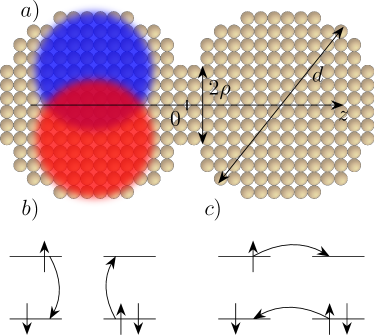
Semiconductor nanocrystals (NCs) have shown great potential in optoelectronics applications such as solar cells Shirasaki et al. (2012); Liu et al. (2009); Gur et al. (2005), light-emitting diodes Yang et al. (2015); Gong et al. (2016); Bae et al. (2013), field-effect transistors Straus et al. (2015); Choi et al. (2012); Reich et al. (2014); Liu et al. (2013); Choi et al. (2016) and mid-infrared detectors Keuleyan et al. (2011); Jeong and Guyot-Sionnest (2016) by virtue of their size-tunable optical and electrical properties and low-cost solution-based processing techniques Talapin et al. (2010). As grown NCs are covered by ligands which deplete conductivity of NC arrays. For applications one needs a good electronic transport in a NC array. Substantial improvement of the transport properties of a NC array was achieved by replacing of long ligands with shorter ones Kagan and Murray (2015); Choi et al. (2012); Liu et al. (2013, 2013). Recent progress Lanigan and Thimsen (2016); Oh et al. (2014); Delerue (2016); Williams et al. (2009); Delerue (2016); Walravens et al. (2016); Baumgardner et al. (2013); Sandeep et al. (2014); Li et al. (2016) lead to the creation of NCs which touch each other by facets or are epitaxially connected and as a result demonstrate good conductivity Whitham et al. (2016); Evers et al. (2015); Jang et al. (2015). Fig. 1a shows an example of two NCs epitaxially connected at a facet with a small contact radius NCs. Electron tunneling through a small facet leading to variable range hopping of electrons in doped NC array was studied theoretically Fu et al. (2016) and the criterium of the insulator-metal transition was derived Chen et al. (2016). The transition was approached via doping of NCs Chen et al. (2016) or crossed via increasing contact radius Lanigan and Thimsen (2016).
In optical devices based on NC arrays absorption of a light quantum results in the creation of an exciton (a bound electron-hole pair) in a NC. An exciton can hop between nearest neighbour NCs. Corresponding diffusion coefficient and diffusion length were studied experimentally Kagan et al. (1996); Crooker et al. (2002); Miyazaki and Kinoshita (2012); Achermann et al. (2003); Kholmicheva et al. (2015); Poulikakos et al. (2014); Crisp et al. (2013). The diffusion length of excitons sets the volume from which the light energy is harvested in solar cells . Thus, the mechanism of exciton transfer between NCs is central to a NC device design. This paper addresses exciton hopping between nearest epitaxially connected NCs.
In a typical array NCs have slightly different diameters and therefore excitons have different ground state energies. At low temperatures an exciton hops from a small NC to a larger one, where its energy is smaller. This leads to a red shift of photoluminscence Kagan et al. (1996). On the other hand, at larger temperatures an exciton can hop Kholmicheva et al. (2015) even from a larger NC to a smaller one with absorption of a phonon. In both cases the exciton transfer rate between two nearest-neighbor NCs is determined by the Fermi golden rule and is proportional to the square of the matrix element for the exciton transfer . ( is the energy splitting between symmetric and antisymmetric states of two resonance nearest neighbor NCs.) In this work we concentrate on this matrix element. It is known that an exciton can hop from one NC to another via dipole-dipole Förster mechanism Kagan et al. (1996); Mork et al. (2014); Akselrod et al. (2014) (see Fig. 1b). This mechanism does not require tunneling of an electron or a hole between NCs and, therefore, dominates when NCs are separated by long ligands. Epitaxial connection of NCs via small facet with radius (see Fig. 1a) does not change the Förster rate. On the other hand, tunneling of electrons and holes between epitaxially connected NCs opens additional possibilities for the exciton transfer.
To describe them we assume that a NC is almost a sphere of diameter . In an isolated NC the electron and hole wave functions vanish at the NC surface, due to a large confining potential barriers created by the insulator matrix surrounding each NC. Under these conditions the ground state kinetic energy of an electron and hole is
| (1) |
where are the effective masses of an electron and hole. The Coulomb energy
| (2) |
where is the effective dielectric constant of the NC array is another important energy scale. For all NCs with one finds , so we concentrate on this case.
In this paper we deal with epitaxially connected NCs and propose a mechanism where the electron and hole tunnel through the small contact facet in tandem. This happens in the second order perturbation theory through the intermediate state with energy in which the electron is already in the right NC, while the hole is still in the left NC. We show below that is very close to unity. The matrix element of the tandem tunneling is
| (3) |
where
| (4) |
are matrix elements for the electron and hole single particle tunneling through epitaxial connection from one NC to another, respectively. Eq. (4) was implicitly derived in Ref. Fu et al. (2016) and because of important role of in our theory we repeat its derivation below.
Let us formulate conditions at which our theory is applicable. We consider the case when an exciton does not dissociate. An exciton ionization requires energy larger than because two distant charged NCs are created from the neutral background. Thus, we consider low temperatures , when excitons are not thermally ionized. Diameters of a NC typically vary by , where Murray et al. (2000). This leads to variation of the electron energy by . We assume that , so that electron and hole cannot move separately. We also assume that , so that . In this situation electrons, holes and excitons are localized in their NCs. The opposite case , when electrons and holes are delocalized in the NC array was studied in Refs. Kalesaki et al. (2014, 2013); Beugeling et al. (2015).
Thus, we deal with the situation where
| (5) |
Energies are estimated for the wide class of NC materials in Table 1, where we see that all our conditions Eq. (5) are fulfilled (although sometimes only marginally). As shown in Table 1 for majority of materials the tandem tunneling exciton transfer rate is larger than the Dexter rate. For Si it is even much larger than Förster rate.
| NC | |||||||||
| InP | 0.1 | 9.6 | 7 | 490 | 50 | 60 | 3 | 0.2 | |
| CdSe | 0.16 | 9.5 | 5 | 400 | 40 | 60 | 3 | 0.1 | |
| ZnO | 0.26 | 3.7 | 2 | 140 | 15 | 150 | 1 | 0.05 | |
| Si | 0.22 | 12 | 0.4 | 150 | 15 | 50 | 1 | 10 |
I Results and Discussion
Let us first formulate our results. We show that in epitaxially connected array of NCs, the ratio between the tandem tunneling and Förster rates is
| (6) |
Here is the unconventional effective exciton Bohr radius, is the dipole moment matrix element taken between the valence- and conduction-band states and is the high frequency dielectric constant of the material.
In the Table 1 we summarize our estimates of the ratio (6) for different NCs. We used and . Values of are taken from Ref. Madelung (2013). For epitaxially connected NCs we use (see Ref. Reich and Shklovskii (2016)).
The ratio (6) is derived for materials with an isotropic single band hole and electron masses. For most materials the spectra are more complex. Below we explain how we average the masses for these materials and also how we calculate .
We see that, the tandem tunneling can be comparable with the Förster mechanism in semiconductors like InP, CdSe where the effective mass is small. The tandem tunneling can be more efficient in cases where the Förster mechanism is forbidden. For example, in indirect band gap semiconductors like Si, where is small and the Förster mechanism is not effective, the tandem tunneling mechanism dominates.
In another situation the tandem tunneling dominates at low temperatures. Excitons can be in bright or dark spin states Nirmal et al. (1995). Only the bright exciton can hop due to the Förster mechanism. The dark exciton has smaller energy and the dark-bright exciton splitting is of the order of a few meV. So at small temperatures an exciton is in the dark state and cannot hop by the Förster mechanism. At the same time the tandem tunneling is not affected by a spin state of an exciton.
Dexter Dexter (1953) suggested another exciton transfer mechanism which also is not affected by spin state of an exciton. Two electrons of two NCs exchange with each other (see Fig. 1c). We show below that for an array of NCs the ratio between rates for tandem tunneling and the Dexter mechanism is:
| (7) |
In most cases and as one can see from Table 1 that the tandem tunneling rate is much larger than the Dexter rates with the exception of ZnO.
It is worth noting that the same ratio holds not only for epitaxially connected NCs but for NCs separated by ligands. Of course, if NCs are separated by ligands say by distance and wave functions decay in ligands as , where is the decay length of an electron outside of a NC, both rates acquire additional factor . Also, the difference between the tandem mechanism and Dexter transfer emerges only in NCs, where . In atoms and molecules, where essentially there is no such difference between the two mechanisms.
For epitaxially connected Si and InP NCs where the tandem tunneling is substantial these predictions can be verified in the following way. One can transform the bright exciton to the dark one by varying magnetic field or temperature. The exciton in the dark state cannot hop by the Förster mechanism, and usually hops much slower Liu et al. (2015); Blumling et al. (2012). For epitaxially connected NCs, where the tandem rate is larger than the Förster one the exciton transfer should not be affected by magnetic field or temperature.
Let us switch to derivation of the main result. For that we first should discuss electron wave functions in epitaxially connected NCs.
Wave functions of two epitaxially connected NCs. Below we describe the envelope wave functions in two epitaxially connected NCs. Here we present only scaling estimates and calculate numerical coefficients in the methods section. The wave functions for electrons and holes are the same, so we concentrate only on the electron. In an isolated NC the electron wave function is:
| (8) |
where is the distance from the center of the NC. We focus on two NCs shown on Fig 1, which touch each other by the small facet in the plane . In this situation the wave function for an electron in the left NC leaks through this small facet, so that it is finite in the plane of the facet and in the right NC. The derivative is hardly changed by this small perturbation, so that the wave function in the plane acquires a finite value:
| (9) |
The same happens with the wave functions of an electron in the right NC . and are symmetric with respect to the plane .
Tunneling matrix element. We calculate the matrix element (3) of an electron and hole tunneling through the contact facet in the second order perturbation theory. is the energy of the intermediate state, in which the electron moves to the right NC, while the hole is still in the left NC. In other words the left NC plays the role of donor (D) and the right one the role of acceptor (A) so that intermediate state is state. For touching NCs the energy of state is evaluated in the methods section and is shown to be , where . Therefore in Eq. (3) and through out the paper we use . In Eq. (3) factor takes care about two possible orders of electron and hole hops.
Matrix elements for the electron and hole single particle tunneling from one NC to another can be written as Landau and Lifshits (1977) (see the methods section)
| (10) |
where the integration is over the plane . Using Eqs. (8), (9) we arrive to (4). Substituting (4) into Eq. (3) we get
| (11) |
where the numerical coefficient is calculated in the methods section.
Above we assumed that the energy spectra of electrons and holes are isotropic and have one band. In fact in most cases the hole energy spectrum has heavy and light band branches with masses and respectively. The energy of the lower state can be determined with adequate accuracy if instead of a complicated valence band structure we consider a simple band Moskalenko and Yassievich (2004); Burdov (2002) in which the holes have an average mass . For indirect band materials like Si an electron in the conduction band has an anisotropic mass in transverse and parallel directions. The effective mass , which determines the energy of the lower state has a similar form . Using data for the electron and hole masses from Ref. Madelung (2013) we get the values which is shown in the Table 1.
Förster matrix element. Now we dwell on the Förster matrix element. It is known Allan and Delerue (2007) that the matrix element for the Förster transfer between two touching NCs is
| (12) |
Here we assume that dipoles which interact with each other are concentrated in the center of NCs. The factor takes into account that the dipole-dipole interaction is screened Poddubny and Rodina (2016). The product is the matrix element of the dipole moment between the conduction and valence band. Eqs. (11) and (12) bring us to the ratio (6).
In order to find we note that the matrix element of dipole moment is related to the band gap of a material and the momentum matrix element as Blood (2015)
According to the Kane model determines the effective electron mass Efros and Rosen (2000), so we can say that
| (13) |
The estimate for for direct gap materials is given in the Table 1. For an indirect band gap semiconductor such as Si the dipole-dipole transition is forbidden. However, in small NCs this transition is possible due to the confinement or the phonon assistance. One can get estimate of the effective in the following way. The transfer rate for InAs is times larger than for Si Allan and Delerue (2007), because their dielectric constants are close we assume that the difference in rates is due to . Thus for Si, effective is times smaller than for InAs, which we get with the help of the Eq. (13).
Dexter matrix element. The physics of the Dexter transfer mechanismDexter (1953) involves electron tunneling, but differs from that of the tandem tunneling mechanism in the following sense. The Dexter matrix element is calculated below in the first order perturbation theory in electron-electron interaction between two-electron wave function. The tandem tunneling matrix element was calculated in Eq. (3) in the second order perturbation theory, where and are single particle transfer integrals calculated between one-electron wave functions. Here we calculate the Dexter matrix element and show that at it is much smaller than the tandem one. It is easier to consider this mechanism in the electron representation. The Dexter exciton transfer happens due to potential exchange interaction between two electrons in NCs. The initial state is i.e. the first electron in the conduction band of the left NC and the second electron is in the valence band of the right NC. The final state is , i.e. the first electron in the conduction band of the right NC and the second electron in the valence band of the left NC (see Fig. 1 a). The matrix element has the following form:
| (14) |
Here is the interaction energy between electrons in points and , which is of the order of . In general, calculating the matrix element is a difficult problem. For our case, however, a significant simplification is available because the internal dielectric constant is typically much larger than the external dielectric constant of the insulator in which the NC is embedded. The large internal dielectric constant implies that the NC charge is homogeneously redistributed over the NC surface. As a result a semiconductor NC can be approximately considered as a metallic one in terms of its Coulomb interactions, namely that when electrons are in two different NCs, the NCs are neutral and there is no interaction between them and . When electrons are in the same NC, both NCs are charged and . Thus, we can approximate Eq. (14) as:
| (15) |
The integral above is equal to (see methods section) and we get:
| (16) |
where is the numerical coefficient. Let us compare Eqs. (16) and (11) for matrix elements and of Dexter and tundem processes. We see that is proportional to , while is inverse proportional to . (The origin of this difference is related to the fact that in Anderson terminology Anderson (1963) the former one describes “potential exchange”, while the latter one describes “kinetic exchange”. In the magnetism theory Anderson (1963) the former leads to ferromagnetism and the latter to antiferromagnetism). Note that the ratio (7) is inverse proportional to the fourth power of the effective mass. As a result in semiconductors with small effective mass such as InP and CdSe the ratio of tandem and Dexter rates is very large (up to ). Using Ref. Reich and Shklovskii (2016) in the Table 1 we calculate the ratio for different NCs. We see that typically the tandem tunneling rate is larger or comparable with the Dexter one.
So far we dealt only with NCs in which the quantization energy is smaller than half of the semiconductor energy gap and one can use parabolic electron and hole spectra. This condition is violated in semiconductor NCs with very small effective masses and small energy gaps eV such as InAs and PbSe. In these cases, the quantization energy should be calculated using non-parabolic (”relativistic”) linear part of the electron and hole spectra , where Kang and Wise (1997); Wang et al. (1987); Allan and Delerue (2004). This gives . We show in the methods section that substitution of in Eq. (4) by leads to the correct “relativistic” modification of the single particle tunneling matrix element between two such NCs. Then for InAs and PbSe NCs with the same geometrical parameters as in the Table 1 we arrive at ratios as large as (see Table 2). One can see however that inequalities (5) are only marginally valid so that this case deserves further attention.
| NC | ||||||||
|---|---|---|---|---|---|---|---|---|
| PbSe | 23 | 25.8 | 660 | 33 | 25 | 2 | 0.1 | |
| InAs | 12.3 | 19.7 | 660 | 33 | 46 | 2 |
II Conclusion
In this paper, we considered the exciton transfer in the array of epitaxially connected through the facets with small radius NCs. After evaluation of matrix elements for Förster and Dexter rates in such arrays we proposed an alternative mechanism of tunneling of the exciton where electron and hole tunnel in tandem through the contact facet. The tandem tunneling happens in the second order perturbation theory through the intermediate state in which the electron and the hole are in different NCs. For all semiconductor NCs we studied except ZnO the tandem tunneling rate is much larger than the Dexter one. The tandem tunneling rate is comparable with the Förster one for bright excitons and dominates for dark excitons. Therefore it determines exciton transfer at low temperatures. For silicon NCs the tandem tunneling rate substantially exceeds the Förster rate.
III Methods
III.1 Calculation of
If two NCs are separated their 1S ground state is degenerate. When they touch each other by small facet with radius , the degeneracy is lifted and the 1S state is split into two levels and corresponding to the electron wave functions:
| (17) |
which are symmetric and antisymmetric about the plane . The difference between two energies , where is the overlap integral between NCs. Similarly to the problem 3 in 50 of Ref. Landau and Lifshits (1977) we get Eq. (10).
Below we find in the way which is outlined in Rayleigh (1897); Fu et al. (2016). We look for solution in the form
| (18) |
where is non-zero only inside a NC. is the correction which is substantial only near the contact facet with the radius so and we can omit the energy term in the Schrodinger equation:
| (19) |
Near the contact facet with two touching spheres can be seen as an impenetrable plane screen and the the contact facet as the aperture in the screen. The boundary conditions for are the following: on the screen, while in the aperture the derivative is continuous:
| (20) |
As shown in Refs. Rayleigh (1897); Fu et al. (2016) is symmetric with respect to the plane . As a result,
| (21) |
It is easy to solve the Laplace equation with such boundary condition in the oblate spheroidal coordinates ,, , which are related with cylindrical coordinates , , (see Fig. 2) as
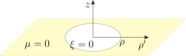
| (22) | |||||
The Laplace equation can then be rewritten Spencer Domina Eberle (1988):
| (23) |
The boundary conditions in this coordinates will be for ( and ) and for the region (, )
One can check by direct substitution that the solution at of the equation with these boundary conditions is:
| (24) |
Thus in the contact between two spheres (, ):
| (25) |
III.2 The energy of the intermediate state
Here we study a cubic lattice of touching NCs with the period . For large it can be considered as the lattice of identical capacitors with capacitance connecting nearest neighbor sites. One can immediately get that the macroscopic dielectric constant of the NC array is . We calculate the energy for the intermediate state, where an electron and a hole occupy the nearest-neighbor NC, the reference point of energy being energy of all neutral NCs. The Coulomb energy necessary to add one electron (or hole) to a neutral NC is called the charging energy . It was shown Reich and Shklovskii (2016) that for touching NCs which are arranged in the cubic lattice this energy is:
| (26) |
We show here that the interaction energy between two nearest neighbors NC is , so that the energy of the intermediate state is , where . Let us first remind the derivation of the result (26).
By the definition the charging energy is
| (27) |
where is the capacitance of a NC immersed in the array. It is known that the capacitance between a site in the cubic lattice made of identical capacitance and the infinity is , Zhang and Shklovskii (2004); Guttmann (2010). We see that plays the role of the effective number of parallel capacitors connecting this site to infinity. Thus we arrive at
| (28) |
Here we also need the interaction energy between two oppositely charged nearest sites of the cubic lattice.
| (29) |
where is the total capacitance between the two nearest-neighbor NCs. It is easy to get that , so that
| (30) |
Thus we arrive at the energy of the intermediate state for the cubic lattice: , i.e. for this case we get . We repeated this derivation for other lattices. We arrived at and for bcc and fcc latices of capacitors, respectively.
III.3 Calculation of
One can calculate the integral (15) in the following way. in the left NC can be written as . We start from the second Green identity for functions and :
| (31) |
Because satisfies the Eq. (19) and is zero on the surface of a NC except the contact facet, where it is equal to we get:
III.4 Non-parabolic band approximation
Below we use non-parabolic “relativistic” Kane approach Wang et al. (1987). Namely we assume that the wave function of an electron and hole in the ground state of the isolated spherical NC satisfies Klein-Gordon equation:
| (32) |
This approximation works well for the ground state of an electron and hole Wang et al. (1987). The energy spectrum is:
| (33) |
One can immediately see that the bulk band gap . The solution of the equation (32) for spherical isolated NC is the same as in the parabolic band approximation (see Eq. (8)). The kinetic energy becomes:
| (34) |
Let us now concetrate on the expression for . If two NCs are separated their 1S ground state is degenerate. When they touch each other by small facet with radius , the degeneracy is lifted and the 1S state is split into two levels and corresponding to the electron wave functions:
| (35) |
which are symmetric and antisymmetric about the plane . The difference between two energies , where is the overlap integral between NCs. Similarly to the problem 3 in 50 of Ref. Landau and Lifshits (1977) we use that satisfies the Eq. (32) with the energy and satisfies the same equation with the energy . As a result we get the difference:
| (36) |
Repeating the same step for we arrive at:
| (37) |
One can check that this expression at leads to (10). For we get:
| (38) |
Using the same approach for the calculation of the integral as in S1 we get:
| (39) |
In that case the Eq. (6) for the ratio tandem and Förster rates can be written as:
| (40) |
and the ratio between tandem and Dexter rates is:
| (41) |
IV Acknowledgement
We are grateful to A. V. Chubukov, P. Crowell, Al. L. Efros, H. Fu, R. Holmes, A. Kamenev, U. R. Kortshagen, A. V. Rodina, I. Rousochatzakis, M. Sammon, B. Skinner, M.V. Voloshin, D. R. Yakovlev and I. N. Yassievich for helpful discussions. This work was supported primarily by the National Science Foundation through the University of Minnesota MRSEC under Award No. DMR-1420013.
References
- Shirasaki et al. (2012) Shirasaki, Y.; Supran, G. J.; Bawendi, M. G.; Bulovic, V. Emergence of Colloidal Quantum-Dot Light-Emitting Technologies. Nat. Photonics 2012, 7, 13–23.
- Liu et al. (2009) Liu, C.-Y.; Holman, Z. C.; Kortshagen, U. R. Hybrid Solar Cells from P3HT and Silicon Nanocrystals. Nano Lett. 2009, 9, 449–452.
- Gur et al. (2005) Gur, I.; Fromer, N. A.; Geier, M. L.; Alivisatos, A. P. Air-Stable All-Inorganic Nanocrystal Solar Cells Processed from Solution. Science 2005, 310, 462–465.
- Yang et al. (2015) Yang, Y.; Zheng, Y.; Cao, W.; Titov, A.; Hyvonen, J.; Manders, J. R.; Xue, J.; Holloway, P. H.; Qian, L. High-Efficiency Light-Emitting Devices Based on Quantum Dots with Tailored Nanostructures. Nat. Photonics 2015, 9, 259-266.
- Gong et al. (2016) Gong, X.; Yang, Z.; Walters, G.; Comin, R.; Ning, Z.; Beauregard, E.; Adinolfi, V.; Voznyy, O.; Sargent, E. H. Highly Efficient Quantum Dot Near-Infrared Light-Emitting Diodes. Nat. Photonics 2016, 10, 253–257.
- Bae et al. (2013) Bae, W. K.; Park, Y.-S.; Lim, J.; Lee, D.; Padilha, L. A.; McDaniel, H.; Robel, I.; Lee, C.; Pietryga, J. M.; Klimov, V. I. Controlling the Influence of Auger Recombination on the Performance of Quantum-Dot Light-Emitting Diodes. Nat. Commun. 2013, 4, 2661.
- Straus et al. (2015) Straus, D. B.; Goodwin, E. D.; Gaulding, E. A.; Muramoto, S.; Murray, C. B.; Kagan, C. R. Increased Carrier Mobility and Lifetime in CdSe Quantum Dot Thin Films through Surface Trap Passivation and Doping. J. Phys. Chem. Lett. 2015, 6, 4605–4609.
- Choi et al. (2012) Choi, J.-H.; Fafarman, A. T.; Oh, S. J.; Ko, D.-K.; Kim, D. K.; Diroll, B. T.; Muramoto, S.; Gillen, J. G.; Murray, C. B.; Kagan, C. R. Bandlike Transport in Strongly Coupled and Doped Quantum Dot Solids: A Route to High-Performance Thin-Film Electronics. Nano Lett. 2012, 12, 2631–2638.
- Reich et al. (2014) Reich, K. V.; Chen, T.; Shklovskii, B. I. Theory of a Field-Effect Transistor Based on a Semiconductor Nanocrystal Array. Phys. Rev. B 2014, 89, 235303.
- Liu et al. (2013) Liu, Y.; Tolentino, J.; Gibbs, M.; Ihly, R.; Perkins, C. L.; Liu, Y.; Crawford, N.; Hemminger, J. C.; Law, M. PbSe Quantum Dot Field-Effect Transistors with Air-Stable Electron Mobilities above . Nano Lett. 2013, 13, 1578–1567.
- Choi et al. (2016) Choi, J.-H.; Wang, H.; Oh, S. J.; Paik, T.; Sung, P.; Sung, J.; Ye, X.; Zhao, T.; Diroll, B. T.; Murray, C. B.; Kagan, C. R. Exploiting the Colloidal Nanocrystal Library to Construct Electronic Devices. Science 2016, 352, 205–208.
- Keuleyan et al. (2011) Keuleyan, S.; Lhuillier, E.; Brajuskovic, V.; Guyot-Sionnest, P. Mid-Infrared HgTe Colloidal Quantum Dot Photodetectors. Nat. Photonics 2011, 5, 489–493.
- Jeong and Guyot-Sionnest (2016) Jeong, K. S.; Guyot-Sionnest, P. Mid-Infrared Photoluminescence of CdS and CdSe Colloidal Quantum Dots. ACS Nano 2016, 10, 2225–2231.
- Talapin et al. (2010) Talapin, D. V.; Lee, J.-S.; Kovalenko, M. V.; Shevchenko, E. V. Prospects of Colloidal Nanocrystals for Electronic and Optoelectronic Applications. Chem. Rev. (Washington, DC, U. S.) 2010, 110, 389–458.
- Kagan and Murray (2015) Kagan, C. R.; Murray, C. B. Charge Transport in Strongly Coupled Quantum Dot Solids. Nat. Nanotechnol. 2015, 10, 1013–1026.
- Liu et al. (2013) Liu, W.; Lee, J.-S.; Talapin, D. V. III-V Nanocrystals Capped with Molecular Metal Chalcogenide Ligands: High Electron Mobility and Ambipolar Photoresponse. J. Am. Chem. Soc. 2013, 135, 1349–1357.
- Lanigan and Thimsen (2016) Lanigan, D.; Thimsen, E. Contact Radius and the Insulator–Metal Transition in Films Comprised of Touching Semiconductor Nanocrystals. ACS Nano 2016, 10, 6744–6752.
- Oh et al. (2014) Oh, S. J.; Berry, N. E.; Choi, J.-H.; Gaulding, E. A.; Lin, H.; Paik, T.; Diroll, B. T.; Muramoto, S.; Murray, C. B.; Kagan, C. R. Designing High-Performance PbS and PbSe Nanocrystal Electronic Devices through Stepwise, Post-Synthesis, Colloidal Atomic Layer Deposition. Nano Letters 2014, 14, 1559–1566.
- Delerue (2016) Delerue, C. Nanocrystal Solids: Order and Progress. Nat. Mater. 2016, 15, 498–499.
- Williams et al. (2009) Williams, K. J.; Tisdale, W. A.; Leschkies, K. S.; Haugstad, G.; Norris, D. J.; Aydil, E. S.; Zhu, X.-Y. Strong Electronic Coupling in Two-Dimensional Assemblies of Colloidal PbSe Quantum Dots. ACS Nano 2009, 3, 1532–1538.
- Walravens et al. (2016) Walravens, W.; Roo, J. D.; Drijvers, E.; ten Brinck, S.; Solano, E.; Dendooven, J.; Detavernier, C.; Infante, I.; Hens, Z. Chemically Triggered Formation of Two-Dimensional Epitaxial Quantum Dot Superlattices. ACS Nano 2016, 10, 6861–6870.
- Baumgardner et al. (2013) Baumgardner, W. J.; Whitham, K.; Hanrath, T. Confined-but-Connected Quantum Solids via Controlled Ligand Displacement. Nano Lett. 2013, 13, 3225–3231.
- Sandeep et al. (2014) Sandeep, C. S. S.; Azpiroz, J. M.; Evers, W. H.; Boehme, S. C.; Moreels, I.; Kinge, S.; Siebbeles, L. D. A.; Infante, I.; Houtepen, A. J. Epitaxially Connected PbSe Quantum-Dot Films: Controlled Neck Formation and Optoelectronic Properties. ACS Nano 2014, 8, 11499–11511.
- Li et al. (2016) Li, H.; Zhitomirsky, D.; Dave, S.; Grossman, J. C. Toward the Ultimate Limit of Connectivity in Quantum Dots with High Mobility and Clean Gaps. ACS Nano 2016, 10, 606–614.
- Whitham et al. (2016) Whitham, K.; Yang, J.; Savitzky, B. H.; Kourkoutis, L. F.; Wise, F.; Hanrath, T. Charge Transport And Localization In Atomically Coherent Quantum Dot Solids. Nat. Mater. 2016, 15, 557–563.
- Evers et al. (2015) Evers, W. H.; Schins, J. M.; Aerts, M.; Kulkarni, A.; Capiod, P.; Berthe, M.; Grandidier, B.; Delerue, C.; van der Zant, H. S. J.; van Overbeek, C.; Peters, J. L. ;Vanmaekelbergh, D.; Siebbeles L. D. A. High Charge Mobility in Two-Dimensional Percolative Networks of PbSe Quantum Dots Connected by Atomic Bonds. Nat. Commun. 2015, 6, 8195.
- Jang et al. (2015) Jang, J.; Dolzhnikov, D. S.; Liu, W.; Nam, S.; Shim, M.; Talapin, D. V. Solution-Processed Transistors Using Colloidal Nanocrystals with Composition-Matched Molecular “Solders”: Approaching Single Crystal Mobility. Nano Lett. 2015, 15, 6309–6317.
- Fu et al. (2016) Fu, H.; Reich, K. V.; Shklovskii, B. I. Hopping Conductivity and Insulator-Metal Transition in Films of Touching Semiconductor Nanocrystals. Phys. Rev. B 2016, 93, 125430.
- Chen et al. (2016) Chen, T.; Reich, K. V.; Kramer, N. J.; Fu, H.; Kortshagen, U. R.; Shklovskii, B. I. Metal-Insulator Transition in Films of Doped Semiconductor Nanocrystals. Nat. Mater. 2016,
- Kagan et al. (1996) Kagan, C. R.; Murray, C. B.; Bawendi, M. G. Long-Range Resonance Transfer of Electronic Excitations in Close-Packed CdSe Quantum-Dot Solids. Phys. Rev. B 1996, 54, 8633–8643.
- Crooker et al. (2002) Crooker, S. A.; Hollingsworth, J. A.; Tretiak, S.; Klimov, V. I. Spectrally Resolved Dynamics of Energy Transfer in Quantum-Dot Assemblies: Towards Engineered Energy Flows in Artificial Materials. Phys. Rev. Lett. 2002, 89, 186802.
- Miyazaki and Kinoshita (2012) Miyazaki, J.; Kinoshita, S. Site-Selective Spectroscopic Study on the Dynamics of Exciton Hopping in an Array of Inhomogeneously Broadened Quantum Dots. Phys. Rev. B 2012, 86, 035303.
- Achermann et al. (2003) Achermann, M.; Petruska, M. A.; Crooker, S. A.; Klimov, V. I. Picosecond Energy Transfer in Quantum Dot Langmuir−Blodgett Nanoassemblies. J. Phys. Chem. B 2003, 107, 13782–13787.
- Kholmicheva et al. (2015) Kholmicheva, N.; Moroz, P.; Bastola, E.; Razgoniaeva, N.; Bocanegra, J.; Shaughnessy, M.; Porach, Z.; Khon, D.; Zamkov, M. Mapping the Exciton Diffusion in Semiconductor Nanocrystal Solids. ACS Nano 2015, 9, 2926–2937.
- Poulikakos et al. (2014) Poulikakos, L. V.; Prins, F.; Tisdale, W. A. Transition from Thermodynamic to Kinetic-Limited Excitonic Energy Migration in Colloidal Quantum Dot Solids. J. Phys. Chem. C 2014, 118, 7894–7900.
- Crisp et al. (2013) Crisp, R. W.; Schrauben, J. N.; Beard, M. C.; Luther, J. M.; Johnson, J. C. Coherent Exciton Delocalization in Strongly Coupled Quantum Dot Arrays. Nano Lett. 2013, 13, 4862–4869.
- Mork et al. (2014) Mork, A. J.; Weidman, M. C.; Prins, F.; Tisdale, W. A. Magnitude of the Förster Radius in Colloidal Quantum Dot Solids. J. Phys. Chem. C 2014, 118, 13920–13928.
- Akselrod et al. (2014) Akselrod, G. M.; Prins, F.; Poulikakos, L. V.; Lee, E. M. Y.; Weidman, M. C.; Mork, A. J.; Willard, A. P.; Bulovic, V.; Tisdale, W. A. Subdiffusive Exciton Transport in Quantum Dot Solids. Nano Lett. 2014, 14, 3556–3562.
- Murray et al. (2000) Murray, C. B.; Kagan, C. R.; Bawendi, M. G. Synthesis And Characterization Of Monodisperse Nanocrystals And Close-Packed Nanocrystal Assemblies. Annu. Rev. Mater. Sci. 2000, 30, 545–610.
- Kalesaki et al. (2014) Kalesaki, E.; Delerue, C.; Morais Smith, C.; Beugeling, W.; Allan, G.; Vanmaekelbergh, D. Dirac Cones, Topological Edge States, and Nontrivial Flat Bands in Two-Dimensional Semiconductors with a Honeycomb Nanogeometry. Phys. Rev. X 2014, 4, 011010.
- Kalesaki et al. (2013) Kalesaki, E.; Evers, W. H.; Allan, G.; Vanmaekelbergh, D.; Delerue, C. Electronic Structure of Atomically Coherent Square Semiconductor Superlattices with Dimensionality Below Two. Phys. Rev. B 2013, 88, 115431.
- Beugeling et al. (2015) Beugeling, W.; Kalesaki, E.; Delerue, C.; Niquet, Y.-M.; Vanmaekelbergh, D.; Smith, C. M. Topological States in Multi-Orbital HgTe Honeycomb Lattices. Nat. Commun. 2015, 6, 6316.
- Madelung (2013) Madelung, O. Semiconductors: Data Handbook; Springer:New-York, 2004 .
- Reich and Shklovskii (2016) Reich, K. V.; Shklovskii, B. I. Dielectric Constant and Charging Energy in Array of Touching Nanocrystals. Appl. Phys. Lett. 2016, 108, 113104.
- Nirmal et al. (1995) Nirmal, M.; Norris, D. J.; Kuno, M.; Bawendi, M. G.; Efros, A. L.; Rosen, M. Observation of the ”Dark Exciton” in CdSe Quantum Dots. Phys. Rev. Lett. 1995, 75, 3728–3731.
- Dexter (1953) Dexter, D. L. A Theory of Sensitized Luminescence in Solids. J. Chem. Phys. 1953, 21, 836–850.
- Liu et al. (2015) Liu, F.; Rodina, A. V.; Yakovlev, D. R.; Golovatenko, A. A.; Greilich, A.; Vakhtin, E. D.; Susha, A.; Rogach, A. L.; Kusrayev, Y. G.; Bayer, M. Förster Energy Transfer of Dark Excitons Enhanced by a Magnetic Field in an Ensemble of CdTe Colloidal Nanocrystals. Phys. Rev. B 2015, 92, 125403.
- Blumling et al. (2012) Blumling, D. E.; Tokumoto, T.; McGill, S.; Knappenberger, K. L. Temperature- and Field-Dependent Energy Transfer in CdSe Nanocrystal Aggregates Studied by Magneto-Photoluminescence Spectroscopy. Phys. Chem. Chem. Phys. 2012, 14, 11053.
- Landau and Lifshits (1977) Landau, L.; Lifshits, E. Quantum Mechanics: Non-relativistic Theory; Butterworth Heinemann: New-York, 1977.
- Moskalenko and Yassievich (2004) Moskalenko, A. S.; Yassievich, I. N. Excitons in Si Nanocrystals. Phys. Solid State 2004, 46, 1508–1519.
- Burdov (2002) Burdov, V. A. Electron and Hole Spectra of Silicon Quantum Dots. J. Exp. Theor. Phys. 2002, 94, 411–418.
- Allan and Delerue (2007) Allan, G.; Delerue, C. Energy Transfer Between Semiconductor Nanocrystals: Validity of Förster’s Theory. Phys. Rev. B 2007, 75.
- Poddubny and Rodina (2016) Poddubny, A. N.; Rodina, A. V. Nonradiative and Radiative Förster Energy Transfer Between Quantum Dots. J. Exp. Theor. Phys. 2016, 122, 531–538.
- Blood (2015) Blood, P. Quantum Confined Laser Devices: Optical gain and recombination in semiconductors; Oxford University Press: Oxford, 2015.
- Efros and Rosen (2000) Efros, A. L.; Rosen, M. The Electronic Structure of Semiconductor Nanocrystals. Annu. Rev. Mater. Sci. 2000, 30, 475–521.
- Anderson (1963) Anderson, P. W. In Solid State Physics; Seitz, F., Turnbull, D., Eds.; Academic Press: New-York, 1963; Vol. 14; pp 99 – 214.
- Kang and Wise (1997) Kang, I.; Wise, F. W. Electronic Structure and Optical Properties of PbS and PbSe Quantum Dots. J. Opt. Soc. Am. B 1997, 14, 1632–1646.
- Wang et al. (1987) Wang, Y.; Suna, A.; Mahler, W.; Kasowski, R. PbS in Polymers. From Molecules to Bulk Solids. J. Chem. Phys. 1987, 87, 7315–7322.
- Allan and Delerue (2004) Allan, G.; Delerue, C. Confinement Effects in PbSe Quantum Wells and Nanocrystals. Phys. Rev. B 2004, 70.
- Rayleigh (1897) Rayleigh, F. R. S. On the Passage of Waves Through Apertures in Plane Screens, and Allied Problems. Philos. Mag. (1798-1977) 1897, 43, 259–272.
- Spencer Domina Eberle (1988) Moon, P.; Spencer, D.E. Field Theory Handbook: Including Coordinate Systems- Differential Equations- and Their Solutions; A Springer-Verlag Telos: New-York, 1988.
- Zhang and Shklovskii (2004) Zhang, J.; Shklovskii, B. I. Density of States and Conductivity of a Granular Metal or an Array of Quantum Dots. Phys. Rev. B 2004, 70, 115317.
- Guttmann (2010) Guttmann, A. J. Lattice Green’s Functions in All Dimensions. J. Phys. A: Math. Theor. 2010, 43, 305205.