Graphene Transport Mediated by Micropatterned Substrates
Abstract
Engineered substrates offer a promising avenue towards graphene devices having tunable properties. In particular, topographically patterned substrates can expose unique behavior due to their ability to induce local variations in strain and electrostatic doping. However, to explore the range of possible science and applications, it is important to create topographic substrates which both have tunable features and are suitable for transport measurements. In this Letter we describe the fabrication of tunable, topographically patterned substrates suitable for transport measurements. We report both optical and transport measurements of graphene devices fabricated on these substrates, and demonstrate characteristic strain and local doping behavior induced by the topographic features.
Graphene is a material with enormous potential for both scientific research and technical applications Novoselov et al. (2004, 2005); Zhang et al. (2005); Geim and Novoselov (2007). In particular, the ability to tune graphene’s properties through the use of engineered substrates offers a practical method to explore graphene’s properties and modify them for specific applicationsGuinea, Katsnelson, and Geim (2010); Zhou et al. (2007). Previous work on engineered substrates has employed substrate topographyTomori et al. (2011); Mi et al. (2015); Babichev et al. (2015); Reserbat-Plantey et al. (2014), electrostatic charge injectionChiu et al. (2010), substrate lattice mis-matchZhou et al. (2007), and ferroelectric polarizationHinnefeld et al. (2016) to achieve a range of modifications to graphene’s properties.


Of the various substrate engineering techniques, topographic substrate patterning has two distinct advantages: first, topographic substrates can create local strain in graphene. Strain has large effects on graphene’s electrical properties Pereira and Castro Neto (2009), from inducing minigaps Ni et al. (2008) to creating large pseudo-magnetic fields Guinea, Katsnelson, and Geim (2010); Levy et al. (2010). To date however the techniques used to produce strain in graphene are either not amenable to performing electrical transport measurements on graphene Levy et al. (2010); Tomori et al. (2011); Mohiuddin et al. (2009); Ni et al. (2008); Gill et al. (2015); Reserbat-Plantey et al. (2014) or not compatible with standard lithographic fabrication procedures Babichev et al. (2015). Second, topographic substrates can modulate the effect of a single electrostatic gate to produce complex doping profiles in graphene without the need for multiple, distinct gate electrodes. Here we demonstrate a fabrication procedure for producing engineered arrays of topographic features on standard silicon substrates, and we report optical measurements of strain and transport measurements of local doping in graphene devices fabricated atop these substrates.

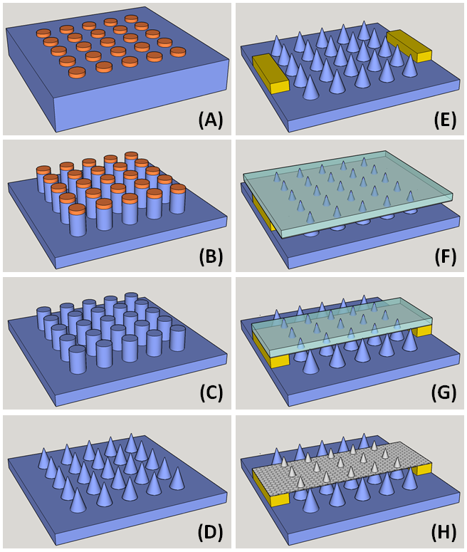
The process used to create the topographic features on the substrate is illustrated schematically in Figures 1A-D. First an array of 20 nm thick copper circles is deposited, using standard electron-beam lithography and evaporation techniques, on a silicon chip covered with a 1000 nm layer of thermal oxide. The deposited copper is then used as a mask in a CF4 reactive ion etching (RIE) step to produce cylindrical pillars in the SiO2 layer. The RIE etch time and the diameter of the deposited copper mask circles together define the aspect ratio of the resulting pillars. For these devices we use a mask diameter of 100 nm, and a 10 minute etch time, which gives a height of approximately 200 nm. Pillar diameter is independent of RIE etch time and is equal to the mask diameter. After the etch, the copper mask is removed by immersing the chip in a 0.1M solution of ammonium persulfate for several hours. Finally, the chip is dipped in buffered oxide etchant to sharpen the SiO2 pillars produced during the RIE step into pointed, conical shapes having tips of 20 nm diameter.
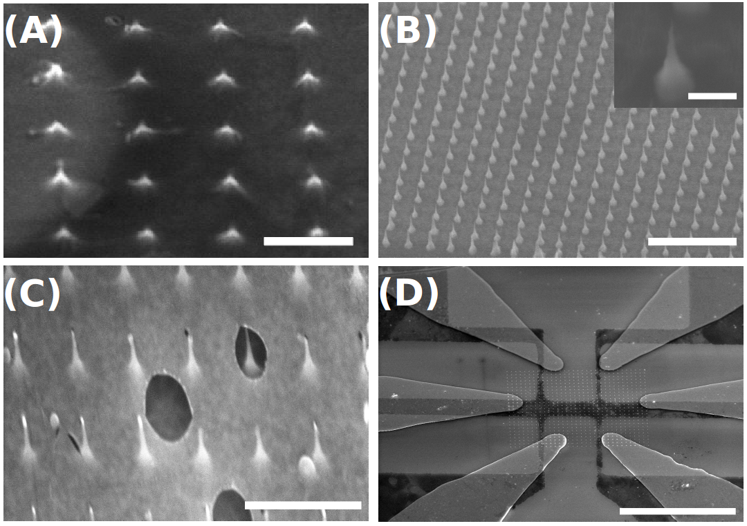
Graphene devices are fabricated on substrates prepared by this method using the process shown in Figures 1E-F. First Ti/Au (5 nm/30 nm) leads and contact pads are defined and deposited using electron-beam lithography and evaporation. Next, a monolayer of graphene is grown on a different substrate using established chemical vapor deposition techniquesLi et al. (2009a). The graphene is then transferred to the topographic substrate using standard polymer-assisted wet-transfer techniquesLi et al. (2009b). The same polymer layer used to transfer the graphene is then used as a resist in an electron-beam lithography step. Next the exposed graphene is removed using a reactive ion etch, yielding graphene in a Hall bar configuration. Finally the remaining polymer resist is dissolved in acetone and the chip is dried in a critical point drying apparatus. Figure 2 shows scanning electron microscope (SEM) micrographs of substrates and graphene devices produced by this process. Although the transfer and drying process does lead to some ripping of the graphene (see holes evident in Figure 2C) holes and rips cover less than 10% of the surface, leaving the graphene largely robust for transport measurements on the 10 - 50 micron length scale of typical devices. As shown in Figure 2A, we do not observe significant ripple formation Babichev et al. (2015); Reserbat-Plantey et al. (2014), likely because our topographic features are widely spaced Yamamoto et al. (2012).
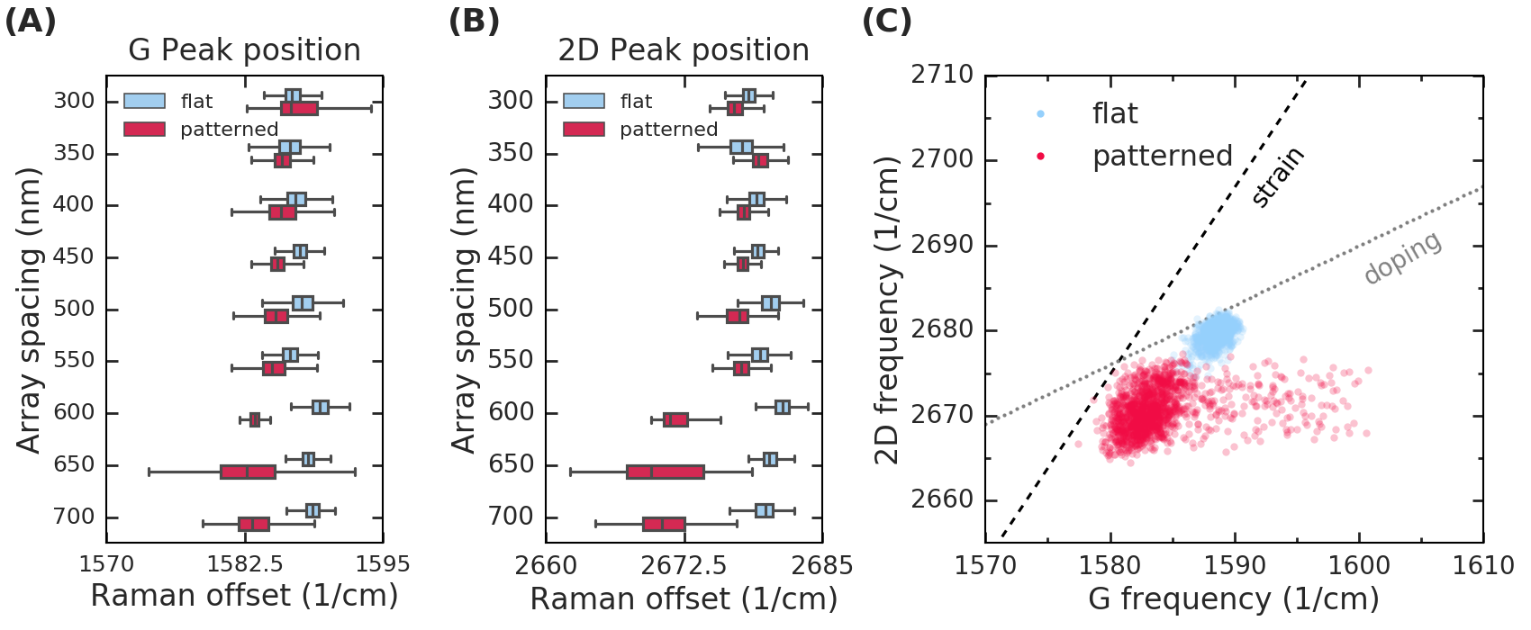
We perform optical measurements of graphene devices fabricated on these substrates to confirm the presence of strain. Raman spectroscopy iss performed using a Nanophoton Raman 11 microscope with a 532 nm laser at room temperature. The laser power iss kept below 1 mW to minimize local heating. Raman measurements are collected in a raster pattern across a 20 m 20 m area with a measurement spot size of 350 nm; each scan encompasses a varying number of topographic features depending on the array spacing. Random variations in spectra for regions away from topographic features yield shifts of less than 0.5 cm-1. The data for the flat substrates is collected separately for each device to account for the varying residual doping present in each sample. At each raster point the Raman G and 2D peak positions are extractedFerrari et al. (2006). Figures 3A and 3B summarize the extracted positions of the Raman G and 2D peaks, respectively, for graphene on topographically patterned and flat regions of devices prepared by the method described above. Data is shown for devices having pillar spacings between 300 and 700 nm.

Both the G and 2D peaks of graphene on the patterned substrate regions display shifted peak positions relative to graphene on the flat regions. This shift increases with increasing topographic feature spacing and displays a qualitative jump for spacings above 600 nm. We attribute this jump to a snap-through transitionGill et al. (2015); Scharfenberg et al. (2012) in the adhesion of the graphene to the substrate: for spacings below 600 nm the graphene is suspended in the entire topographically patterned region, while for spacings above 600 nm the graphene adheres to the substrate except in the immediate vicinity of a topographic feature. The partial delamination present in the sparse topographic samples produces strain in the graphene which generates the shifted Raman peak positions Gill et al. (2015).
Doping from charge impurities in the substrate is also known to shift Raman peak positions in grapheneReina et al. (2008); Casiraghi et al. (2007), however the ratio
| (1) |
(where is the shift in a Raman peak position relative to its intrinsic value) differs between the two mechanisms Lee et al. (2012). Experimental measurements Zabel et al. (2012); Metzger et al. (2009); Ding et al. (2010) and theoretical resultsMohr, Maultzsch, and Thomsen (2010); Mohiuddin et al. (2009) place the ratio for strain between 2.25 and 2.8 and the ratio for doping at approximately 0.75 Lee et al. (2012). Figure 3C shows the extracted Raman G and 2D peak positions for a representative topographically patterned sample having a spacing of 700 nm, along with lines corresponding to (dashed) and (dotted). The difference between the topographic and flat graphene samples lies along ; thus, we attribute the shifted peak positions to the effect of strain in the graphene.
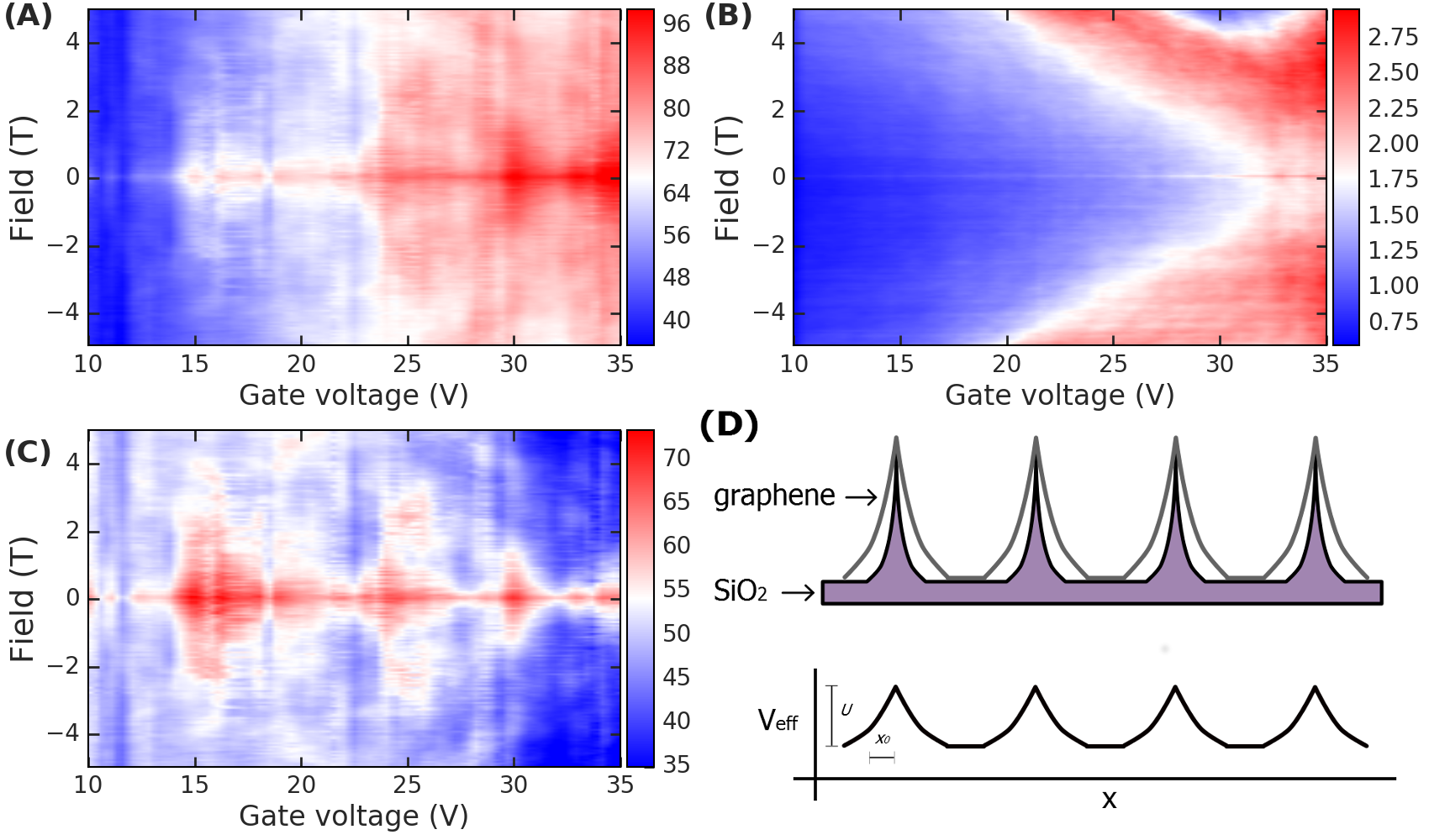
Next we perform magneto-transport measurements on a device having a substrate pillar spacing of 750 nm, to elucidate the effect of local variations in the electrostatic potential. Several similar devices were measured and yielded qualitatively similar results. For sparsely patterned substrates the graphene is locally delaminated in the vicinity of each individual topographic feature. This delamination alters the effective gate capacitance by including a region of vacuum in series with the SiO2 dielectric layer. The local variation in the gate capacitance creates a corresponding variation in the potential, effectively creating a circular potential barrier, e.g. a quantum dot. This situation is illustrated schematically in Figure 4D. Carriers in graphene cannot be confined electrostatically: as massless particles governed by the Dirac equation (in the low energy limit) they display Klein tunneling Katsnelson, Novoselov, and Geim (2006); Young and Kim (2009). However, previous work has shown that circular potential barriers can create pseudo-bound states in graphene Silvestrov and Efetov (2007); Matulis and Peeters (2008); Hewageegana and Apalkov (2008); Chen, Apalkov, and Chakraborty (2007); Heinisch, Bronold, and Fehske (2013). For graphene on topographically patterned substrates we therefore expect transport behavior to display signatures of scattering from these pseudo-bound states. We note that we do not expect coherent transport behavior (such as Fabry-Pérot resonance or superlattice effects) across multiple topographic features, as the coherence length is 1 micron Berger et al. (2006)), and a typical device length is 20 m which encompasses 30 pillars.
Figures 4A and 4B show the results of magneto-transport measurements performed at 250 mK on a 750 nm-spaced topographic device and a flat control device, respectively. Both devices are 20 m long and 10 m wide; for the topographic device the patterned substrate features cover the entire device area. The Dirac point for both devices is located at approximately 40 V; this reflects both the residual doping from the fabrication process as well as the reduced gate capacitance of the thicker-than-normal SiO2 dielectric layer. All transport measurements were taken with a channel current of 50 nA, and gate leakage current was always less than five percent of channel current. The reduced mobility of the topographic device relative to the flat control device is due to rips introduced during the critical point drying step of the fabrication process. Qualitative differences between the topographic and flat devices are apparent: the flat control device displays the onset of a typical Landau level fan patternBolotin et al. (2009), however the topographic device displays several resistance maxima not present in the control device. Figure 4C shows the same data as Figure 4A with a linear background subtracted; we remove this background to emphasize deviations from the expected Dirac cone pattern of gated graphene. Several additional local maxima are visible in the low gate voltage region. The diamond-like high resistance features (red regions in Figure 4C) are reproducible. Although they are somewhat irregular, they have typical energy scales of 1 T in magnetic field, and 5 V in gate voltage.
The scale of the observed transport features, in both magnetic field and gate voltage, is in good agreement with theoretical predictions for scattering from quasi-bound states in graphene. Considering first the magnetic field scale, previous workHeinisch, Bronold, and Fehske (2013) has shown that the scattering properties of quantum dots in graphene depend on the size of the dot: for small dots forward scattering is strongly suppressed and conductivity is reduced, while large dots can focus carriers and enhance conductivity. In the presence of a magnetic field, we take the cyclotron radius to be the relevant length scale, e.g. for dot size we expect an effective “small” dot with reduced conductance, while for we expect a “large” dot with larger conductance. This is consistent with our observation of more resistive behaviour at smaller magnetic fields, i.e. at larger . This can be estimated quantitatively by calculating the cyclotron radius, given by
| (2) |
where m s-1 is the Fermi velocity in graphene, is the carrier effective mass, is the charge of an electron, is the applied magnetic field, is the reduced Planck’s constant, and is the carrier density. For our devices, with a field of 1 T corresponding to the the field at which the transport features disappear and a carrier density of cm-2 as determined by separate Hall measurements, we find a cyclotron radius of 40 nm. This is in excellent agreement with the 50 nm radius of the local delamination regions, as determined by SEM measurements.
Next we consider the gate voltage scale of the transport features. Forward scattering off quasi-bound states in graphene quantum dots is also suppressed when the energy of incident carriers matches the energy of a quasi-bound stateSilvestrov and Efetov (2007). We therefore expect the gate voltage scale of the transport features to match the spacing between quasi-bound state energy levels. Features in the transport data are spaced approximately 5V apart. The change in the Fermi energy in graphene for a given change in gate voltage is given by
| (3) |
where is the capacitive lever arm of the back-gate, the capacitance of the backgate is that of a SiO2 parallel plate capacitor with an area of 200 m2 and a separation of 500 nm, and the quantum capacitance of the graphene sheet is given by Fang et al. (2007) (in the low temperature limit where ). The density of states is known for grapheneCastro Neto et al. (2009), and can be extracted from the carrier density. Using a carrier density of cm-2 as above this gives an energy scale for the observed transport features of approximately 40 meV. Next we relate this experimental value to theoretical predictions.
For a parabolic potential of the form theoretical results Silvestrov and Efetov (2007) give the following expression for the energy scale of the quasi-bound states:
| (4) |
As shown in Figure 4D, the potential profile in our devices is defined by the local delamination of graphene in the vicinity of the topographic features. Approximating the potential profile in our devices as parabolic we take nm to be half the radius of the topographic features, and to be the change in potential created by the locally varying gate capacitance:
| (5) |
The capacitive lever arm for the flat region remains the same as above, and we model the capacitance of the delaminated region as cylinder of air in series with the SiO2 substrate. The cylinder of air has radius and height 100 nm, where the latter figure is half the height of the patterned features on the substrate. Taking as the midpoint of the region of interest we find a theoretically predicted energy scale of 57 meV for the quasi-bound states in our device, in good agreement with our experimental results.
We note that the energy scale of the quasi-bound states depends on the height of the potential barrier as . In our experimental configuration the height of the potential barrier depends in turn on the magnitude of the applied gate voltage as . The gate voltage in our measurements varies by a factor of two in the region of interest, and so we expect the theoretically predicted energy scale to vary by a factor of over the course of the measurement, which precludes a more precise quantitative comparison. It is also possible that local strain and pseudomagnetic fields affect transport in this regime. However, our data is consistent with dots having diameters commensurate with the delamination region, rather than localized around the pillars, which implies that delamination may dominate the physics we observe.
In summary, we describe a fabrication procedure for producing graphene devices on substrates having an array of topographic features and we report experimental signatures caused by these features. We find that the spacing of the topographic features determines the adhesion behavior of the graphene; for large spacings partial delamination creates strain in the graphene which we observe using optical measurements. Finally, we find that magneto-transport measurements display features consistent with the presence of a locally varying potential, which we attribute to the variable gate capacitance induced by the local graphene delamination. These transport features are consistent with the presence of quasi-bound states in the graphene; the tunable nature of the graphene delamination offers an opportunity to deliberately engineer the properties of these quasi-bound states. With careful considerations of the topographic feature spacing and height this technique can be adapted to length scales on the order of the coherence length in graphene, thereby offering a novel method to explore correlated strain and electrostatic potentials along with superlattice effects in graphene.
REFERENCES
References
- Novoselov et al. (2004) K. S. Novoselov, A. K. Geim, S. V. Morozov, D. Jiang, Y. Zhang, S. V. Dubonos, I. V. Grigorieva, and A. A. Firsov, Science 306, 666 (2004).
- Novoselov et al. (2005) K. S. Novoselov, A. K. Geim, S. V. Morozov, D. Jiang, M. Katsnelson, I. V. Grigorieva, S. Dubonos, and A. Firsov, Nature 438, 197 (2005).
- Zhang et al. (2005) Y. Zhang, Y.-W. Tan, H. L. Stormer, and P. Kim, Nature 438, 201 (2005).
- Geim and Novoselov (2007) A. K. Geim and K. S. Novoselov, Nature Materials 6, 183 (2007).
- Guinea, Katsnelson, and Geim (2010) F. Guinea, M. I. Katsnelson, and A. K. Geim, Nature Physics 6, 30 (2010).
- Zhou et al. (2007) S. Y. Zhou, G.-H. Gweon, A. V. Fedorov, P. N. First, W. A. De Heer, D.-H. Lee, F. Guinea, A. H. Castro Neto, and A. Lanzara, Nature Materials 6, 770 (2007).
- Tomori et al. (2011) H. Tomori, A. Kanda, H. Goto, Y. Ootuka, K. Tsukagoshi, S. Moriyama, E. Watanabe, and D. Tsuya, Applied Physics Express 4, 075102 (2011).
- Mi et al. (2015) H. Mi, S. Mikael, C.-C. Liu, J.-H. Seo, G. Gui, A. L. Ma, P. F. Nealey, and Z. Ma, Applied Physics Letters 107, 143107 (2015).
- Babichev et al. (2015) A. V. Babichev, S. A. Rykov, M. Tchernycheva, A. N. Smirnov, V. Y. Davydov, Y. A. Kumzerov, and V. Y. Butko, ACS applied materials & interfaces 8, 240 (2015).
- Reserbat-Plantey et al. (2014) A. Reserbat-Plantey, D. Kalita, Z. Han, L. Ferlazzo, S. Autier-Laurent, K. Komatsu, C. Li, R. Weil, A. Ralko, L. Marty, et al., Nano letters 14, 5044 (2014).
- Chiu et al. (2010) H.-Y. Chiu, V. Perebeinos, Y.-M. Lin, and P. Avouris, Nano Letters 10, 4634 (2010).
- Hinnefeld et al. (2016) J. H. Hinnefeld, R. Xu, S. Rogers, S. Pandya, M. Shim, L. W. Martin, and N. Mason, Applied Physics Letters 108, 203109 (2016).
- Pereira and Castro Neto (2009) V. M. Pereira and A. H. Castro Neto, Physical Review Letters 103, 046801 (2009).
- Ni et al. (2008) Z. H. Ni, T. Yu, Y. H. Lu, Y. Y. Wang, Y. P. Feng, and Z. X. Shen, ACS Nano 2, 2301 (2008).
- Levy et al. (2010) N. Levy, S. A. Burke, K. L. Meaker, M. Panlasigui, A. Zettl, F. Guinea, A. H. Castro Neto, and M. F. Crommie, Science 329, 544 (2010).
- Mohiuddin et al. (2009) T. M. G. Mohiuddin, A. Lombardo, R. R. Nair, A. Bonetti, G. Savini, R. Jalil, N. Bonini, D. M. Basko, C. Galiotis, N. Marzari, et al., Physical Review B 79, 205433 (2009).
- Gill et al. (2015) S. T. Gill, J. H. Hinnefeld, S. Zhu, W. J. Swanson, T. Li, and N. Mason, ACS Nano 9, 5799 (2015).
- Lee et al. (2012) J. E. Lee, G. Ahn, J. Shim, Y. S. Lee, and S. Ryu, Nature Communications 3, 1024 (2012).
- Li et al. (2009a) X. Li, W. Cai, J. An, S. Kim, J. Nah, D. Yang, R. Piner, A. Velamakanni, I. Jung, E. Tutuc, S. K. Banerjee, L. Colombo, and R. S. Ruoff, Science 324, 1312 (2009a).
- Li et al. (2009b) X. Li, Y. Zhu, W. Cai, M. Borysiak, B. Han, D. Chen, R. D. Piner, L. Colombo, and R. S. Ruoff, Nano Letters 9, 4359 (2009b).
- Yamamoto et al. (2012) M. Yamamoto, O. Pierre-Louis, J. Huang, M. S. Fuhrer, T. L. Einstein, and W. G. Cullen, Physical Review X 2, 041018 (2012).
- Ferrari et al. (2006) A. Ferrari, J. Meyer, V. Scardaci, C. Casiraghi, M. Lazzeri, F. Mauri, S. Piscanec, D. Jiang, K. Novoselov, S. Roth, et al., Physical Review Letters 97, 187401 (2006).
- Scharfenberg et al. (2012) S. Scharfenberg, N. Mansukhani, C. Chialvo, R. L. Weaver, and N. Mason, Applied Physics Letters 100, 021910 (2012).
- Reina et al. (2008) A. Reina, X. Jia, J. Ho, D. Nezich, H. Son, V. Bulovic, M. S. Dresselhaus, and J. Kong, Nano Letters 9, 30 (2008).
- Casiraghi et al. (2007) C. Casiraghi, S. Pisana, K. S. Novoselov, A. K. Geim, and A. C. Ferrari, Applied Physics Letters 91, 233108 (2007).
- Zabel et al. (2012) J. Zabel, R. R. Nair, A. Ott, T. Georgiou, A. K. Geim, K. S. Novoselov, and C. Casiraghi, Nano Letters 12, 617 (2012).
- Metzger et al. (2009) C. Metzger, S. Rémi, M. Liu, S. V. Kusminskiy, A. H. Castro Neto, A. K. Swan, and B. B. Goldberg, Nano Letters 10, 6 (2009).
- Ding et al. (2010) F. Ding, H. Ji, Y. Chen, A. Herklotz, K. Dörr, Y. Mei, A. Rastelli, and O. G. Schmidt, Nano Letters 10, 3453 (2010).
- Mohr, Maultzsch, and Thomsen (2010) M. Mohr, J. Maultzsch, and C. Thomsen, Physical Review B 82, 201409 (2010).
- Katsnelson, Novoselov, and Geim (2006) M. Katsnelson, K. S. Novoselov, and A. K. Geim, Nature Physics 2, 620 (2006).
- Young and Kim (2009) A. F. Young and P. Kim, Nature Physics 5, 222 (2009).
- Silvestrov and Efetov (2007) P. G. Silvestrov and K. B. Efetov, Physical Review Letters 98, 016802 (2007).
- Matulis and Peeters (2008) A. Matulis and F. M. Peeters, Physical Review B 77, 115423 (2008).
- Hewageegana and Apalkov (2008) P. Hewageegana and V. Apalkov, Physical Review B 77, 245426 (2008).
- Chen, Apalkov, and Chakraborty (2007) H.-Y. Chen, V. Apalkov, and T. Chakraborty, Physical Review Letters 98, 186803 (2007).
- Heinisch, Bronold, and Fehske (2013) R. L. Heinisch, F. X. Bronold, and H. Fehske, Physical Review B 87, 155409 (2013).
- Berger et al. (2006) C. Berger, Z. Song, X. Li, X. Wu, N. Brown, C. Naud, D. Mayou, T. Li, J. Hass, A. N. Marchenkov, et al., Science 312, 1191 (2006).
- Bolotin et al. (2009) K. I. Bolotin, F. Ghahari, M. D. Shulman, H. L. Stormer, and P. Kim, Nature 462, 196 (2009).
- Fang et al. (2007) T. Fang, A. Konar, H. Xing, and D. Jena, Applied Physics Letters 91, 092109 (2007).
- Castro Neto et al. (2009) A. H. Castro Neto, N. M. R. Peres, K. S. Novoselov, and A. K. Geim, Reviews of Modern Physics 81, 109 (2009).