Sense Amplifier Comparator with Offset Correction for Decision Feedback Equalization based Receivers
A decision feedback circuit with integrated offset compensation is presented in this paper. The circuit is built around the sense amplifier comparator. The feedback loop is closed around the first stage of the comparator resulting in minimum loop latency. The feedback loop is implemented using a switched capacitor network that picks from one of pre-computed voltages to be fed back. The comparator’s offset that is to be compensated for, is added in the same path. Hence, an extra offset correction input is not required. The circuit is used as a receiver for a 10 mm low swing interconnect implemented in UMC 130 nm CMOS technology. The circuit is tested at a frequency of 1 GHz and it consumes 145 A from a 1.2V supply at this frequency.
1 Introduction
Decision-Feedback-equalization (DFE) is a technique that compensates for Inter-Symbol-Interference (ISI) in a serial input digital data signal (?, ?, ?, ?). Fig. 1 shows the block diagram of a DFE circuit. In this technique, a hard decision is made on the input in every clock cycle. This decision is scaled and subtracted from the input before the next sampling event. The scaling factor is chosen based on the amount of previous bit ISI in the input data. If the initial decision is correct, this effectively erases the memory of the previous bit. The delay involved in making the hard decision, scaling it and subtracting from the next input limits the maximum frequency of operation of this circuit. Further, in scaled technologies the decision devices have inherent offset that needs to be compensated for. In this paper, we propose a DFE circuit built around the Sense amplifier comparator that has low loop latency and features integrated offset compensation.
DFE is a simple technique and has found wide applications from low power to high performance communication systems. DFE has been proposed as an effective way of extending the bandwidth of repeaterless low swing interconnects (?, ?). DFE has also been used to correct for errors in digital systems (?), for implementing low power logic circuits based on pass transistor logic (?) and for enhancing bandwidth of flip-flops (?). A sense amplifier comparator (?) is used in most of these circuits as it can achieve high speed at low power consumption. When used for sampling low swing data, these comparators need offset compensation. Previous works have implemented this using an auxiliary input to the core comparator (?, ?). In high speed designs where the loop delay becomes the bottleneck, look-ahead-dfe is used (?, ?). In look-ahead-dfe, multiple comparators make decisions on the input data, each assuming a possible value of the previous decision. This increases the number of comparators needed, each requiring its own offset compensation circuit as well.
In this paper, we propose a DFE circuit that has low latency and integrated offset compensation. The feedback loop is built with a switched capacitor circuit, driven by the first stage of the sense amplifier, which picks from pre-computed inputs for the feedback. The offset to be corrected is added to the same feedback input, removing the need for an extra offset correction input to the comparator. The circuit is designed and fabricated in UMC 130 nm CMOS technology for a data rate of 1GHz. A double differential architecture, with a differential main input and differential feedback input, is used. For testing the equalizer, the comparator is used as a receiver of a 10 mm on-chip interconnect with a capacitively coupled low swing transmitter reported by Mensink et al. in (?).
2 DFE with switched capacitor feedback
In time domain, the output of the DFE circuit can be expressed in terms of the comparator input as
| (1) |
Here, is the hard decision made by the comparator in the previous cycle and is a constant that is less than . is chosen depending on the amount of ISI present in the input data. The difference equation
is a high pass function, which compensates for the ISI produced by the low pass nature of the interconnect. Since is a hard decision, the term can take only one of two values, i.e.
The analysis till now assumes an ideal comparator. Practically, comparators also suffer from offset, which needs to be corrected. To compensate for the inherent offset of the comparator, the offset correction can added within the same feedback i.e.
We implement the DFE circuit using a switched capacitor circuit that uses the comparator output to select from pre-computed voltages that correspond to and for the feedback. Since most of the applications use differential input architecture, a comparator with a double differential input, i.e. with a differential main input and differential feedback input is used. Such an implementation needs two precomputed differential bias inputs with different common modes, for the feedback network to pick from. Hence, a total of 4 distinct bias voltages are needed. This is explained in the following.
When , the differential feedback voltages can be written as
Similarly, ,
Here, is the common mode of the feedback input. This is illustrated graphically in Fig. 2, along with the block diagram of the comparator with a double differential input.
To summarize, the voltages and are the four feedback bias voltages. The difference (= ) corresponds to the feedback factor . The common modes of these two differential pairs are skewed by the offset to be corrected, as illustrated in Fig. 2.
We use the sense amplifier based comparator in the DFE circuit. The circuit diagram of the first stage of the comparator is shown in Fig. 3. An additional input transistor pair is used for the feedback input (?).
The second stage of the comparator is an SR slave latch (?). Prior implementations of DFE using this comparator have used the slave latch output for the decision feedback (?). We use the first stage output itself for the feedback, which results in minimum latency. The nodes and are precharged in every cycle to . During the input evaluation phase, these nodes discharge through the input transistors and depending on the input, one of the nodes discharges faster than the other. When and are discharged below the trip point of the inverters formed by and , the inverter positive feedback pulls and apart in the direction established by the input pair. Typical waveforms of and are shown in Fig. 4.
The output of the first stage is used to drive a switched capacitor network which picks from the two pairs of differential bias voltages for the feedback. This effectively results in a low swing dynamic latch for the decision feedback. The circuit implementation is discussed in the next section.
3 Circuit implementation
In this section we shall discuss the circuit implementation. The first subsection will describe the implementation of the comparator and the second subsection will describe the bias voltage generation. The circuit was designed in UMC 130 nm CMOS technology.
3.1 Comparator with DFE
As discussed in the previous section, we shall use the sense amplifier comparator. The feedback network is a switched capacitor circuit driven by the first stage of the comparator, which is shown in Fig. 5.
In every clock cycle the comparator is reset, i.e. both and are precharged to . This puts the multiplexer in a high impedance state. During input sample evaluation, one of or fall lower than the other, and the output of the analog multiplexer generates the scaled version of the resolved bit. This output is held dynamically on the parasitic capacitance of the node, as the comparator precharges for the next cycle. Hence, the next cycle evaluation subtracts the scaled previous bit value. Since the select transistors spend a little time in the ON state before the precharge phase of the next clock cycle begins, the time available for the output to change states is limited. Low transistors are used as switches in order to improve the selector performance.
One of the difficulties of using and for driving the feedback comes from the very large common mode swings on these signals due to the pre-charge cycle. Hence, the feedback input needs to have a good common mode rejection ratio. The first stage of the sense amplifier comparator is modified to bias the feedback transistors with a tail current source. The modified first stage is shown in Fig. 6.
The dimensions of the transistors are also shown in Fig. 6, where all dimensions are in m and unless specified otherwise, the length of the transistors is minimum which is 120 nm. The feedback voltages are chosen taking into account the gain of the feedback input of the comparator, relative to the main input pair’s gain. In this design, the feedback network is designed to have half the gain of the main input pair.
3.2 Bias generation
3.2.1 generation
The feedback input pair needs a bias current source. This input is biased with the common mode of the main data input. In this way the relative strengths of the main and the feedback inputs track each other. This bias is derived from the receiver termination, which is shown in Fig. 7. This is the same termination circuit reported in (?).
3.2.2 Generation of feedback voltages
A 5 bit resistive string digital to analog converter (DAC) is used to generate the four bias voltages. The resistor string, driven by a current source, is used to generate 32 levels of voltages. Fig. 8 shows the circuit diagram of the resistor string used to generate multiple bias voltages. The generated bias voltages are centered around the common mode of the input of the comparator (which is forced by the negative feedback common mode feedback circuit built using the single stage opamp ). Four binary tree switch matrices, constructed using transmission gate switches, are used in the DAC to generate the required four bias outputs.
The outputs of the switch matrices are buffered with a single stage opamp. Four digital words, each 5 bit wide, are used to select appropriate bias voltages for the output. Two digital inputs, one for offset and another for the feedback tap weight are used to generate the required 4 digital words to drive the switch matrices. Of these, the offset control input is a 5 bit control word and the feedback factor is a 4 bit control word. The required 4 digital words are calculated as
Here, is a 5 bit word that can take values from “01000” to “10111”, to select the offset input. , is a 4 bit word that can take values from “0000” to “1000” to chose the tap weight. This arrangement allows equal dynamic range for the offset and the feedback tap weights. Depending on expected offsets and desired tap weights, unequal splits can also be considered.
The DFE circuit was implemented using a resistive DAC to generate the bias voltages. A 5 bit DAC with a dynamic range of 25 mV was used. Non-salicided doped poly resistors were used for the DAC with a bias current of 5 A. This allowed correction of offsets of up 12.5 mV and a feedback input voltage of 12.5 mV. A 10 mm interconnect with a 1 tap capacitive equalizer was used as the transmitter. The swing on the interconnect was mV. This implies that a feedback factor of up to 0.2 is possible with this implementation.
4 Results
The circuit was designed and fabricated in UMC 130 nm CMOS technology. The total circuit area including the bias generation circuits is mm. Fig. 9 shows a photograph of a bare die of the fabricated circuit.
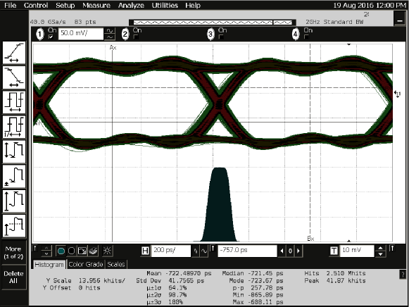
The circuit was tested at a frequency of 1 GHz with a supply of 1.2 V. The circuit consumes 145 A of current at this frequency. First, the DFE feedback factor was set as zero and the offset was swept to find the code which showed the widest bath tub. After the offset code was found the DFE tap was increased and the bath tubs were measured again. Fig. 10 shows the bath tub plots obtained for various values of the DFE feedback factor.
The wider bath tubs correspond to higher values of the feedback factor. The width of the bath tub increases by 15% for the highest tap weight. Fig. 11 shows the eye diagram of the recovered data when the data is sampled at the minimum BER sampling instant.
From layout extracted simulations, the loop delay is found to be 350 ps.
5 Conclusions
In this paper, we report a low latency DFE circuit with integrated offset compensation, built around a sense amplifier comparator with a switched capacitor feedback network. The switched capacitor circuit uses signals from the first stage of the sense amplifier comparator for selecting from precomputed bias voltages, thus resulting in low latency. The bias voltages are programmed for the sum of DFE feeback weight and offset to be corrected. This allows DFE and offset correction with the same feedback input, avoiding an extra offset correction input in the comparator. A 5 bit DAC, along with a little logic circuitry, is used to generate the required four bias voltages. The circuit is designed, fabricated and tested in UMC 130 nm CMOS technology.
Acknowledgements
This work was supported by the Tata Consultancy Services (TCS) in the form of student scholarships and the SMDP programme of the Government of India in the form of CAD tool licenses. The authors would like to thank Nagendra Krishnapura and Shanthi Pavan of IIT Madras, for giving access to the VLSI testing laboratory.
References and Notes
- 1. E. Mensink, D. Schinkel, E. A. M. Klumperink, E. van Tuijl, B. Nauta, Power efficient gigabit communication over capacitively driven rc-limited on-chip interconnects, IEEE Journal of Solid-State Circuits 45 (2) (2010) 447–457. doi:10.1109/JSSC.2009.2036761.
- 2. B. Kim, V. Stojanovic, An energy-efficient equalized transceiver for rc-dominant channels, IEEE Journal of Solid-State Circuits 45 (6) (2010) 1186–1197. doi:10.1109/JSSC.2010.2047458.
- 3. S. H. Lee, S. K. Lee, B. Kim, H. J. Park, J. Y. Sim, Current-mode transceiver for silicon interposer channel, IEEE Journal of Solid-State Circuits 49 (9) (2014) 2044–2053. doi:10.1109/JSSC.2014.2336213.
- 4. S. Kasturia, J. H. Winters, Techniques for high-speed implementation of nonlinear cancellation, IEEE Journal on Selected Areas in Communications 9 (5) (1991) 711–717. doi:10.1109/49.87640.
- 5. Z. Takhirov, B. Nazer, A. Joshi, Error mitigation in digital logic using a feedback equalization with schmitt trigger (fest) circuit, in: Thirteenth International Symposium on Quality Electronic Design (ISQED), 2012, pp. 312–319. doi:10.1109/ISQED.2012.6187511.
- 6. Z. Takhirov, B. Nazer, A. Joshi, Energy-efficient pass-transistor-logic using decision feedback equalization, in: International Symposium on Low Power Electronics and Design (ISLPED), 2013, pp. 335–340. doi:10.1109/ISLPED.2013.6629319.
- 7. M. Sakare, S. P. Kumar, S. Gupta, Bandwidth enhancement of flip-flops using feedback for high-speed integrated circuits, IEEE Transactions on Circuits and Systems II: Express Briefs 63 (8) (2016) 768–772. doi:10.1109/TCSII.2016.2531098.
- 8. B. Nikolic, V. G. Oklobdzija, V. Stojanovic, W. Jia, J. K.-S. Chiu, M. M.-T. Leung, Improved sense-amplifier-based flip-flop: design and measurements, IEEE Journal of Solid-State Circuits 35 (6) (2000) 876–884. doi:10.1109/4.845191.
- 9. K. Naveen, M. Dave, M. S. Baghini, D. K. Sharma, A feed-forward equalizer for capacitively coupled on-chip interconnect, in: 2013 26th International Conference on VLSI Design and 2013 12th International Conference on Embedded Systems, 2013, pp. 215–220. doi:10.1109/VLSID.2013.190.