Quantum transport in graphene Hall bars: Effects of side gates
Abstract
Quantum electron transport in side-gated graphene Hall bars is investigated in the presence of quantizing external magnetic fields. The asymmetric potential of four side-gates distorts the otherwise flat bands of the relativistic Landau levels, and creates new propagating states in the Landau spectrum (i.e. snake states). The existence of these new states leads to an interesting modification of the bend and Hall resistances, with new quantizing plateaus appearing in close proximity of the Landau levels. The electron guiding in this system can be understood by studying the current density profiles of the incoming and outgoing modes. From the fact that guided electrons fully transmit without any backscattering (similarly to edge states), we are able to analytically predict the values of quantized resistances, and they match the resistance data we obtain with our numerical (tight-binding) method. These insights in the electron guiding will be useful in predicting the resistances for other side-gate configurations, and possibly in other system geometries, as long as there is no backscattering of the guided states.
I Introduction
Quantum Hall measurements Zhang et al. (2005); Novoselov et al. (2005) in graphene Novoselov et al. (2004) revealed the relativistic nature of its charge carriers and the gapless spectrum. Long before the discovery of graphene, it was known that carriers in a conventional two-dimensional electron gas (2DEG) tend to move along snake like paths when exposed to inhomogeneous magnetic fields, the so called snake states.Müller (1992); Reijniers and Peeters (2000) Similar effects were explored even earlier in the studies of electron propagation on the boundary of magnetic domains in metallic systems. Rozhavsky and Shekhter (1973); Cabrera and Falicov (1974a, b); Zakharov and Mankov (1984) Experiments in non-planar 2DEGBykov et al. (2000) and in systems with ferromagnetic stripeNogaret et al. (2000) indirectly measured the effects of snake states on the longitudinal and the Hall resistances. In graphene, theoretical predictions of snake-state effects Oroszlány et al. (2008) were quickly followed by experiments which confirmed their existence. Williams and Marcus (2011) Snake states in a Hall bar geometry were previously studied in Ref. Milovanović et al., 2013 using a classical billiard model. A top-gate was used to create a junction along the main diagonal of the Hall cross, and oscillations of the bend resistance were connected with electron guiding along the snake-like paths at the interface.
In this paper we study quantum transport of electrons in graphene Hall bars surrounded with four side-gates (see Fig. 1). The gates modify the local electron density on the edges of the Hall bar, and induce a local electric potential. If the system is placed in an external magnetic field, this edge potential guides the charge carriers along specific equipotential lines. For weak fields, these states move along the previously mentioned snake-like paths, while for stronger fields, we prefer to call them guided states. Our main goal is to understand how this guiding occurs locally, and which paths the electron takes inside the system. Our second goal is to predict the experimentally measurable effects of this guiding. We start by investigating how the side-gate potential modifies the dispersion relations of the electrons in each lead. By studying the current density profiles of the incoming and outgoing states in two representative leads, we are able to build a physical picture of electron transport in this inhomogeneous system. This picture, in combination with the Landauer-Büttiker formalism, allows us to analytically predict the quantization of the bend and Hall resistances. The quantized resistance values match the ones that we obtain with our numerical, tight-binding method. Although we choose one specific potential configuration, with asymmetrically biased side-gates, our results are equally extendable to other gate configurations, and possibly even to other geometries.
This paper is organized as follows: In Section II we describe our system and our numerical methods. Section III is divided in four parts. In the first part (III.1) we analyze the dispersion relations of the leads, and in the second (III.2) we show how guided states look in real space. A scheme for electron guiding is presented in the third part (III.3), and we use this scheme to analytically calculate the bend and the Hall resistances in the last subsection (III.4). Our conclusions are given in Sec. IV.
II System and Methods
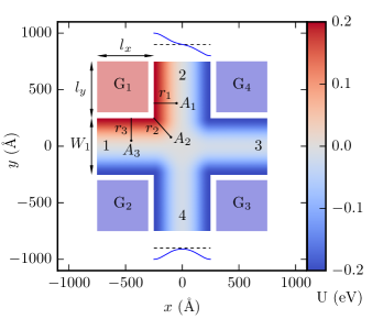
The studied system is shown in Fig. 1, it is a graphene cross with four side gates (, , , ) placed between four orthogonal leads. When biased, the gates create a local potential at the system edges, which decreases towards the interior of the system. We model the potential of a single side gate by a Gaussian function
| (1) |
where is the minimal distance from the present point to the system edge (see Fig. 1). The width of the potential is set to 10 nm, so that potentials of neighbouring gates do not overlap. We use as a reference gate, and potentials of all other gates (, , and ) are set opposite to that of the , as shown in Fig. 1.
For our numerical calculations we use KWANT, a software package for quantum transport simulations based on the tight-binding model.Groth et al. (2014) Graphene is modeled in KWANT using the tight-binding Hamiltonian
| (2) |
where and are the electron creation and annihilation operators, and is the value of the total gate potential () on the -th carbon atom. The hopping term is defined using the electron hopping energy eV, and the Peierls phase factor
| (3) |
where is the vector potential. The vector potential in the horizontal leads is set using the Landau gauge , and that in the vertical leads is . These two potentials are smoothly connected in the main scattering region using the procedure described in Refs. Baranger and Stone, 1989; Shevtsov et al., 2012.
III Results
III.1 Dispersion relations
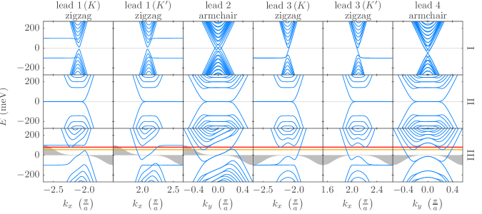
First we study the dispersion relations (presented in Fig. 2) of the side-gated graphene leads. We compare three cases with different combinations of the side-gate potential and magnetic field. Dispersion relations without magnetic field or external potential were extensively studied in Refs. Nakada et al., 1996; Brey and Fertig, 2006a, and therefore we do not present them here. Dispersions for a nonzero potential () and without magnetic field are shown in the first row in Fig. 2. In our previous work Petrović and Peeters (2015) on quantum point contacts we investigated the dispersion relations of symmetrically gated leads, where the same Gaussian potential as given by Eq. (1) was used. Here, for zigzag leads, we focus on a narrow wave-vector range in close proximity of the two valleys ( and ). The potential on the edges determines the energy of the dispersionless bands. In case of a symmetric potential, as in the lead, dispersionless bands shift in energy to a value of . On the other hand, in asymmetrically gated lead, side-gates open a small energy gap between the two flat bands. The gap energy is determined by the lead width. In armchair leads, the asymmetric potential in the lead preserves the electron-hole symmetry, while the symmetric potential in the lead moves the Dirac point towards negative energies.
Results for a nonzero magnetic field and no gate potential (second row in Fig. 2) are explained in Ref. Brey and Fertig, 2006b. In this case, both armchair and zigzag leads show dispersionless surface states, appearing exactly at the energy of the Landau levels (LLs). In this regime, graphene exhibits specific quantization of the Hall resistance, as it was measured in Refs. Zhang et al., 2005; Novoselov et al., 2005.
The most relevant case for us is when both magnetic field and side-gate potential are present in the system (third row in Fig. 2). First noticeable difference introduced by the side-gates is a twisting of the otherwise flat bands of the surface states (compare the second and the third row in Fig. 2). As a consequence of this twisting, surface states become dispersed, and new states appear in the bulk. As we show below these states appear only in specific areas of the sample. In general the symmetry of the lead potential is reflected in the lead dispersion. We plot the potential profiles of each lead in the third row of Fig. 2 (gray areas) to show this connection. Asymmetrically gated leads (the and the lead) have asymmetric dispersions, while symmetrically gated leads (the and the lead) have symmetric dispersions. For symmetrically gated leads this connection can be explained in the following way: suppose we are interested in how the dispersion relation changes when, instead along the lead, we look in the opposite direction (towards the system). To do this we have to invert the potential profile relative to the middle line of the lead. In the inverse space (the space of wave vectors ), this view change is equivalent to inverting the dispersion relative to the axis (all values go to , and the opposite). If the lead potential is symmetric, then this change of view has no effect. We would obtain the same potential and the same dispersion relation. In other words, the inverted dispersion is equal to the initial one . This is the case with the and the lead.
For asymmetrically gated leads, this connection between the lead potential and the dispersion is not so straightforward. If magnetic field is sufficiently strong, the states moving along the opposite edges are completely separated. These opposite edge states then feel different potentials. For example, in the lead for zero potential, electron states with positive velocity (and positive ) move along the left edge, while electrons with negative velocities (and negative ), move along the right edge. For holes, states with positive (and negative velocities) move along the left edge, while states with negative (and positive velocities) move along the right edge. From this we see that states with positive always move along the left edge, while states with negative always move along the right edge. Therefore, if we apply a potential on the left edge, it will only affect the states with positive , while if we only apply a potential on the right edge, it will only influence the states with negative . Assuming that an electron state with positive is shifted in energy (due to the side gate potential) by some value , then electrons with negative are shifted by -, as well as hole states with the same negative . From here, we see that the dispersion is asymmetric . This explanation is similar with the one given in chapter IV in Ref. Datta, 1995.
Before we proceed to the next part, we would like to stress one very important difference between armchair and zigzag leads. Although the minimal band energies appear to be similar for all leads, they are not precisely equal. The minimal band energy in armchair leads is slightly smaller than in the zigzag leads. The red and orange lines in the last row in Fig. 2 show this small misalignment. This difference introduces additional complexity in the system, since a new mode can open in one lead, but electrons can not travel to the neighbouring lead, since there are no open states there. Further below, we explain the importance of this misalignment in more detail.
III.2 Incoming and outgoing modes
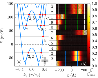
To better understand the motion of charged particles in the system, here we analyze the incoming and outgoing modes of two representative leads: one with symmetric (the lead), and one with asymmetric (the lead) side-gate potential. We focus on studying the evolution of the current profiles in each lead with increaseing Fermi energy.
In Fig. 3(b), we present the current density profiles (insets from 1 to on the right side of Fig. 3) for the incoming modes (red circles in Fig. 3(a)). As we previously mentioned, because of the potential symmetry, the dispersion relation is also symmetric. Therefore the current density profiles for the outgoing modes can be obtained by inverting the profiles shown in Fig. 3 along the middle line of the lead (). We can differentiate two groups of outgoing states in Figs 3(a) and 3(b): (1) the normal edge states (e.g. states 1, 4, and 9), and (2) the guided states (e.g. states , and ) which move along the specific equipotential lines. The electron kinetic energy along these equipotential lines match the energy of Landau levels . For symmetric potential, two of these equipotential lines appear on the system edges for each new appearing LL, and with increasing Fermi energy these lines move towards the middle of the lead (). If the applied potential is smaller than the energy difference between two neighbouring LLs, then a pair of these equipotential lines appear simultaneously for each LL. For example, in Fig. 3, the energy difference between the LL and the LL is smaller than the applied side-gate potential. Therefore, the equipotential lines for the and the LL coexist at higher Fermi energies (green and white lines in insets 8– in Fig. 3(b)). Because of the symmetry of the side-gate potential, these equipotential lines always appear in pairs: the line on the right side correspond to guided electrons coming out of the lead, while the line on the left corresponds to guided electrons coming into the lead. Each of these lines can accommodate two states coming from different valleys (in armchair leads this is not so obvious, because there are no separate valleys, but in zigzag leads each guided state can be connected with a specific valley). For the zeroth LL, the guided states are always centered on the equipotential line (states going along the blue lines in insets 2, and 3 in Fig. 3(b)), while for higher LLs there is significant broadening of the guided states (states going along the green lines in insets , and in Fig. 3(b)). Similar behaviour was reported in Ref. LaGasse and Lee, 2016.
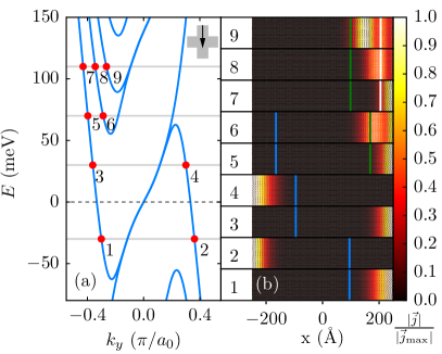
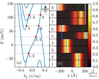
The case for an asymmetric potential is presented in Figs. 4, and 5. Here, because of the asymmetry, the outgoing modes are not equivalent to the incoming ones, and therefore it is necessary to study them separately. In contrast to symmetrically gated leads, here for each LL there is only one equipotential line satisfying the condition . For each new LL this line appears first on the right edge, and moves towards the left edge as we increase the Fermi energy (see the blue lines in insets 1–6 in Fig. 4(b)). For the zeroth LL, these blue lines mark the separation point between electron and hole edge states (a border). For higher Fermi energies (, and meV), the hole edge state on the left side disappears, and as we see below, it is replaced with an electron edge state moving in the opposite direction. Although there are no guided states among the incoming modes in Fig. 4, they appear among the outgoing modes in Fig. 5. The electrons are guided along the equipotential lines of the zeroth and the first LL, similarly as in the symmetric potential case (for example, compare insets 1, 2, 5, 7, and 8 in Fig. 5(b), with insets 2, 3, 7, , in Fig. 3(b)).
Although we only considered current profiles of the armchair leads, the corresponding incoming and outgoing modes in the (horizontal) zigzag leads are very similar. The only difference is that in zigzag leads each guided state can be connected with one of the valleys. The opening and closing of modes in neighbouring leads do not occur at the same energy, because of a small subband misalignment mentioned above. There are situations where only one of the two guided states passes to the neighbouring lead, while the other guided state is backscattered, because there is no open outgoing mode in the neighbouring lead.
III.3 Current guiding
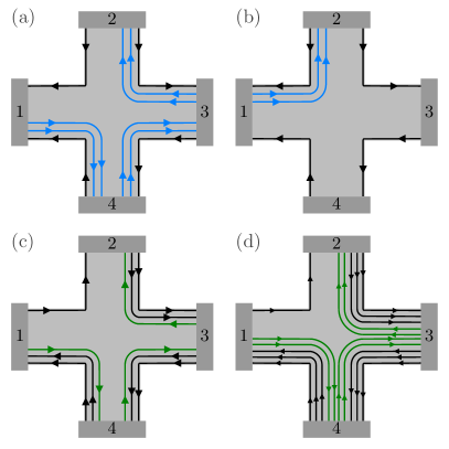
The analysis of incoming and outgoing modes allows us to construct a picture of electron transport in this system. By extending previous results from the vertical (armchair) leads to the horizontal (zigzag) leads, in Fig. 6 we present a constructed scheme for electron guiding.
At the lowest energy ( meV, Fig. 6(a)), for each edge state on the negatively biased edges, there is a pair of guided states moving in the opposite direction. The guided states move along the interface (the blue lines). Although there is only one interface with two identical guided states on it, here we show two separate blue curves in Fig. 6(a) to emphasize that there are two guided states. The position of these lines in the scheme do not match the actual position of the interface. As Fermi energy increases, the interface shifts towards the central lines of the cross, and for positive Fermi energies, the interface moves to the upper-left part of the system. This is what we see in Fig. 6(b), for meV. The two guided states are close to the hole state on the upper-left edge. For larger Fermi energies, the hole state on the upper-left edge disappears, and the pair of guided states turns into a single electron edge state, moving upwards along the upper-left edge (as in Fig 6(c)).
Due to the above mentioned mismatch of the band minimal energies in neighbouring leads, the case when the Fermi energy is meV is one of those situations where new modes open in the vertical (armchair) leads, but they backscatter due to the lack of open states in the horizontal (zigzag) leads. Therefore the scheme presented in Fig. 6(c) corresponds to larger energies (e.g meV) when guided states open in all four leads. This situation is very similar to that presented in Fig. 6(a), except now there is only one guided state along the interface. As the Fermi energy further rises ( meV, Fig. 6(d)), a new edge state and a new guided state appear in the system.
The scheme presented in Fig. 6 can be generalized to higher LLs, assuming that the applied potential is smaller than the energy difference between the neighbouring LLs. For -th LL (), on the negatively biased edges there will be or edges states, and one or two guided states, while on the positively biased edges, there will be edge states. However, for every value , no matter how small it is, there will always be some minimal for which all higher LLs () are separated by an energy smaller than the applied potential. The present scheme is more complicated for these higher LLs, because guided states from several LLs can coexist at the same Fermi energy. We do not consider these cases here.
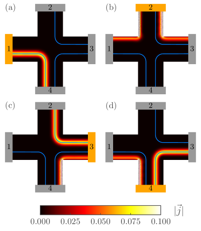
To confirm the correctness of the scheme presented in Fig. 6, we show in Fig. 7 the current density profiles for all four leads at the Fermi energy meV, as obtained from our numerical solution using KWANT. By combining all the currents presented in Fig. 7, we get the same picture as that presented in Fig. 6(a).
III.4 Bend and Hall resistances
Based on the pictures presented in Fig. 6, we are able to calculate the band resistance by applying the Landauer-Büttiker formula. The most important property of the guided states is that they fully transmit without any backscattering. In that sense, they are equivalent to edge states. As long as there is no backscattering, the transmission coefficients are integers and the transmission matrix is easy to write by hand by counting the incoming and outgoing modes.
To calculate the resistance, we select one of the insets in Fig. 6, for example 6(d), and write the current matrix
| (4) |
Here is the conductance quantum, and we choose (for details see Chap. IV in Ref. Datta, 1995). Here we are only interested in the bend resistance
| (5) |
when current is passed from the first into the second lead (the currents are ). From the second row of Eq. (4) we obtain , and from the third row we obtain
| (6) |
and therefore . Substituting this back in the first row in Eq. (4), we obtain
| (7) |
and therefore , and . Finally, we can calculate the resistance as
| (8) |
In a similar manner, we can calculate the quantized resistances for the other situation depicted in Fig. 6. For Fig. 6(a) we obtain , and for Fig. 6(c) we also obtain . For Fig. 6(b) there is only one edge state connecting the and the lead, therefore the potential on these two leads is equal ().
Previous calculations can be generalized for higher LLs. Assuming that applied potential is smaller than the separation between the neighbouring LLs, we can differentiate two cases. In the first case, there is only one guided state open in each negatively biased lead (equivalent to Fig. 6(c)), while in the second case there are two such guided states (equivalent to Fig. 6(d)). In the first case, the general current-voltage matrix relation
| (9) |
can be expressed in terms of LL index . When solved, this gives the quantized resistances
| (10) |
For the second case, when both guided states are present in the system, the general Landauer-Büttiker matrix is
| (11) |
which gives
| (12) |
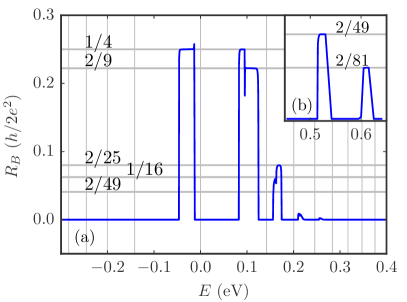
Comparison between numerical and analytical results is presented in Fig. 8. Quantized resistances obtained analytically agree well with the ones obtained numerically, at least for the first three Landau levels in Fig. 8(a). For higher Landau levels, the match is not exact (see for example the line for in Fig. 8(a)). We suspect that the reason for this mismatch is a spatial widening of the guided states for higher LLs, which might lead to some backscattering. A comparison with the band resistance obtained for higher field and weaker gate potential in Fig. 8(b) reveals that the calculated resistance still matches the analytically obtained fractional values. Also the stronger field appears to better align the minimal band energies, since we do not observe the generalized quantized values , where only one guided state is present in the system. Another characteristic of is that is not symmetric for electrons and holes. Plateaus appear only for zero and positive LLs. A narrow positive peak near the right corner of the first plateau, and a negative peak between the 1/4 and 2/9 plateaus originate from a small misalignment of subbands in the horizontal leads. Although gates and induce equal potential on the lower edge in the first and the third lead (see Fig. 1), this potential is slightly modified by gates on the upper edges (gates and ). Subbands are misaligned because of this small potential difference on the lower edge.
Results for the Hall resistance are presented in Fig. 9, for the same magnetic field and side-gate potential as in Fig. 8(a). Under the same conditions as in the case of the bend resistance, we can calculate the quantization values for the Hall resistance. The conductance matrix is the same as given by Eqs. (9), and (11). But now the current is injected in the first lead and collected in the third lead (the current column is ). The Hall resistance is calculated analytically as , because . For the two cases, we obtain
| (13) |
and
| (14) |
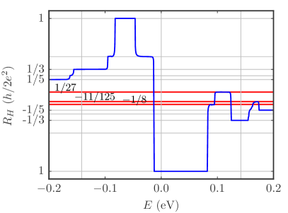
In Fig. 9, we compare the first three analytic results with the numeric ones. The main feature of the Hall resistance is that side gate potential separate the two valleys. Instead in steps of , the plateaus are separated by (see horizontal grey lines).
IV Conclusions
In conclusion, we investigated the quantum electron transport in side-gated Hall bars in high magnetic fields. Starting from the lead dispersion relations which reveal new states appearing in the Landau spectrum, we proceeded to study the current density profiles of these new states in two representative leads. Spatially, the new states are guided along equipotential lines where the electron kinetic energy matches the energy of a LL. Due to a full transmission of these states, the transmission matrix contains only integers and can be solved analytically. We calculated the quantized resistances for this asymmetric gate configuration and obtained
and
for the bend resistance in two cases, when there is only one and when there are two guided states. For the Hall resistance we obtain
and
The calculated quantized resistances match the quantized resistances obtained with the tight-binding method. Note that these results can be easily extended to symmetrically gated Hall bars, where potential is the same on all four gates. Also the derived pictures of electron guiding can be applied to other geometries with a side potential, since in general for every pair of edge states entering the system there will be a pair of guided states moving in the opposite direction.
V Acknowledgements
This work was supported by the Methusalem programme of the Flemish government. One of us (F. M. Peeters) acknowledges correspondence with K. Novoselov.
References
- Zhang et al. (2005) Y. Zhang, Y. W. Tan, H. L. Stormer, and P. Kim, Nature 438, 201 (2005).
- Novoselov et al. (2005) K. S. Novoselov, A. K. Geim, S. V. Morozov, D. Jiang, M. I. Katsnelson, I. V. Grigorieva, S. V. Dubonos, and A. A. Firsov, Nature (London) 438, 197 (2005).
- Novoselov et al. (2004) K. S. Novoselov, A. K. Geim, S. V. Morozov, D. Jiang, Y. Zhang, S. V. Dubonos, I. V. Grigorieva, and A. A. Firsov, Science 306, 666 (2004).
- Müller (1992) J. E. Müller, Phys. Rev. Lett. 68, 385 (1992).
- Reijniers and Peeters (2000) J. Reijniers and F. M. Peeters, J. Phys. Condens. Mat. 12, 9771 (2000).
- Rozhavsky and Shekhter (1973) A. S. Rozhavsky and R. I. Shekhter, Solid State Commun. 12, 603 (1973).
- Cabrera and Falicov (1974a) G. G. Cabrera and L. M. Falicov, Phys. Stat. Sol. (b) 61, 539 (1974a).
- Cabrera and Falicov (1974b) G. G. Cabrera and L. M. Falicov, Phys. Stat. Sol. (b) 61, 217 (1974b).
- Zakharov and Mankov (1984) Y. V. Zakharov and Y. I. Mankov, Phys. Stat. Sol. (b) 125, 197 (1984).
- Bykov et al. (2000) A. A. Bykov, G. M. Gusev, J. R. Leite, A. K. Bakarov, N. T. Moshegov, M. Cassé, D. K. Maude, and J. C. Portal, Phys. Rev. B 61, 5505 (2000).
- Nogaret et al. (2000) A. Nogaret, J. S. Bending, and M. Henini, Phys. Rev. Lett 84, 2231 (2000).
- Oroszlány et al. (2008) L. Oroszlány, P. Rakyta, A. Kormányos, C. J. Lambert, and J. Cserti, Phys. Rev. B 77, 081403 (2008).
- Williams and Marcus (2011) J. R. Williams and C. M. Marcus, Phys. Rev. Lett. 107, 046602 (2011).
- Milovanović et al. (2013) S. P. Milovanović, M. R. Masir, and F. M. Peeters, Appl. Phys. Lett. 103, 233502 (2013).
- Groth et al. (2014) C. W. Groth, M. Wimmer, A. R. Akhmerov, and X. Waintal, New J. Phys. 16, 063065 (2014).
- Baranger and Stone (1989) H. U. Baranger and A. D. Stone, Phys. Rev. B 40, 8169 (1989).
- Shevtsov et al. (2012) O. Shevtsov, P. Carmier, C. Petitjean, C. Groth, D. Carpentier, and X. Waintal, Phys. Rev. X 2, 031004 (2012).
- Nakada et al. (1996) K. Nakada, M. Fujita, G. Dresselhaus, and M. S. Dresselhaus, Phys. Rev. B 54, 17954 (1996).
- Brey and Fertig (2006a) L. Brey and H. A. Fertig, Phys. Rev. B 73, 235411 (2006a).
- Petrović and Peeters (2015) M. D. Petrović and F. M. Peeters, Phys. Rev. B 91, 035444 (2015).
- Brey and Fertig (2006b) L. Brey and H. A. Fertig, Phys. Rev. B 73, 195408 (2006b).
- Datta (1995) S. Datta, Electronic Transport in Mesoscopic Systems (Cambridge University Press, 1995).
- LaGasse and Lee (2016) S. W. LaGasse and J. U. Lee, Phys. Rev. B 94, 165312 (2016).