Machines and Algorithms
Abstract:
I discuss the evolution of computer architectures with a focus on QCD and with reference to the interplay between architecture, engineering, data motion and algorithms. New architectures are discussed and recent performance results are displayed. I also review recent progress in multilevel solver and integation algorithms.
1 Introduction
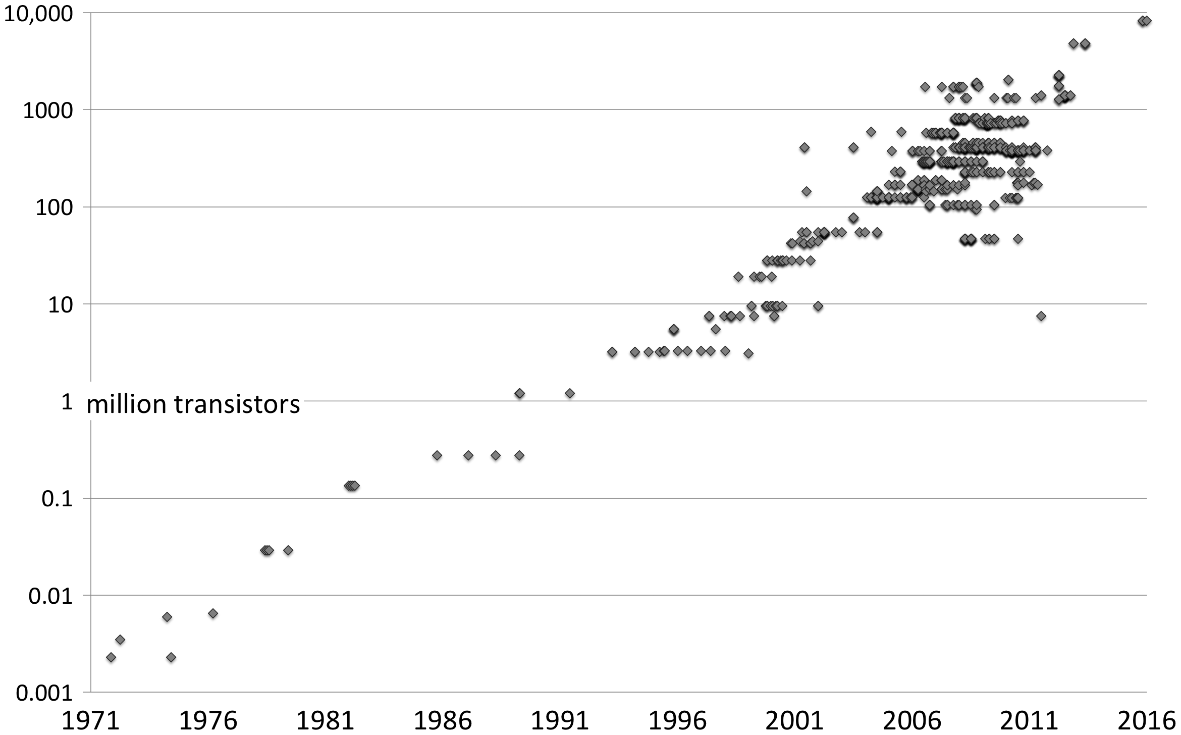
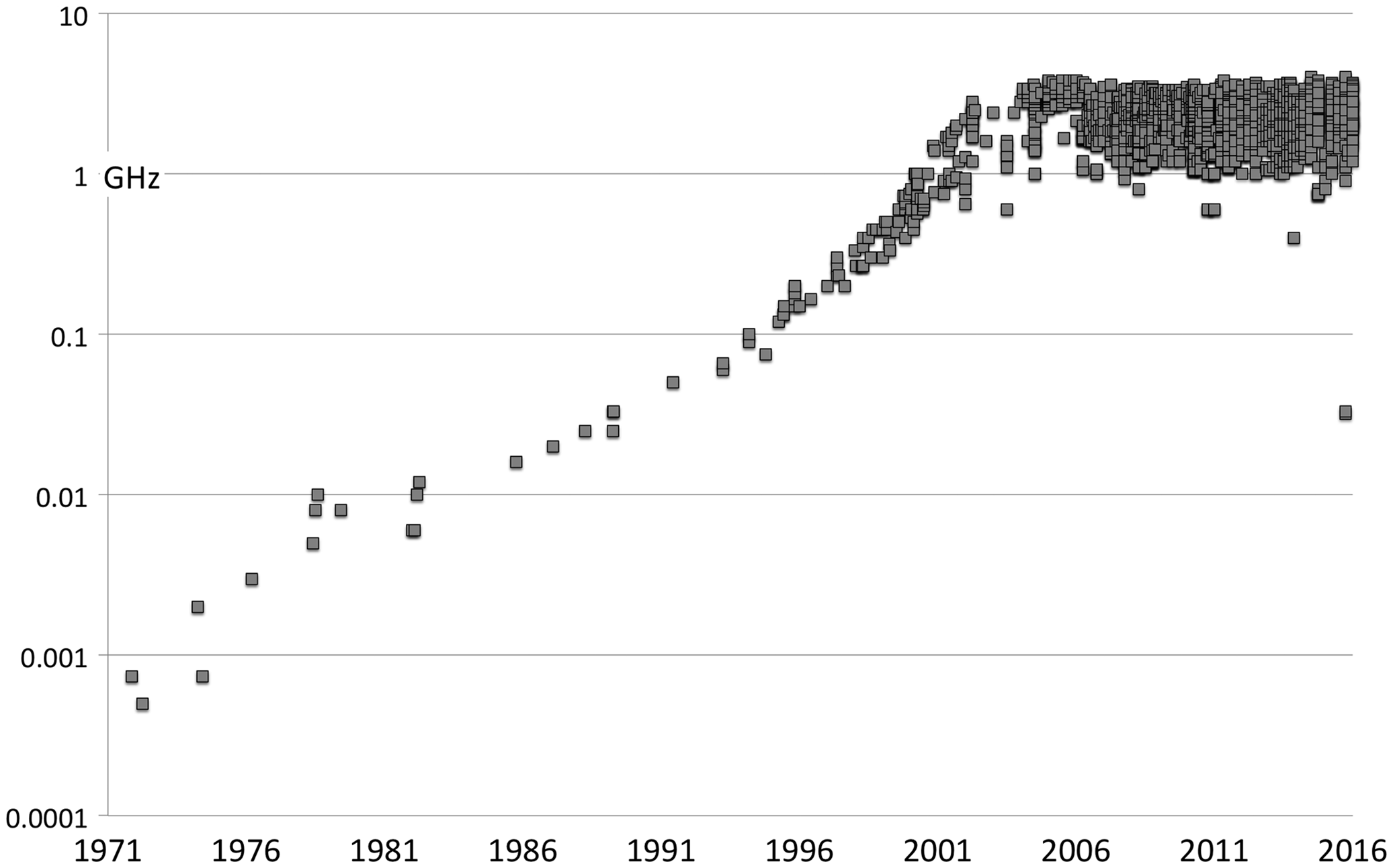
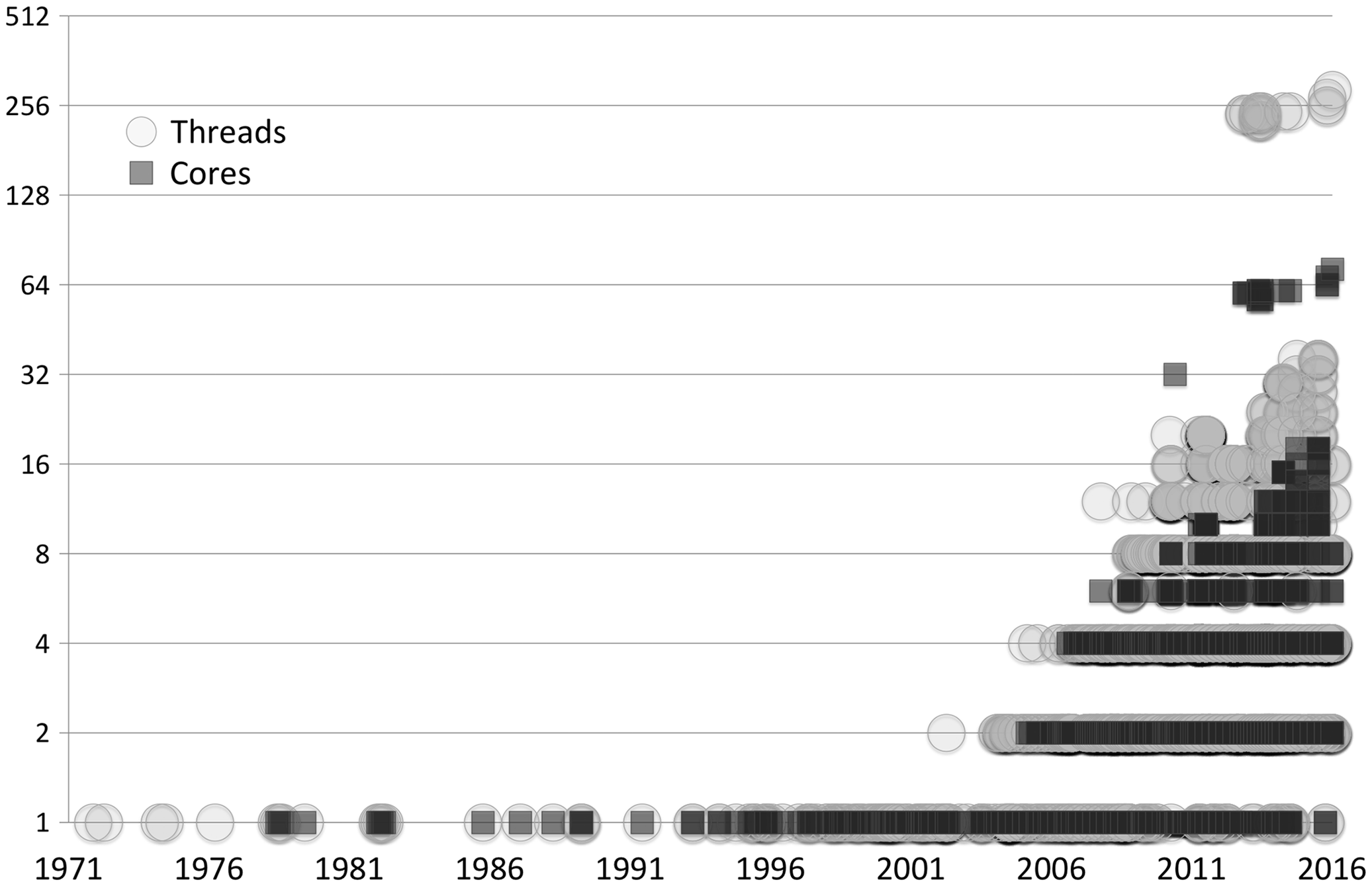
Present roadmaps for the evolution of computing paint a rather mixed picture for the scientific programmer: computer power continues to grow rapidly. However this growth increasingly arises solely through the expansion of many forms of parallelism, rather than improving serial execution speeds. This is manifested, Figure 1, by a continued growth in transistor and hence core counts, but no longer accompanied by greater clock frequencies. These figures are reproduced from ref [1].
The sheer pain of efficiently programming increasingly complex devices is daunting, particularly since the industry standard solution appears to be to dump it on the programmer. The forms of parallelism include message passing interfaces for treating distributed memory multi-processing (e.g. MPI), thread level parallelism (OpenMP, CUDA), and single-instruction-multiple-data (SIMD) short vector instructions.
| Core | simd | Year | Vector bits | SP flops/clock/core | cores | flops/clock |
|---|---|---|---|---|---|---|
| Pentium III | SSE | 1999 | 128 | 3 | 1 | 3 |
| Pentium IV | SSE2 | 2001 | 128 | 4 | 1 | 4 |
| Core2 | SSE2/3/4 | 2006 | 128 | 8 | 2 | 16 |
| Nehalem | SSE2/3/4 | 2008 | 128 | 8 | 10 | 80 |
| Sandybridge | AVX | 2011 | 256 | 16 | 12 | 192 |
| Haswell | AVX2 | 2013 | 256 | 32 | 18 | 576 |
| KNC | IMCI | 2012 | 512 | 32 | 64 | 2048 |
| KNL | AVX512 | 2016 | 512 | 64 | 72 | 4608 |
| Skylake | AVX512 | 2017(?) | 512 | 96 | 28 | 2688 |
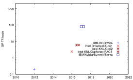
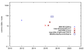
Further, in addition to complex but solvable programming challenges, Table 1, there are fundamental limitations on the flexibility of future systems imposed by changes in relative performance of floating point execution to the bandwidth to caches, memory and interconnects. A timeline for the evolution of system performance, performance per node, and interconnect performance is collated in Figures 2 and 2. We can see that the four hundred fold project increase in single node performance in a few years is accompanied by only a two fold increase in interconnect bandwidth. As a consequence, business as usual is not an option for algorithms. We take as a starting point with machines such as today’s BlueGene/Q system are very much in balance for scalable QCD simulation, and plot the future evolution from published roadmaps of system arithmetic peak, single node arithmetic peak, and single node bidirectional network bandwidth in Figure 2 and Figure 2.
2 Technology directions
I first discus the evolution and trends in the basic electronic engineering technologies that underpin the development of computing. These represent the constraints within which vendors must operate. On a point of principle it is worth emphasizing that our relations with vendors can be positive, but we must understand each other clearly. Our interests are only aligned when it comes to ensuring the best possible products. Vendors have a requirement to maximise their profit, while scientists have a requirement to maximise our scientific return, to a certain extent by minimising vendor profit. Market segmentation techniques are the enemy of scientists, since these attempt to increase the price per core or Teraflop as the aggregate capability per node or system increases. In short, we wish to perform our science at computer game pricing.
It is greatly to the benefit of science to ensure that the existence of a volume commodity market in similar parts improves our science, rather than commercial profit margins while we buy the expensive version. This does imply that scientists should always maintain a credible ability to use commodity parts. Our ability to do so is limited by reliability of low end “non server” parts, and by the cost of efficiently interconnecting them. If the price differential is too great however, we must bear in mind that we have the option of verifying solutions and/or recalculating a second time.
Wire delay: Some simple physics explains much of these computer architecture trends. We can model a wire as a rod of metal of volume . Applying Gauss’s law,
and the resistance and capacitance are
This gives rise to the discharge time constant
This is profound, because to a great degree (ignoring logarithmic terms and finite size effects) wire delay depends only on the geometry or aspect ratio of the wire. Sadly, shrinking a process by the same scale factor in all dimensions does not speed up wire delay. Wire delay places an irreducible floor below which faster transistors make no difference. It is interesting to note that historically process advances announced in the press have included materials changes designed solely to move this wire delay floor out of the way of transistor scaling: “copper interconnect” (180nm) and “low-k“ dielectric (100nm) improved and respectively changing the RC timeconstant. Anecdotally, the author participated in the design of memory prefetch engine for BlueGene/Q in IBM’s 45nm process. The slowest timing path in this component was roughly 50% wire delay and 50% transistor delay; this balance becomes worse as transistors become faster without changes to the materials that control wire delay.
The immediate corollary of the aspect ratio dominance of wire delay is the following: Multi-core design with long-haul buses only possible strategy for 8 Billion transistor devices. There must be a low number of long range “broad” wires (bus/interconnect) since these consume area, and a high number of short range “thin” wires giving densely connected regions (cores).
Memory technologies: Data motion is often the single greatest performance and power bottleneck to be addressed in computation. A nuanced approach to analysing code will distinguish data references by their most likely origin (e.g. cache, local memory, remote node). For a bandwidth analysis, the ratio of the floating point instructions executed to the bytes accessed for each of the cache, memory and interconnect subsystems is called the arithmetic intensity of the algorithm and is a key classfication to understand if a computer is engineered to support efficient execution of the algorithm. Since the cost of floating point units has decreased exponentially, while the cost of macroscopic copper traces has remained (relatively) static, it is often the case that execution is memory limited. The term memory wall has been coined representing a latency bound on execution throughput[5], and can impose a bound on throughput that can only be addressed by changes to the speed of light. Fortunately, for deterministic algorithms, hardware or software prefetching can move the problem to a bandwidth problem that succumbs to investment, and many scientific algorithms can be categorised as either bandwidth or FPU bound, for example using the Berkely roofline model[6].
One important application of the previous simple analysis of wire delay arises when we consider connection of a calculation device to memory chips. Long copper traces across a printed circuit board fall into the precisely the worst case corner for wire delay. Further, given the speed of light and GHz scale clock rates distances of order 30cm (= 1 light-nanosecond) set the length scale at which transmission line behaviour sets in.
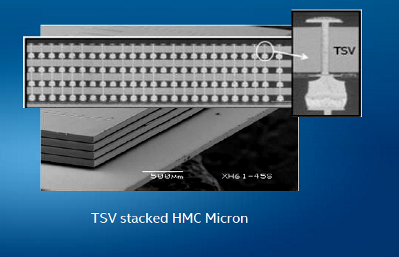
In order to substantially address memory limitations it is necessary to both change the aspect ratio of the wires involved, and vastly increase the number of wires that can carry data concurrently. Fortunately the computing industry has already invested in technology directions responding to this imperative; the most significant standards are the “High Bandwidth Memory” (HBM), “Hybrid Memory Cube” (HMC), and “WideIO” as well as some proprietary interfaces. Memory chips have been developed with large numbers of vertical rods (through silicon vias or TSV’s) used as high bit count buses skewering the device, Figure 3. The ability to stack such chips vertically, with solder connections between TSV’s giving a favourable aspect ratio, low wire delay and power. Further the miniaturisation enables a high lane count connection that gives a massive data rate for reading memory pages; it is exciting that after decades of conservatism in memory design, there is no clearly defined barrier to further increases in the number of bitlanes.
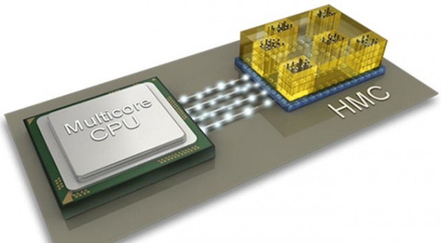
This is driving a rather revolutionary development across the industry towards on package integration of memory, where a sizable volume of memory is physically colocated with the processing unit. This may be done either through 2.5D integration with memory stacks placed along side a processing unit on an interposer (i.e. a miniature circuit board), or full 3D integration where memory chips are bonded on-top of a processing unit using TSV’s.
The HMC and HBM solutions are presently 2.5D and either exposed with high bit count and (relatively) low data rate per bit lane (HBM) to a memory controller on a processing unit, or in the case of HMC interfaces through a base layer logic chip that provides a high bit rate and low lane count interface to the processing unit. Full 3D memory solutions could, in principle, yield significant growth of bus widths in future, since the mechanical assembly for high density TSV’s is fundamentaly different to the decades old PCB copper trace problem.
A further significant emerging memory technology is a novel form of non-volatile phase change memory, typically based on an amorphous/crystaline glass cell. This should enable to increase memory density, and in particular is suggested to support many bit-cells vertically stacked in multiple layers. Micron and Intel place this under “3D Xpoint” branding and promise four times higher density that DRAM. The most exciting application lies in plans to give such devices conventional DRAM electronic interfaces, but uses will range from solid state disks to potential integration in conventional memory systems. Although details are rather difficult to come by[4]. The author expects that it is a reasonable assumption that once a page is open the column accesses should be no slower than conventional DRAM since the electronics will be similar, while page miss latency may be larger. Certainly there are already multiple JEDEC NVDIMM standards planned, and NVDIMM is likely a disruptive technology for large memory algorithms, such as the use of Dirac eigenvectors and the assembly of multi-hadron correlation functions.
Interconnect: A very significant trend is the integration of interconnect. Historically, QCD calculations have often been near the frontier of interconnect technology requirements, largely because a four dimensional application with the same data footprint per node suffers from worse surface to volume ratio than lower dimensional applicaton. As a result, integration of interconnect has been pioneered by QCD machines such as QCDSP and QCDOC[10], and also by the IBM BlueGene line[11]. If the integration is performed on a compute ASIC, the additional cost for interconnect can be reduced from thousands of dollars to pennies per node particularly if novel rack integration keeps most traces in copper backplanes and driven by integrated transceiver logic.
There are some interesting current trends. Firstly, with the Intel Omnipath interconnect being integrated on package in one variant of the Intel Knights Landing device (KNL-F) and with variants of the Intel Skylake Xeon processor. These use a distinct silicon chip implementation providing two 100Gb/s Omnipath ports, and in the KNL-F is integrated in a multi-chip module package. The marginal cost is claimed to be around $300 per node, but this includes only the cost of the interfaces does not include cable and switch pricing. Further, a second generation Omnipath 2.0 will be integrated with the Knights Hill computer chip planned for the Aurora supercomputer in 2018. The principal competing interconnect technologies are the Mellanox Infiniband product line, which offers excellent performance but typically with a greater per port cost, and the Cray Aries interconnect used in the Cori and Theta supercomputers as an example.
Secondly, Nvidia has announced a novel NVLink technology with a tremendous bandwidth of up to 160GB/s bidirectional per link that scales up 8 GPU’s. However, while providing excellent local bandwidth within a server, this is not a large cluster interconnect, and must be combined with another technology in a large system. For example, the Summit and Sierra systems combining IBM Power hosts with multiple Nvidia GPU’s will make use of Mellanox interconnects between powerful compute.
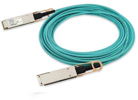
System design and reduced optical cost: System or rack level design can make a large difference to interconnection costs. Due to the attenuation of high speed signals in copper traces, it is unfortunately the case that almost all high performance transmissions over 3m in length must proceed using optical interconnects. A significant design element of the BlueGene/Q system was its high density; by using very dense racking techniques the optical cost was suppressed by the surface to volume ratio. Similar approaches are taken to varying degrees in the Cray Aries and SGI ICE-X architectures, and in more standard blocking fat tree networks.
While 100Gbit/s of copper trace in a larger PCB will cost as little as pennies, the same 100Gbit/s of bandwidth in copper cables costs just under $100 USD. A similarly performing 100Gbit/s active optical cable with four bit lanes costs an eye watering 1000 USD4. It may even be the case that never before in the field of computing have so few bits cost so much! This expense is largely due to the use of copper signalling and active optical transceivers on either end of the cable. The cost is largely in the electronics, and may in future be addressed if silicon photonics allows the integration of the laser transceivers upstream in the computational node. This has the potential to reduce the cost and power of driving fibre cable to be closer to cost of copper, and to use a normal silicon process for laser components.
There is probably a room for an adventurous vendor or even academic project to design a standard cluster but with dense rack packaging and backplane local interconnect, perhaps even using PCI express at the rack level to suppress the cost of interconnect, in a similar style to the BlueGene/Q rack level design, but otherwise using commodity components.
3 Novel hardware platforms
The two significant hardware platforms released in 2016 are the Intel Knights Landing “many-core” processor and the Nvidia Pascal GPU. These give much more parallelism than more conventional nodes from Intel and IBM, and greater power efficiency, and there is considerable community interest in whether the greater peak performance and efficiency translates into delivered application performance for QCD. We survey single node performance results from QCD software development efforts on these chips.
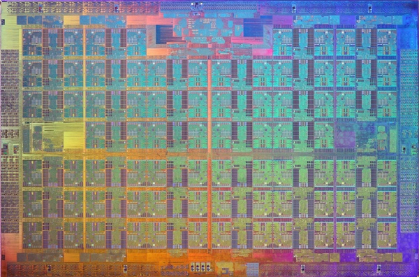
Intel Knights Landing: Intel has introduced the Knights Landing chip[12] makes use of many low power, but architecturally standard, processor cores. The cores can issue up to two instructions per cycle (compared to up to 6 instructions per cycle for high end Xeon cores) and this includes up to two 512 bit wide vector instructions. The devices range from 64 to 72 cores depending on the specific part. The cores execute all legacy x86 instructions such as SSE, AVX and AVX2 but best performance requires targetting the AVX512 instruction set which can be a non-trivial software investment. The peak performance using single precision is over 6 TFlop/s and over 3TFlop/s for double precision.
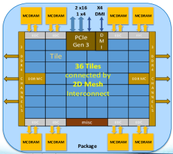
The cores are arrange into tiles each containing a 1MB L2 cache and a pair of cores. These are interconnected through a two dimensional routing mesh, and the system-on-a-chip includes both six DDR4 memory controllers providing up to 384GB of memory (quoted at 90GB/s STREAMS AXPY) and eight on-package chipstacked memory controllers (quoted at 400GB/s STREAMS AXPY) providing 16GB of memory. The high bandwidth memory can either be used in flat mode as a directly addressable NUMA domain under Linux, in cache mode as a very large direct mapped L3 cache, or in hybrid mode as 8GB NUMA domain and 8GB cache.
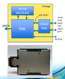
The Knights Landing can be packaged with two ports of 100Gb/s Omnipath interconnect fabric, and unlike the previous Knights Corner chip can be configured as a self hosting compute node, without the need of an accelerator card or offload programming model. This is a substantial simplification for the programmer. A sensible way to programme these chips involves using a hybrid combination of MPI message passing, OpenMP threading and SIMD vectorisation. The nature of modern compilers and some experience suggests that the most effective vector utilisation is obtained when compiler vector intrinsic functions are used, rather than relying on compiler vectorisation of loops.
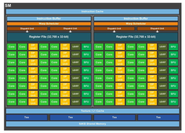
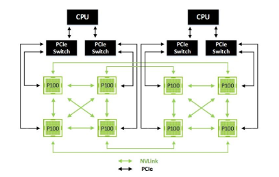
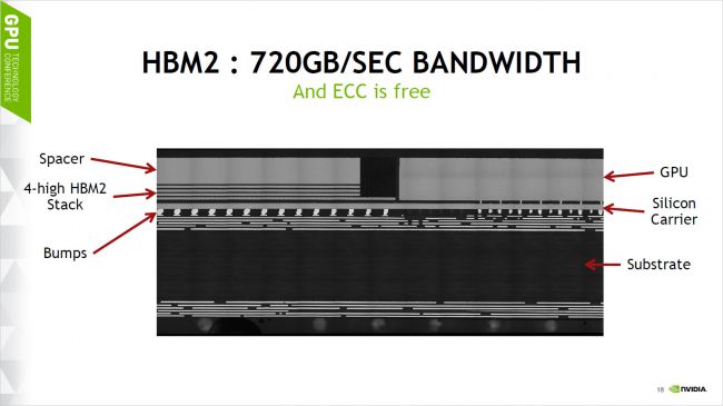
Nvidia Pascal: Nvidia has released the Pascal GPU, with some exciting features and impressive peak single precision performance of 10.6 TF/s, Figure 6. The Pascal uses a form of 3D memory known as HBM2, providing up to 600GB/s Streams AXPY111Figure provided by Kate Clark.. The device supports 64 bit, 32 bit, and 16bit floating point arithmetic, and various reliable update, preconditioning, or mixed precision schemes may be used to accelerate QCD solution without loss of accuracy. The Pascal introduces 4 NVLink ports, Figure 6, per GPU giving up to 160GB/s of bidirectional bandwidth in aggregate across these links. The NVLink ports can be used to interconnect up to eight GPU’s within an Nvidia DGX1 system, and also can accelerate the bottleneck of a slow PCIe I/O bus between up to four GPUs and the host memory (and MPI interconnection) when combined with IBM Power8 nodes in IBM S822LC servers.
In common with earlier GPU versions, the simple cores are only accessible through an offload programming model since they cannot run general code. These are typically accessed through the CUDA programming environment that leverages the C++ language. This has been made accessible for QCD calculations by both the QUDA library [14] and the QDP-JIT library[9]. Single nodes with up to 40 or 80 peak single precision TF/s can be assembled using 4 or 8 GPUs. For many QCD algorithms interconnect performance becomes a key consideration, and communication minimising strategies such as domain decomposition will be important.
In contrast to earlier GPU’s, Pascal introduces a “Page Migration Engine” that can transparently move virtual memory pages between the CPU host and the accelerator card. This introduces a common address space, even if implemented through physical motion, between code executing on the host and on the accelerator. This is potentially a programming model simplification, allowing a single allocator and no explicit data motion. There is great scope for simpler QCD libraries to make use of Pascal and future Nvidia GPU’s leading to more easily performance portable code.
A sensible way to programme systems based on these chips involves using a combination of MPI message passing and CUDA calls. The CUDA code still requires data to be laid out in a SIMD or vector friendly order in order to ensure that single memory transactions are performed for all elements of a SIMD unit; this optimisation is known as read coalescing. As a result, both GPU and many-core CPU code requires layout flexibility to be optimal; however at present it is rather difficult to write computer programmes that support both with best efficiency.
4 Software challenges
Text book computer engineering[8] suggests that code optimisations should expose an admixture of two forms of locality: spatial data reference locality, and temporal data reference locality.
Buses are used that transfer many contiguous words of data at a time in many levels of a computer memory system. For example, When a DRAM page is opened (row access), very many consecutive bit cells are read and page hits (column access) incur much less overhead than a new random access giving rise to different latencies. Further, multiple layers of caches are used; the access bandwidth and latency characteristics become poorer the further one travels from the processor core while the storage capacity correspondingly increases. The transfers between levels in the memory system are performed in aligned chunks called cachelines, with sizes bytes depending on the level and computer architecture. For example, modern Intel chips typically use a 64B cacheline in all layers of the cache hierarchy, while the IBM BlueGene/Q system made use of a 64B L1 line size and a 128B L2 line size.
Spatial reference locality arises because memory systems are fundamentally granular. If one touches and transfers one word of a cacheline, the entire cacheline is transferred over (rate limiting) buses in the system. Algorithms and codes should ensure that they make use of all the data in cachelines that are transferred (by laying out data to give spatial locality of reference) to maximise performance. Architectures use cachelines based on the observation that many algorithms (such as linear algebra) have such access patterns. Temporal locality of reference arises when data referenced is likely to be reference again soon. Thus caches store recently accessed data. Both of these hardware optimisations can be exploited in software by writing scalar loops that loop or block in the right order, and so are relatively easy to exploit.
In contrast, short vector instructions (single instruction, multiple data or SIMD) brings a new level of restrictivness that is much harder to hit. Code optimisations should expose what I will call spatial operation locality. Although there are obvious applications in array and matrix processing, even matrix transposition shows that it is surprisingly hard to exploit in general because you must both arrange to have same operation applied to consecutive elements of data.
However, it is vastly cheaper to build hardware execute a single arithmetic instruction or load on a contiguous block of elements of data than to generally schedule independent and decoupled instructions. As a result, SIMD is one of the cheapest ways to enhance peak floating point performance, particular if the rest of the processor core is rather complex and aggressively optimised. Table 2 displays the decomposition of various current computational chips into processing cores and SIMD execution units.
| Chip | Clock | blocks | per bock | SP madd | issue | SP madd | peak |
|---|---|---|---|---|---|---|---|
| GP100 | 1.4 GHz | 56 SM’s | 2 IB/RF | 32 | 3584 | 10.5 TF/s | |
| KNL | 1.4 GHz | 36 L2 tiles | 2 cores | 32 | 2304 | 6.4 TF/s | |
| Broadwell | 2.5 | 18 cores | 16 | 576 | 1.4 TF/s |
5 QCD computational challenge
We will consider the computational requirements of Wilson, Improved Staggered and Domain Wall fermion actions and with both single right hand side and multiple right hand side Krylov solvers. Multiple right hand side solvers can be advantageous, where applicable, for Wilson and Staggered actions because the gauge field is a significant element of the memory traffic and can be applied to multiple vectors concurrently, suppressing this overhead. The same suppression factor already occurs quite naturally for five dimensional chiral fermion actions such as DWF. When this is combined with block solvers[7], this conference, the gain is amplified and both algorithmic and execution performance can be accelerated. We assume an local volume and either an 8 point (nearest neighbour) or 16 point (nearest neighbour + naik) stencil. Providing the global switching is implemented well in a fat tree switched network, or we map well to the topology of a routing torus, hypercube, or Dragonfly network this will suffice to characterise the performance of a large machine. That is to say under the assumption weak scaling, the local floating, memory and cache bandwidths and MPI network bandwidth per node suffice to describe larger systems. This assumption may be invalidated if networs implementation is poor.
For either multiple RHS or for DWF we take . A cache reuse factor on Fermion is possible, but only if the cache is of sufficient capacity. We can count the words accessed per 4d site of result by each node, and the surface volume that must be communicated in a massively parallel simulation with this local volume. These comprise
-
•
Fermion: complex,
-
•
Gauge: complex.
Similarly we can count the floating point operations as proportional to the number of points in the stencil and the number of fermion spin degrees of freedom per point after (any) spin projection . The cost of spin projection, and the cost of SU(3) matrix multiplication is
-
•
SU(3) MatVec: .
We tabulate the arithmetic intensity and surface to volume ratio of the different kernels in Table 3.
| Action | Fermion Vol | Surface | Flops | Bytes | Bytes/Flops | |||
|---|---|---|---|---|---|---|---|---|
| HISQ | 1 | 1 | 1 | 1146 | 1560 | 1.36 | ||
| Wilson | 4 | 2 | 1 | 1320 | 1440 | 1.09 | ||
| DWF | 4 | 2 | 16 | 0.65 | ||||
| Wilson-RHS | 4 | 2 | 16 | 0.65 | ||||
| HISQ-RHS | 1 | 1 | 16 | 0.36 |
Since of Fermion data comes from off node, scaling fine operator requires interconnect bandwidth
where is the reuse factor obtained for the stencil in caches, assuming that the memory bandwidth is saturated.
We use the above table of results to estimate the required interconnect bi-directional bandwidth per node to support single node performance measurements for a variety of architectures, under the assumption that the communication time should be equal to the computation time during the application of a fine Dirac operator, Table 4.
| Nodes | Memory (GB/s) | Bidi network requirement (GB/s) | |||
|---|---|---|---|---|---|
| L=10 | L=16 | L=32 | L=64 | ||
| 2xBroadwell | 100 | 100 | 16 | 8 | |
| KNL | 400 | 100 | 64 | 32 | |
| P100 | 700 | 200 | 128 | 64 | |
| DGX-1 | 5600 | - | 975 | 487 | 243 |
6 Performance results
We aggregate performance results from these new architectures provided by various members of the community. Results on the older Knights Corner processor were reported by Ishikawa-san[19], but we focus on Knights Landing and Pascal results for this review.
Grid on KNL: Grid is an Edinburgh developed data parallel QCD package[13]. It is designed to change data layouts to automatically adjust to the vector length of a given architecture, and delivers good performance (10-30%) through the compiler on a range of modern x86 architectures. The library also supports a architecture independent target and the ARM and IBM BlueGene/Q instruction sets. Performance figures for the application of copies of the Wilson operator is provided in Table 5.
| Architecture | Cores | GF/s (Ls x Dw) | peak |
|---|---|---|---|
| Intel Knight’s Landing 7250 | 68 | 770 | 6100 |
| Intel Knight’s Corner | 60 | 270 | 2400 |
| Intel Broadwellx2 | 36 | 800 | 2700 |
| Intel Haswellx2 | 32 | 640 | 2400 |
| Intel Ivybridgex2 | 24 | 270 | 920 |
| AMD Interlagosx4 | 32 (16) | 80 | 628 |
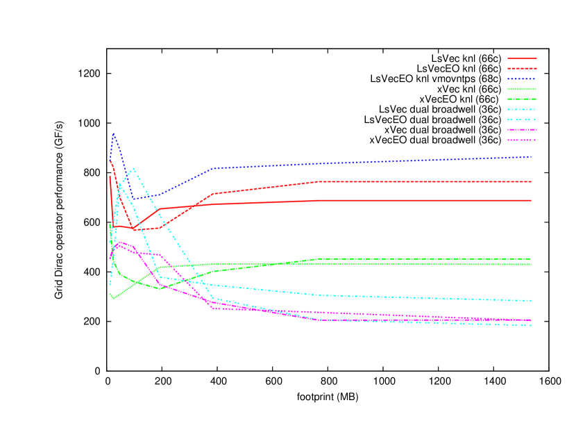
Grid has been particularly optimised for Knight’s Landing as part of an Intel Parallel Computing Centre at Edinburgh and Columbia, and the performance on a single KNL-7250 part is compared to that of two Cori Phase-1 Haswell chips as a function of the local volume in Figure 7 The team report multinode single precision performance at 400GF/s on a local volume on an Omnipath network when the job is spread out in four dimensions over nodes, after communications has been overlapped with computation.
One KNL was substantially faster than two Broadwell’s (18+18 cores) when the footprint was larger than cache due to the good performance of the high bandwidth on package memory. For comparison the thermal design power (TDP) for a dual Broadwell node is around 290W, while the TDP for a KNL node is around 210W, so that this increase in performance is accompanied by a reduction in power consumption. The Grid team report some other interesting metrics from performance measurements of their code:
-
•
not using all the cores was fastest; typically two spare cores help performance
-
•
best performance using inline assembly (not compiler intrinsics); this was due to the AVX512 instruction set having many registers and 3 operand instructions allowing hand allocation of registers to excel.
-
•
best performance was obtained with 1 thread per core on this highly optimised code; the L1 cache becomes a deterministic state machine only when a single thread runs, and stack evictions are eliminated since reused data is protected in registers.
-
•
Single core instructions-per-cycle is 1.7 from a possible 2.0.
-
•
Multi-core L1 hit rate was 99% due to perfect SFW prefetching
-
•
Multi-core MCDRAM read bandwidth saturated 97% of streams (370GB/s)
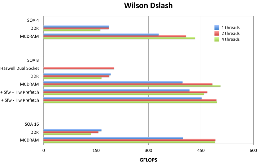
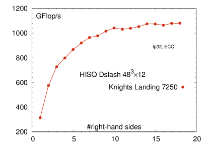
Wilson operator on KNL: The Intel and Jlab team developing QPhiX[17] have ported their code to KNL and provided both single node, Figure 7, and multinode performance benchmarks, Figure 8. These results are in single precision and make use of a single rail Omnipath 1.0 network. In contrast to the assembly programmed Grid benchmark, the intrinsics used rely on compiler register (non)allocation with the result that stack variables are (in practice) stochastically ejected from L1 cache by streaming data. A consequence of this is that best performance is obtained with several threads per core.
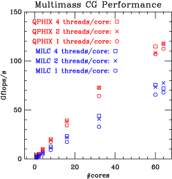
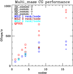
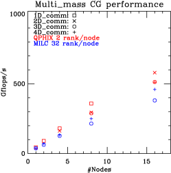
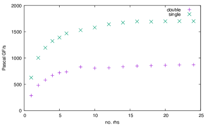
Staggered Fermion performance on KNL: The MILC multi-mass CG was presented by Ruizi Li, Figure 9 and Figure 10. This was based on a multimass solver in double precision and is heavily memory bandwidth limited. Indeed interconnection performance for this algorithm (depending on the number of masses, and the degree to which they converge after similar iteration counts) is somewhat irrelevant. In contrast, the multiple right hand side approach taken by Steinbrecher, Figure 10 is much more cache friendly and performs better. This latter approach is most useful for valence analysis. Steinbrecher’s code does not use MPI and is single node only, and is applied for trivially parallel disconnected diagram analyses. A multinode version of the same code would be rather more senstive to interconnect bandwidth than the benchmark discussed by MILC.
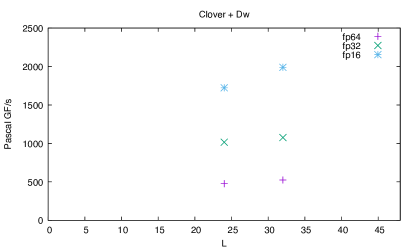
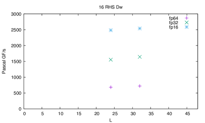
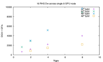
Nvidia Pascal Results: We focus first of all on results produced by Nvidia with the QUDA library. In these nodes a single GPU is capable of 5.4/10.6/21.2 TF/s in double/single/half precisions respectively. The Pascal results and code were provided by Kate Clark, Nvidia, and these comprise (a) the Wilson kernel and it cache friendly application to 5d chiral fermions (or multiple RHS solvers) Figure 11 and (b) the multiple right hand side improved Staggered fermion matrix and the scaling across an 8 GPU DGX-1 node Figure 12. In all cases the single node figures are roughly double a Kights Landing processor for single node execution, and this is consitent with the substantially improved HBM2 memory bandwidth compared to KNL. Multinode code will depend critically on the interconnect performance, and as indicated in Section 5 it is unlikely to be able to provision sufficient interconnect to produce a scalable system that does not have the local compute outstrip the network. It remains possible that multigrid algorithms with sufficiently aggressive domain decomposition preconditioners may scale. For conventional Krylov solvers, the ability of these nodes to scale across an MPI network is likely compromised, but at least for valence analysis multiple 10TF/s sustained nodes are not an unreasonable proposition. Unfortunately, the DGX-1 costs roughly $130,000 list price[20] or an eye watering $ 16,000 per GPU. The canny academic could no doubt maintain a fall back plan of using commodity parts and holding the pricing rather closer that of similar parts (e.g. Titan-X) sold to the volume gaming market. For example, an aggressive research group could tolerate less than 100% reliability by verfiying solutions to the Dirac equation with retry loop, or may even negotiate the better parts at a more reasonable price.
Offload to GPU poses difficulty to code maintainance and performance portability, and there has been a big community investment in QDP-JIT, for example, and vendor investment in architecture specific libraries such as QUDA. It was reported in this conference that the author and Meifeng Lin reduced the Grid expression template engine to 200 line-of-code example, and succeeded to offload with a CUDA kernel call to evaluate expression using “compile time compilation”, and specifically withour resorting to Just-In-Time compilation. This task will become even easier with unified memory model introduced with Pascal GPU’s.
James Osborn presented a package called “Quantum Expressions”, QEX, based on the “NIM” language[18]. The language, although not widespread or mature, has many attractive features and enables a controllable “nim to C” mapping. This in principle enables more flexible translation to GPU and indeed other targets, with more easily controllable mapping than is afforded by C++ template metaprogramming. Osborn believes this can generate equivalent or greater performance to C++ packages with greater flexibility and portability.
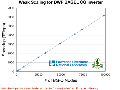
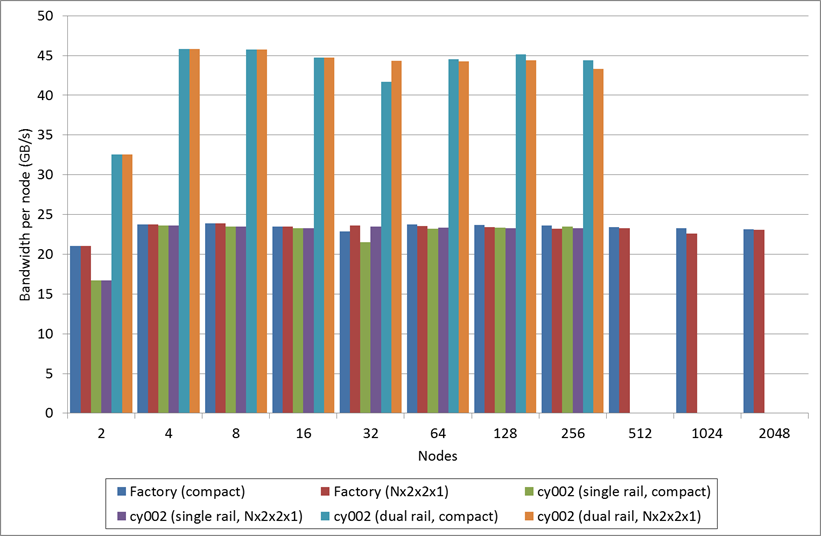
Communications performance results: As has been discussed, 5, performance in a massively parallel calculation is critically dependent on interconnect bandwidth. The Grid benchmark suite has been used to characterise many of the popular interconnects in forthcoming machines, Table 6. We see that compared to the BlueGene/Q 32 GB/s sustained bidirectional bandwidth in 2012, there is suprisingly little advance four years later[21]. With a 205GF/s peak node, the BlueGene/Q enable QCD scalability to 1.6 million cores, delivering 7.2 PF/s, Figure 13. This dwarves the figures of 10TF/s sustained scale figures beyond which we might fear that Dirac matrix applicatoin will not scale on a 8 GPU node. We can see that in principle we should seek to add network bandwidth in a way that scales with the node count, and hence the importance of integration of the interconnect. In this respect, the KNL-F design and the subsequent KNH remain interesting as our figures demonstrate the BlueGene/Q was scalable to system sizes beyond those the QCD community can actually afford.
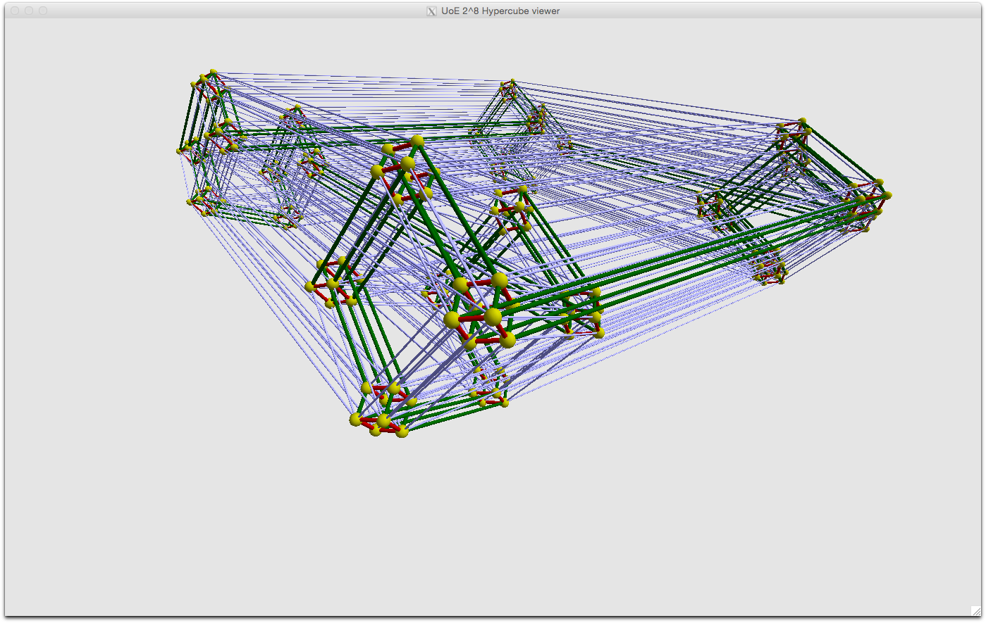
Since network becomes the large system performance limitation, we might seek to minimise network cost while maintaining peformance for QCD calculation. Both the QCDOC design[10], and subsequently QCD codes on the K-computer [24] and BlueGene/Q[21] have made use of precise mapping of the application logical 4d torus to underlying interconnect topologies. We present results provided by the Grid team in collaboration with Silicon Graphics, developing this theme on the ICE-X hypercube. SGI ran benchmarks on custom partitions of their machines with an exact power of two set of nodes on each switch (not the default) and demonstrated a 4x improvement in QCD scalability on 2048 node partitions. Further, when using the Mellanox EDR interconnect techonlogy, 80% of dual rail bidirectional bandwidth was obtained with no performance loss as weak scaled to any system size. This is a similar characteristic to the scaling of torus application codes on torii, although the job placement mapping was rather complex, Figure 13. With the correct MPI mapping, one can embed the QCD torus inside hypercube so that nearest neigbour comms travel only a single hop.
| Machine | Node | Network | 1 rank/node | 4 ranks/node | Peak | Require |
|---|---|---|---|---|---|---|
| Cori-1 | KNL | Cray Aries | 11 GB/s | - | - | 64 |
| SGI | KNL | Single EDR | 23 GB/s | - | 25GB/s | 64 |
| SGI | KNL | Dual EDR | 45 GB/s | - | 50GB/s | 64 |
| Brookhaven | KNL | Dual Omnipath | 14 GB/s | 44 GB/s | 50GB/s | 64 |
7 Algorithms
I have chosen to focus on two aspects that I feel are most fundamental to continued progress. These are multi-scale fermion solvers and block solvers, and multi-scale integration. I will not cover in detail, even though they are also fundamental, topological sampling (covered by Michael Endres’ review) and specifically metadynamics [25]. I pause only to comment on both that symptomatic relief is not necessarily a cure; We ideally want solutions that address all forms of critical slowing down in an exact MCMC chain that is run far enough to converge on the fixed point of the process. Fast thermalisation or creating a distaste for zero topological does not necessarily accelerate ergodic sampling of the fixed point distribution which might become slow even within a topological sector. I also do not review approaches to free energy, density of states and derived observables, as these were reviewed by Langfeld [26, 27, 28, 29].
Multiscale Fermion solvers: Several advances were reported in the area of Fermionic multigrid. Weinberg, Brower, Clark, Strelchenko reported on steps towards a multigrid solver for staggered fermions with demonstrated elimination of critical slowing down in two dimensional systems[22], Figure 14. Yamaguchi and Boyle[23] demonstrated the first solver and multigrid algorithm to work with 5D chiral fermions without squaring the operator, by using the hermitian operator. This is a key step to keep the compact radius of the coarse space operator limited and should enable a true, recursive multigrid. The authors claim to have understood the connection between the spectrum of the 5d operator and the constraints on which Krylov solvers work, and they hope that the nearest neighbour coarse space operator will be sufficiently cheap to recompute that the acceleration can be applied in HMC evolution.
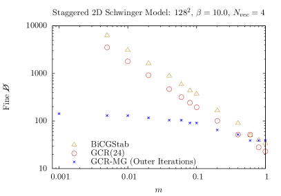
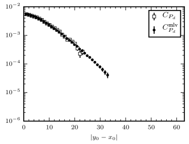
Stefan Schaefer and Marco Ce presented a promising quenched algorithm for multilevel integration[30]. By subdividing the lattice into disjoint regions with boundaries which are independently integrated over, they were able vastly improve the statistical samples by a factor where represents the samples drawn within each sub-region. For disconnected correlation functions this was demonstrated to give a substantial win, Figure 14. Further, elements of the DD-HMC determinant factorisation appear to be reusable making it fairly likely that these authors will be able to pursue this algorithm to a viable approach for dynamical fermions. Consequently, this is perhaps the uniquely most exciting algorithmic development of the conference. Further multigrid works include the development of a twisted mass multigrid, and the DD--AMG solver library [31]. The implementation of TWQCD’s Exact one flavour algorithm for DWF was discussed[32].
8 Summary
There has been a tremendous growth in computer power from many core CPU’s and GPU’s, with this years new products including Intel’s Knights Landing giving 0.5-1TF/s single node single precision sustained performance, and Nvidia’s Pascal giving 1-2 TF/s single node single precision sustained performance. However, interconnects are not keeping pace; this is disappointing since integration of interconnect in a manner that grows with the node transistor count should lead to scalable computing. The integration of interconnect on KNL-F and Skylake nodes is interesting but significant work may still be required to obtain scaling of QCD. The use of fp64/fp32/fp16 arithmetic in preconditioners or variance reduction is not yet fully explored, and could vastly both accelerate node computation, and in a network limited algorithm could be used in intelligent algorithms or rounding robust to minimise network overheads.
Multigrid solver algorithms have recently solved critical slowing down in valence sector for Wilson/Clover, and in this conference new multigrid algorithms have appeared for other actions (Staggered, DWF, Twisted Mass) Successful application of multigrid in HMC exists for Wilson/Clover, but is not yet widespread. Multilevel integration algorithms introduced in this conference are deeply interesting. Algorithms that maintain ergodicity are a big challenge to using this power usefully, but were reviewed elsewhere in the confernce.
Acknowledgements: The author is an Alan Turing Institute Faculty Fellow, acknowledges STFC grants ST/M006530/1, ST/L000458/1, ST/K005790/1, ST/K000411/1, ST/H008845/1, and ST/K005804/1, and Royal Society Wolfson Research Merit Award WM160035.
References
- [1] “Intel Xeon Phi(TM) Processor High Performance Programming, Knights Landing Edition, by Jim Jeffers, James Reinders, and Avinash Sodani.
- [2] https://images.nvidia.com/content/pdf/tesla/whitepaper/pascal-architecture-whitepaper.pdf
- [3] Shekhar Borkar, Andrew A. Chien, Communications of the ACM, Vol. 54 No. 5, Pages 67-77.
- [4] https://en.wikipedia.org/wiki/3D_XPoint
- [5] Wm. A. Wulf and Sally A. McKee. 1995. SIGARCH Comput. Archit. News 23, 1 (March 1995), 20-24.
- [6] Williams, S, Waterman, A and Patterson, D. Commun. ACM, April 2009, V52,4. PP65-76.
- [7] M Wagner, K. Clark, PoS Lattice 2016.
- [8] Computer Architecture: A Quantitative Approach, Hennessy and Patterson, Morgan Kaufmann.
- [9] F. T. Winter, M. A. Clark, R. G. Edwards and B. Joó, doi:10.1109/IPDPS.2014.112 arXiv:1408.5925 [hep-lat]. F. T. Winter, PoS LATTICE 2013 (2014) 042. F. Winter, arXiv:1111.5596 [hep-lat].
- [10] “Overview of the QCDSP and QCDOC computers”, IBM Journal of Research and Development ( Volume: 49, Issue: 2.3, March 2005 )
- [11] IBM Journal of Research and Development, Volume 57 Issue 1, January 2013
- [12] www.hotchips.org/wp-content/uploads/hc_archives/hc27/HC27.25-Tuesday-Epub/HC27.25.70-Processors-Epub/HC27.25.710-Knights-Landing-Sodani-Intel.pdf
- [13] P. A. Boyle, G. Cossu, A. Yamaguchi and A. Portelli, PoS LATTICE 2015 (2016) 023.
- [14] R. Babich, M. A. Clark and B. Joo, arXiv:1011.0024 [hep-lat].
- [15] C. DeTar, D. Doerfler, S. Gottlieb, A. Jha, D. Kalamkar, R. Li and D. Toussaint, arXiv:1611.00728 [hep-lat].
- [16] S. Mukherjee, O. Kaczmarek, C. Schmidt, P. Steinbrecher and M. Wagner, PoS LATTICE 2014 (2015) 044 [arXiv:1409.1510 [cs.DC]]. O. Kaczmarek, C. Schmidt, P. Steinbrecher and M. Wagner, doi:10.3204/DESY-PROC-2014-05/28 arXiv:1411.4439 [physics.comp-ph].
- [17] Lattice QCD on Intel Xeon Phi coprocessors. Balint Joo, Dhiraj D. Kalamkar, Karthikeyan Vaidyanathan, Mikhail Smelyanskiy, Kiran Pamnany, Victor W Lee, Pradeep Dubey, and William Watson III. In Proceedings of the 2013 International Supercomputing Conference, June 2013. Joo, Balint, et al. “Optimizing Wilson-Dirac Operator and Linear Solvers for Intel KNL.” International Conference on High Performance Computing. Springer International Publishing, 2016.
- [18] X. Y. Jin and J. C. Osborn, PoS ICHEP 2016 (2016) 187 [arXiv:1612.02750 [hep-lat]].
- [19] T. Boku, K. I. Ishikawa, Y. Kuramashi, L. Meadows, M. D‘Mello, M. Troute and R. Vemuri, “A performance evaluation of CCS QCD Benchmark on the COMA (Intel(R) Xeon Phi, KNC) system,” PoS LATTICE 2016 261 [arXiv:1612.06556 [hep-lat]].
- [20] https://www.nextplatform.com/2016/04/06/dgx-1-nvidias-deep-learning-system-newbies/
- [21] “The BlueGene/Q supercomputer” P.A. Boyle (Edinburgh U.) PoS LATTICE2012 (2012) 020
- [22] E. Weinberg, R. Brower, K. Clark, A. Strelchenko, “Staggered Multigrid” PoS Lattice 2016.
- [23] A. Yamaguchi and P. Boyle, “Hierarchically deflated conjugate residual,” arXiv:1611.06944 [hep-lat].
- [24] Y. Ajima, S. Sumimoto and T. Shimizu, “Tofu: A 6D Mesh/Torus Inter-connect for Exascale Computers,” IEEE Computer, vol. 42, no. 11, pp. 36-40, 2009.
- [25] A. Laio, G. Martinelli and F. Sanfilippo, “Metadynamics surfing on topology barriers: the case,” JHEP 1607 (2016) 089
- [26] K. Langfeld, “Density-of-states,” arXiv:1610.09856 [hep-lat].
- [27] A. Nada, M. Caselle, G. Costagliola, M. Panero and A. Toniato, “Applications of Jarzynski’s relation in lattice gauge theories,” arXiv:1610.09017 [hep-lat].
- [28] “Computing the density of states with the global Hybrid Monte Carlo”, R. Pellegrine, V. Davide, B. Lucini, and A. Rago. PoS Lattice 2016.
- [29] B. Lucini, W. Fall and K. Langfeld, “Overcoming strong metastabilities with the LLR method,” arXiv:1611.00019 [hep-lat].
- [30] M. Ce, L. Giusti and S. Schaefer, arXiv:1612.06424 [hep-lat]. M. Ce, L. Giusti and S. Schaefer, arXiv:1609.02419 [hep-lat]. M. Ce, L. Giusti and S. Schaefer, Phys. Rev. D 93 (2016) no.9, 094507
- [31] S. Bacchio, C. Alexandrou, J. Finkenrath, A. Frommer, K. Kahl and M. Rottmann, arXiv:1611.01034 [hep-lat]. C. Alexandrou, S. Bacchio, J. Finkenrath, A. Frommer, K. Kahl and M. Rottmann, Phys. Rev. D 94 (2016) no.11, 114509
- [32] “Domain Wall Fermion Simulations with the Exact One-Flavor Algorithm”, D. Murphy, PoS Lattice 2016.