Thermal resistance of grain boundaries in silicon nanowires by nonequilibrium molecular dynamics
Abstract
The thermal boundary resistance (Kapitza resistance) of (001) twist grain boundaries in silicon nanowires depends on the mismatch angle. This dependence is systematically investigated by means of nonequilibrium molecular dynamics simulations. Grain boundary systems with and without coincidence site lattice are compared. The Kapitza resistance increases with twist angle up to . For larger angles, it varies only little around , except for a drop by near the grain boundary. Finite size effects due to the fixed outer boundary conditions of the nanowire are negligible for diameters larger than .
I Introduction
Due to its thermal and electronic transport properties, it is a promising approach to use nanostructured silicon as thermoelectric material.Schierning (2014) The efficiency of a thermoelectric device at temperature increases with the material’s figure of merit ,
| (1) |
where is the Seebeck coefficient, the electrical conductivity, and the thermal conductivity. As consists only of material properties, target-oriented material design is the consequent approach to improve the efficiency of thermoelectric generators.
Evidently, it is desirable to find materials with a high Seebeck coefficient, a high electrical conductivity, and a low thermal conductivity. The approach in this work is to reduce the phononic contribution to heat conduction without significantly decreasing the electronic transport. This is possible in crystalline silicon, because of the thermal transport is carried by phonons with mean free paths of and longer.Regner et al. (2013) Electrons, on the other hand, have effective mean free paths on a much shorter scale.Schierning (2014) Due to advances in processing, highly doped polycrystalline silicon with crystallite sizes in the order of can be prepared from nanoparticles.Schierning et al. (2011) For structures on the nano scale, the phonon scattering is expected to change, making phonon-surface scattering the most important mechanism.Schierning (2014) The expected significant reduction in thermal conductivity was achieved by producing silicon materials consisting of nanosized crystalline grains.Schierning et al. (2011)
While the thermal conductance, and thus the average influence of grain boundaries (GBs) in polycrystalline silicon films, was measured experimentally,Uma et al. (2001) the investigation of actual individual grain boundaries is challenging. Therefore, molecular dynamics (MD) simulations can be of great help to elucidate transport processes and estimate the magnitude and behavior of thermal material properties.Maiti, Mahan, and Pantelides (1997); Schelling, Phillpot, and Keblinski (2002, 2004); Kimmer et al. (2007); Watanabe et al. (2007); da Cruz et al. (2011)
Mainly, we will investigate the dependence of thermal resistance at twist grain boundaries on the twist angle. Based on results of former MD simulations for silicon and diamond grain boundaries,Schelling, Phillpot, and Keblinski (2004); Watanabe et al. (2007); Ju and Liang (2013) we expect interfacial resistances in the order of a few and an increase with twist angle up to at least . Using systems of finite size with fixed boundary conditions, we also aim at simulating the thermal processes between two actual grains of a given size more accurately as for periodic boundary conditions. On the other hand, we will need to estimate inadequacies due to the artificial fixed atomistic walls.
II Methods
Thermal transport in silicon is simulated by nonequilibrium molecular dynamics (NEMD) using the Stillinger-Weber potential with original parameters,Stillinger and Weber (1985) which is well characterized and was shown to produce realistic results in previous cases. Schelling, Phillpot, and Keblinski (2004); Wang et al. (2009); da Cruz et al. (2011); Ju and Liang (2013) For our simulations, we used the well established program LAMMPS.Plimpton (1995)
To obtain rotationial symmetry, we choose cylindrical geometry for the investigated nanowires, as shown in Fig. 1. The fixed atomistic walls have a thickness of lattice constants for the cylindrical shell and one lattice constant at both ends. Both the mobile part and the fixed walls consist of isotopically pure . Particle-wall interactions are described by the same potential as particle-particle interactions.
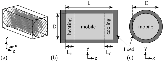
The following method is used to establish a constant one dimensional heat flux through the system (along ): A slab of the nanowire (thickness ) at one end is heated by adding a certain amount of kinetic energy per time step to the atoms by rescaling their velocity vectors accordingly. The slab at the other end (thickness ) is cooled by the same method, extracting the same amount of kinetic energy per time step and thus maintaining energy conservation of the whole system. The heating and cooling regions are scaled with the system length having always a thickness of .
In stationary state, the heat flux density is homogeneous and amounts to
| (2) |
where is the cross sectional area of the cylindrical nanowire.
The local instantaneous temperature is defined by dividing the wire into slabs (with thickness of one lattice constant ) and respectively averaging the kinetic energy of the contained inner degrees of freedom at a given time step,
| (3) |
where is the Boltzmann constant. This instantaneous temperature is then averaged over a time interval to produce a temperature profile , which, in the stationary state, does not depend on time except for statistical fluctuations.
Initially, the atoms are placed at the equilibrium positions of the silicon lattice and are given random velocities corresponding to a Maxwell-Boltzmann distribution with a temperature of . Thereafter, the MD simulation with a time step of consists of two phases: First, the system is equilibrated for at using the Nosé-Hoover-thermostatNosé (1984) with constant volume and constant number of particles (-ensemble). For large systems ( or ) this equilibration time is extended to . Second, the heat flux is established and maintained for . In this second phase, the system is given a time of to reach the stationary state and the last are used to measure and average the temperature profiles. The heat flux density is chosen to be the same for all investigated systems ().
II.1 Measuring thermal conductivity
At first, we investigate the thermal properties of crystalline nanowires devoid of any grain boundary (GB). Knowing the heat flux and the temperature profile from the simulation, the thermal conductivity is determined from Fourier’s law (in one dimension):
| (4) |
If Fourier’s law is valid and is constant, we expect a linear temperature profile, provided does not vary too much spatially. Figure 2 shows that linearity is given in the middle of the nanowire. At the ends, where the heating and cooling takes place, the system is not in local equilibrium and Fourier’s law does not apply. In the heat source and sink, the system is externally perturbed by rescaling the velocities and can not reach local equilibrium, which also influences the adjacent regions. The nonlinear behavior was reported by other authors,Schelling, Phillpot, and Keblinski (2002); da Cruz et al. (2011) and accounted for by the modified phonon scattering at the heating and cooling regions.
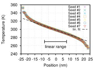
Therefore, the profiles are fitted in the linear range and is calculated from Eq. (4). To proof consistency, we simulate the same system several times, only changing the seed of the random number generator that creates the initial velocity distribution. Although the different profiles in Fig. 2 do not vary much in the graphical representation, numerical evaluation shows that the thermal conductivities vary about 1%.
To account for these statistical variations, we average the temperature profiles of the different seeds, which leads to a mean profile with error bars. The slope in the linear range and its uncertainty are then determined from the mean profile and its error bars.
II.2 Grain boundaries and Kapitza resistance
To implement a twist grain boundary of a certain angle, one half of the cylindrical mono-crystalline nanowire is rotated with respect to the other, including the fixed walls, by a twist angle , as can be seen in Fig. 3. The rotation plane (x-y) is an (001)-plane of the diamond lattice. This prescribes the initial atom configuration. We simulate GB systems with and without a coincidence site lattice (CSL).Santoro and Mighell (1973) The former are called grain boundaries. corresponds to the size of the primitive unit cell of the CSL relative to the original primitive unit cell of silicon.
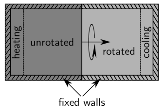
We choose fixed boundary conditions, because we want to be able to investigate finite size effects and arbitrary grain boundary twist angles. For periodic boundary conditions, only some specific angles, which create a coincidence site lattice, would be possible to simulate.Schelling, Phillpot, and Keblinski (2004) Furthermore, rotation symmetry is necessary for fixed boundary conditions to obtain equivalent regions on both sides of the grain boundary planes. This, in the end, is the reason for using systems with cylindrical geometry.
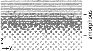
During the thermostat phase, an amorphous region emerges at the grain boundary. Common neighbor analysis, as proposed by Honeycutt and Andersen,Honeycutt and Andemen (1987) shows, which atoms are considered to be in an crystalline environment of the diamond lattice and which have no crystalline order (see Fig. 4). The thickness of the amorphous region is estimated and lies between one and three lattice constants, depending on the twist angle and system dimensions.
The grain boundaries constitute a resistance to thermal transport, called Kapitza resistance . In the presence of a heat flux, it leads to a temperature discontinuity at the interface,
| (5) |
which is visible in the simulated profiles (see Fig. 5).
The temperature jump is determined by extrapolating the linear ranges on both sides of the grain boundary and taking the difference of the linear fits at the interface (see Fig. 5). Knowing the constant heat flux density, the Kapitza resistance is then calculated using Eq. (5).
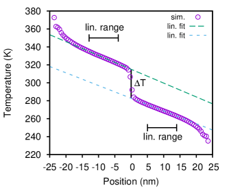
Again, the consistency of the results is checked by comparing simulation runs with different initial velocity distributions. Although the graphical representation shows no major visible differences of the temperature profiles (see Fig. 6), the numerical evaluation of the temperature gap leads to significant deviations between the runs. Therefore the profiles are averaged, as for the GB-free systems (cf. Sec. II.1), to create a mean profile with statistical error bars for each data point. The Kapitza resistance and its uncertainty are determined from the linear fits to this mean profile.

III Results and discussion
In this section, we analyze finite size effects on the thermal properties of systems with and without grain boundary to discuss the influence of the chosen geometry and fixed boundary conditions. We then present our results of the Kapitza resistance measurements for GB systems with 33 different twist angles.
III.1 Finite size effects on the thermal conductivity
The mono-crystalline, cylindrical system is simulated for four different wire lengths from to with a constant diameter of . Figure 7 shows that the thermal conductivity increases with length and (for our system) lies between and . Schelling et al. reported a similar behavior (increase of with system length) for periodic boundary conditions due to the reduction of the phonon mean free path.

Likewise, we vary the diameter six times between and for a constant length of to investigate the influence of the cross section. As can be seen in Fig. 8, the thermal conductivity also increases with diameter and attains values between and . However, the system length’s influence on the heat conduction is much stronger than the diameter’s.

It is well known from experiment and simulation that heat conduction is reduced in nano-sized and nano-crystalline media.Schelling, Phillpot, and Keblinski (2002); Li et al. (2003); da Cruz et al. (2011) By comparing our results to experimental values of for bulk Capinski et al. (1997), we can confirm a reduction of the thermal conductivity in nanowires by one to two orders of magnitude.
Da Cruz et al.da Cruz et al. (2011) used NEMD to study the thermal transport in nanowires of square cross section for different potentials and boundary conditions. They reported similar finite size effects, i.e., increase of the thermal conductivity with length and cross sectional area . For fixed atomistic boundary conditions and and the Stillinger-Weber potential, they measured for a length of and cross section of .
For a further investigation and comparison, we simulate a nanowire with square cross section of and , leading to . Extrapolating to the dimensions used by da Cruz et al. (stated above), we obtain , which is in good agreement with their result of .
Comparing the cuboidal setup with our cylindrical system of same length and cross sectional area, i.e. and , we note a reduction in the thermal conductivity to . Thus, by solely changing the shape of the cross section from square to circular, the heat conduction is reduced by . We attribute this to inadequacies of the MD simulation, especially in combination with fixed boundary conditions:
For the square cross section, the mobile part of the system consists of entire cubic unit cells. For the cylindrical geometry the unit cells near the walls will be cut into regions of mobile and fixed atoms. We propose that the reduction in thermal conductivity is a consequence of the less regular and less periodic particle-wall bonds, which introduce additional phonon scattering. Additionally, da Cruz et al.da Cruz et al. (2011) observed that, for simulated nanowires, the thermal conductivity is about twice as high for fixed boundary conditions as for free boundary conditions in the transversal (x-y) directions.
Due to the challenge of characterizing nano scale systems experimentally and the imperfect material properties, comparison with real systems is difficult. Li et al.Li et al. (2003) investigated isotopically natural, intrinsic, crystalline Si nanowires with diameters of and a length of several microns, measuring thermal conductivities of about at . Moreover, the results of Boukai et al.Boukai et al. (2008) indicated experimental values of about for highly doped Si nanowires with cross sectional areas of , and of roughly for . Here, the wires were also several microns long.
We compare those values with for our largest simulated diameter of (and ). Based on the preceding considerations, we conclude an overestimation of the heat conduction in our simulated systems compared to natural and doped Si nanowires. Reasons are the artificial fixed boundary conditions, the isotopic purity, the perfection of the crystal lattice and material surface without impurities or oxidation, and, most importantly for small systems, the disregard of quantum mechanical effects, which will lead to significant variations, even for a temperature of .Wang et al. (2009)
Nevertheless, NEMD can give important information for thermal processes under perfect conditions and indications of the thermal properties. Moreover, it is most useful to investigate the influence of parameter variations by tendency, like scaling dimensions, or, in our case, varying the grain boundary twist angle (see Sec. III.3).
III.2 Finite size effects on the Kapitza resistance
Next, we present our results for the simulated grain boundary systems, investigating the influence of length, diameter, and, in Sec. III.3, twist angle variations on the thermal boundary resistance. The GB system with is simulated for five different lengths from to , leading to a Kapitza resistance in the range from to (see Fig. 9). Although the shortest and longest system have the highest and lowest resistance, respectively, we can not conclude a systematic trend in the light of the given uncertainties. In fact, except for the highest value, the deviation from the mean is covered by the error bars and the highest deviation amounts to (see Fig. 9). While we can not exclude a possible influence of the system length on the Kapitza resistance, the results state at any rate that it is of minor importance for the considered dimensions. Schelling et al.Schelling, Phillpot, and Keblinski (2004) used NEMD with periodic boundary conditions to study heat conduction in Si grain boundaries. They also report very little effect of length variations on the Kapitza resistance for the (001) GB system.

A Variation of the diameter, on the other hand, leads to a strong and systematic behavior of the Kapitza resistance. For the same twist angle of and a constant length of , we use five different diameters from to . As can be seen in Fig. 10, the Kapitza resistance shows a decreasing and converging trend with increasing cross sectional area. Plotting versus inverse squared diameter leads to data that is in good agreement with a linear fit. Although we did not establish a theory to explain this behavior, we justify the approach
| (6) |
with , and a coefficient , by the high quality of the fit.

Furthermore, we extrapolate to infinite cross sectional area () to investigate the influence of the fixed boundary conditions. Our argument is that for , all types of lateral boundary conditions (free, fixed, and periodic in x-y-directions) should converge to the same results. From the extrapolation, we can estimate how big the modification due to the fixed boundaries can be at the most. Table 1 shows that the deviation of the Kapitza resistance from is and less for diameters of . We propose that for larger diameters, the differences in caused by different lateral boundary conditions should become sufficiently small.
| 0.29 | |||
| 0.17 | |||
| 0.08 | |||
| 0.05 | |||
| 0.03 |
However, due to the high computational effort for large systems, we use and to investigate the twist angle’s influence in Sec. III.3. If necessary, we are then able to extrapolate to infinite cross section by reducing the boundary resistance by about . The finite size analysis was done only for the presented GB. Nevertheless, we expect similar behavior for other twist angles, and use the same scaling law as a first approach.
III.3 Dependence of Kapitza resistance on the grain boundary angle
We investigate 25 twist angles from to in equal steps of . Due to the twofold symmetry of the diamond lattice, angles of have equivalent configurations and should lead to the same results. This is verified for our simulations by comparing the and angle systems, which indeed yield the same Kapitza resistance of (see Fig. 11).

Additionally, we simulate eight GB systems with coincidence site lattices. Here, the five smallest values are chosen for investigation. Thus, including the GB, we study nine grain boundaries (see Table 2) and a total of 33 GB systems. The determined values of the thermal boundary resistance for all angles are summarized in Table 3.
| 25 | 16.26 | 73.74 |
|---|---|---|
| 13 | 22.62 | 67.38 |
| 17 | 28.07 | 61.93 |
| 5 | 36.87 | 53.13 |
| 1 | (0.00) | 90.00 |
Within the error bars, Fig. 11 shows a monotonous increase of the Kapitza resistance with twist angle up to . For larger angles, i.e., from to , is nearly constant with fluctuations about a mean of approximately , as can also be seen in more detail in Fig. 12. We note a drop in of about for the special GB at . Besides this case, based on our results, we can not state with certainty that grain boundaries have distinguished heat conduction properties compared to grain boundaries with similar angles. While the GB seems to constitute a local maximum in thermal boundary resistance, this could easily be caused by statistical uncertainties or simulation inaccuracies, considering the magnitude of the error bars (see Fig. 12). The same applies to the local minima at some of the other angles (, , and ). Although it is reasonable to assume modified heat conduction in CSLs due to the increased periodicity of the superlattice, we can not confirm this behavior. The effect of enhanced periodicity might be suppressed by the finite thickness of the amorphous region and the size of the sectional area not being big enough to contain many CSL unit cells.

Schelling et al.Schelling, Phillpot, and Keblinski (2004) used a method similar to ours, but with periodic boundary conditions, to simulate (001) Si twist grain boundaries for angles of , and . Their results indicate Kapitza resistances of , and , respectively, for . From theory and further simulations, the thermal boundary resistance is expected to increase for lower temperatures.Kimmer et al. (2007); Aubry et al. (2008) In an estimation, based on results regarding temperature dependency by Aubry et al.Aubry et al. (2008), we assume that the values of should increase by about to , when the temperature decreases from to . Our closest angles for comparison are , and . Based on the finite size analysis in Sec. III.2, we furthermore reduce our values by , which leads to , and , respectively. Under the preceding considerations, our values agree well with those of Schelling et al.Schelling, Phillpot, and Keblinski (2004), stated above.
Ju and LiangJu and Liang (2013) studied (001) Si twist grain boundaries by NEMD simulation with periodic boundary conditions for different temperatures. Their results for indicate Kapitza resistances of about , and for angles of , and , respectively. If we extrapolate our results for these angles from Table 3 to infinite cross section, our values for reach only about of Ju and Liang’s. The deviations might arise due to different methods used during the equilibration of the grain boundaries prior to the heat flux phase. While we use a -thermostat for our fixed boundary conditions, they use a -thermostatNosé (1984) (with constant pressure ) to relax the system with periodic boundary conditions. Consequently, in our system, we expect both the pressure to be higher and a modified structure of the grain boundary in the vicinity of the fixed walls. However, the differences caused by different configurations should diminish with increasing cross sectional area. Another reason for the deviation of the results might be differences in the heat flux generation, as they use the Müller-Plathe method,Müller-Plathe (1997) while we use velocity rescaling. Nevertheless, the values of are in the same order of magnitude and our simulations yields reasonable information on the grain boundary angle’s influence on thermal boundary resistance.
IV Conclusion
We used NEMD to study thermal transport in crystalline nanowires with and without (001) twist grain boundaries. A cylindrical geometry was necessary for GB systems with fixed boundary conditions. Dimensions were in the range of and . The fixed boundary conditions led to significant finite size effects. The thermal conductivity increased with both length and diameter, where the former had a much stronger influence (see Figs. 7 and 8). The shortest investigated system yielded a thermal conductivity of about , which agrees well with results of da Cruz et al.da Cruz et al. (2011). Increasing this system length eightfold increased by a factor of . The basic configuration for the grain boundary analysis had dimensions of , and , yielding . Compared to experimental values for crystalline bulk , the thermal conductivity has been reduced by one order of magnitudeCapinski et al. (1997).
Concerning the thermal Kapitza boundary resistance, we noted very little effect due to length variations (see Fig. 9). In contrast, the Kapitza resistance decreased clearly and systematically with cross sectional area. Our results indicate a linear drop with inverse cross section (see Fig. 10). We used this approach to extrapolate to infinite cross section, for which the influence of the artificial fixed boundary conditions should vanish. For the GB with basic dimensions, this implied an overestimation of by about , compared to infinite cross section. The Kapitza resistance converged quite quickly with diameter, i.e., already for (approx. ) the deviation from the extrapolation to infinite cross section was reduced to . Increasing further to decreased the deviation to . For future simulations with fixed boundary conditions, we suggest to use diameters of at least this magnitude.
Heat conduction was simulated for 33 different (001) twist grain boundaries from to (see Fig. 11). Up to , the Kapitza resistance increased with twist angle. For angles from to , we could not detect systematic behavior (see Fig. 12). The values of remained rather constant, fluctuating between and . Compared to this range, the thermal boundary resistance dropped sharply by for the GB system. In the context of the calculated uncertainties, we can neither state nor deny distinguished thermal properties of the other CSL grain boundaries compared to adjacent angles. It would be desirable to simulate GB systems with larger diameter for more angles. In doing so, it could be analyzed whether a special behavior of systems is prevented by cross sections which are to small to contain enough CSL unit cells.
Compared to periodic boundary conditions, we hoped to reproduce more accurately the thermal processes between individual nano particles with finite dimensions. It would be enlightening to investigate whether any major shortcomings arise due to the used artificial fixed boundary conditions. This could best be done by comparing to further simulations with free boundary conditions. Because our extrapolated values of the Kapitza resistance agree well with those of Schelling et al.,Schelling, Phillpot, and Keblinski (2004) we are confident that our measured values are in a realistic range (cf. Sec. III.3). At any rate, our results yield information on the twist angle’s qualitative influence on thermal boundary resistance. Concerning heat conduction in thermoelectric materials composed of nano particles, we conclude that the relative orientation of the grains should be of importance. Increasing the number of high angle grain boundaries in polycrystalline material should reduce thermal conductance of the entire system.
Acknowledgements.
This research has been supported by the German Research Foundation (DFG) (grant no. WO577/10-1 and WO577/6-2) within the priority program SPP 1386 Nanostructured Thermoelectric Materials: Theory, Model Systems and Controlled Synthesis.References
- Schierning (2014) G. Schierning, Physica Status Solidi (a) 15, 1235 (2014).
- Regner et al. (2013) K. T. Regner, D. P. Sellan, Z. Su, C. H. Amon, A. J. H. McGaughey, and J. Malen, Nature communications 4, 1640 (2013).
- Schierning et al. (2011) G. Schierning, R. Theissmann, N. Stein, N. Petermann, A. Becker, M. Engenhorst, V. Kessler, M. Geller, A. Beckel, H. Wiggers, and R. Schmechel, Journal of Applied Physics 110, 113515 (2011).
- Uma et al. (2001) S. Uma, A. D. McConnell, M. Asheghi, K. Kurabayashi, and K. E. Goodson, International Journal of Thermophysics 22, 605 (2001).
- Maiti, Mahan, and Pantelides (1997) A. Maiti, G. D. Mahan, and S. T. Pantelides, Solid State Communications 102, 517 (1997).
- Schelling, Phillpot, and Keblinski (2002) P. K. Schelling, S. R. Phillpot, and P. Keblinski, Physical Review B 65, 144306 (2002).
- Schelling, Phillpot, and Keblinski (2004) P. K. Schelling, S. R. Phillpot, and P. Keblinski, Journal of Applied Physics 95, 6082 (2004).
- Kimmer et al. (2007) C. Kimmer, S. Aubry, A. Skye, and P. K. Schelling, Physical Review B - Condensed Matter and Materials Physics 75, 144105 (2007).
- Watanabe et al. (2007) T. Watanabe, B. Ni, S. R. Phillpot, P. K. Schelling, and P. Keblinski, Journal of Applied Physics 102, 063503 (2007).
- da Cruz et al. (2011) C. A. da Cruz, K. Termentzidis, P. Chantrenne, and X. Kleber, Journal of Applied Physics 110, 034309 (2011).
- Ju and Liang (2013) S. H. Ju and X. G. Liang, Journal of Applied Physics 113, 053513 (2013).
- Stillinger and Weber (1985) F. H. Stillinger and T. A. Weber, Physical Review B 31, 5262 (1985).
- Wang et al. (2009) S.-C. Wang, X.-G. Liang, X.-H. Xu, and T. Ohara, Journal of Applied Physics 105, 014316 (2009).
- Plimpton (1995) S. Plimpton, Journal of Computational Physics 117, 1 (1995).
- Nosé (1984) S. Nosé, Mol. Phys. 52, 255 (1984).
- Santoro and Mighell (1973) A. Santoro and A. D. Mighell, Acta Crystallographica Section A 29, 169 (1973).
- Honeycutt and Andemen (1987) J. D. Honeycutt and H. C. Andemen, Journal of Physical Chemistry 91, 4950 (1987).
- Li et al. (2003) D. Li, Y. Wu, P. Kim, L. Shi, P. Yang, and A. Majumdar, Applied Physics Letters 83, 2934 (2003).
- Capinski et al. (1997) W. S. Capinski, H. J. Maris, E. Bauser, I. Silier, M. Asen-Palmer, T. Ruf, M. Cardona, and E. Gmelin, Applied Physics Letters 71, 2109 (1997).
- Boukai et al. (2008) A. I. Boukai, Y. Bunimovich, J. Tahir-Kheli, J.-K. Yu, W. A. Goddard, and J. R. Heath, Nature 451, 168 (2008).
- Aubry et al. (2008) S. Aubry, C. J. Kimmer, A. Skye, and P. K. Schelling, Physical Review B - Condensed Matter and Materials Physics 78, 064112 (2008).
- Müller-Plathe (1997) F. Müller-Plathe, The Journal of Chemical Physics 106, 6082 (1997).