Conductance through a helical state in an InSb nanowire
The motion of an electron and its spin are generally not coupled. However in a one dimensional (1D) material with strong spin-orbit interaction (SOI) a helical state may emerge at finite magnetic fields,Streda2003 ; Pershin2004 where electrons of opposite spin will have opposite momentum. The existence of this helical state has applications for spin filtering and Cooper pair splitter devicesSato2010 ; Rashba2016 and is an essential ingredient for realizing topologically protected quantum computing using Majorana zero modes.alicea2011 ; Nayak2008 ; Yuval2010 Here we report electrical conductance measurements of a quantum point contact (QPC) formed in an indium antimonide (InSb) nanowire as a function of magnetic field. At magnetic fields exceeding , the plateau shows a reentrant conductance feature towards which increases linearly in width with magnetic field before enveloping the plateau. Rotating the external magnetic field either parallel or perpendicular to the spin orbit field allows us to clearly attribute this experimental signature to SOI. We compare our observations with a model of a QPC incorporating SOI and extract a spin orbit energy of , which is significantly stronger than the SO energy obtained by other methods.
Spin-orbit interaction is a relativistic effect where a charged particle moving in an electric field with momentum and velocity , experiences an effective magnetic field in its rest frame. The magnetic moment of the electron spin, , interacts with this effective magnetic field, resulting in a spin-orbit Hamiltonian that couples the spin to the orbital motion and electric field. In crystalline materials, the electric field arises from a symmetry breaking that is either intrinsic to the underlying crystal lattice in which the carriers move, known as the Dresselhaus SOI,dresselhaus1955 or an artificially induced asymmetry in the confinement potential due to an applied electric field, or Rashba SOI.rashba2015 Wurtzite and certain zincblende nanowires possess a finite Dresselhaus SOI, and so the SOI is a combination of both the Rashba and Dresselhaus components. For zincblende nanowires grown along the [111] growth direction the crystal lattice is inversion symmetric, and so only a Rashba component to the spin-orbit interaction is thought to remain.winkler2003
Helical states have been shown to emerge in the edge mode of 2D quantum spin hall topological insulators,Koenig2007 ; nowack2013 and in quantum wires created in GaAs cleaved edge overgrowth samples.quay2010 They have also been predicted to exist in carbon nanotubes under a strong applied electric field,klinovaja2011 RKKY systems,klinovaja2013topological and in InAs and InSb semiconducting nanowires where they are essential for the formation of Majorana zero modes. Although the signatures of Majoranas have been observed in nanowire-superconductor hybrid devices,mourik2012signatures ; albrecht2016exponential explicit demonstration of the helical state in these nanowires has remained elusive. The measurement is expected to show a distinct experimental signature of the helical state - a return to conductance at the plateau in increasing magnetic field as different portions of the band dispersion are probed.Streda2003 ; Pershin2004 ; Rainis2014 While ballistic transport through nanowire QPCs is now standard,kammhuber2016conductance ; heedt2016ballistic numerical simulations have shown that the visibility of this experimental signature critically depends on the exact combination of geometrical and physical device parameters.Rainis2014
Here we observe a clear signature of transport through a helical state in a QPC formed in an InSb nanowire when the magnetic field has a component perpendicular to the spin-orbit field. We show that the state evolves under rotation of the external magnetic field, disappearing when the magnetic field is aligned with . By comparing our data to a theoretical model, we extract a spin orbit energy , significantly stronger than that measured in InSb nanowires by other techniques.
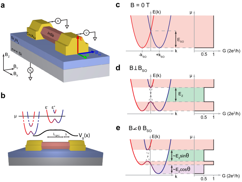
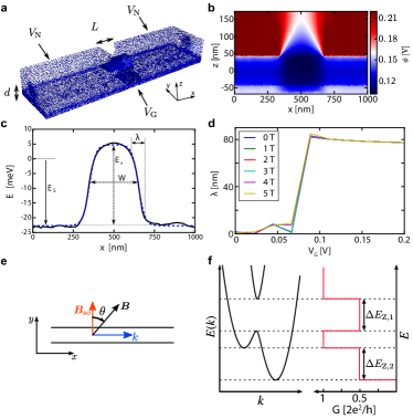
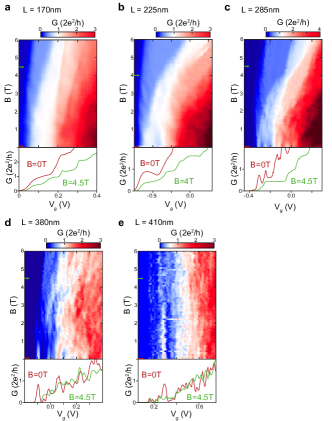
Figure 1a shows a schematic image of a typical QPC device. An InSb nanowire is deposited on a degenerately doped silicon wafer covered with a thin () SiN dielectric. The QPC is formed in the nanowire channel in a region defined by the source and drain contacts spaced apart. The chemical potential in the QPC channel, which sets the subband occupation, is controlled by applying a voltage to the gate . The electric field in the nanowire, , generated by the backgate and the substrate that the nanowire lies on, both induce a structural inversion asymmetry that results in a finite Rashba spin orbit field. As the wire is translationally invariant along its length, the spin orbit field, , is perpendicular to both the electric field and the wire axis. The effective channel length, , as well as the shape of the onset potential are set by electrostatics which are influenced by both the thickness of the dielectric and the amount of electric field screening provided by the metallic contacts to the nanowire (Fig 1b). Here we report measurements from one device. Data from an additional device that shows the same effect, as well as control devices of different channel lengths and onset potentials, is provided in the Supplementary Information.
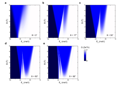
The energy-momentum diagrams in Fig 1c-e show the dispersion from the 1D nanowire model of Refs. 1 and 2 including both SOI with strength and Zeeman splitting , where is the -factor, the Bohr magneton and the magnetic field strength. These dispersion relations explain how the helical gap can be detected: Without magnetic field, the SOI causes the first two spin degenerate sub-bands to be shifted laterally in momentum space by with the effective electron mass, as electrons with opposite spins carry opposite momentum, as shown in Fig 1c. The corresponding spin-orbit energy is given by . However, here Kramers degeneracy is preserved and hence the plateaus in conductance occur at integer values of , as for a system without SOI. Applying a magnetic field perpendicular to BSO the spin bands hybridize and a helical gap, of size opens as shown in Fig 1d. When the chemical potential is tuned by the external gate voltage, it first aligns with the bottom of both bands resulting in conductance at before reducing from to when is positioned inside the gap. This conductance reduction with a width scaling linearly with increasing Zeeman energy, is a hallmark of transport through a helical state. When the magnetic field is orientated at an angle to , the size of the helical gap decreases as it is governed by the component of the magnetic field perpendicular to , as shown in Fig 1e. Additionally, the two sub-band bottoms also experience a spin splitting giving rise to an additional Zeeman gap. For a general angle , the QPC conductance thus first rises from 0 to , then to , before dropping to again. The helical gap thus takes the form of a re-entrant conductance feature. By comparing to a 1D nanowire model, we can extract both the size of the helical gap and the Zeeman shift (see Supplementary Information). This angle dependency is a unique feature of SOI and can be used as a decisive test for its presence in the experimental data.
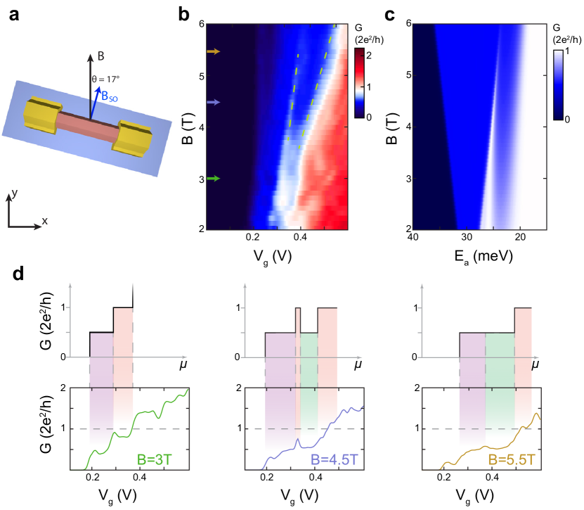
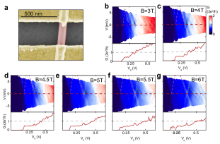
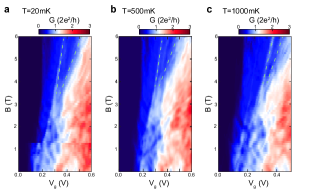
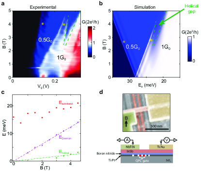
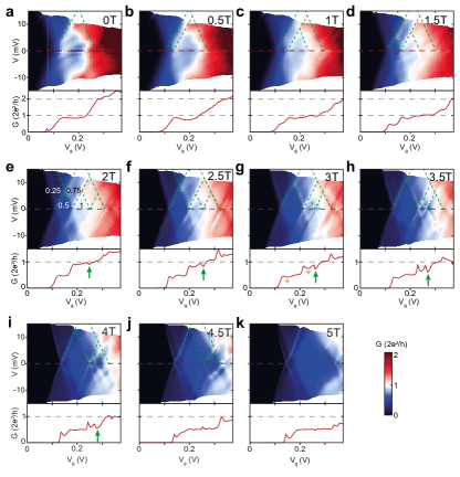
Figure 2 shows the differential conductance of our device at zero source-drain bias as a function of gate and magnetic field. Here the magnetic field is offset at a small angle from (see Fig 2a). We determine that our device has this orientation from the angle-dependence of the magnetic field, by clearly resolving the plateau before the re-entrant conductance feature, which is reduced at larger angles (see Supplementary Information). For low magnetic fields, we observe conductance plateaus quantized in steps of , as typical for a QPC in a spin polarizing B-field with or without SOI. Above , the plateau shows a conductance dip to . This reentrant conductance feature evolves continuously as a function of magnetic field, before fully enveloping the plateau for magnetic fields larger than around . Line traces corresponding to the colored arrows in Fig 2b are shown in Fig 2d. The feature is robust at higher temperatures up to 1K, as well across multiple thermal cycles (see Supplementary Information). Using the 1D nanowire model with we find that the helical gap feature vanishes into a continuous plateau when . Using the extracted -factor of our device (see Fig 3 and Supplementary Information) we find a lower bound for the spin-orbit energy , corresponding to a spin-orbit length . For a second device, we extract a similar value . Recently it has been highlighted that the visibility of the helical gap feature depends crucially on the shape of the QPC potential.18 To verify that our observation is compatible with SOI in this respect, we perform self-consistent simulations of the Poisson equation in Thomas-Fermi approximation for our device geometry. The resulting electrostatic potential is then mapped to an effective 1D QPC potential for a quantum transport simulation using parameters for InSb (for details, see Supplementary Information). These numerical simulations, shown in Fig 2c, fit best for () and agree well with the experimental observation, corroborating our interpretation of the re-entrant conductance feature as the helical gap.
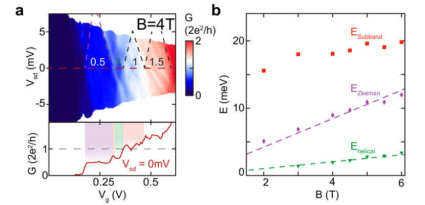
Voltage bias spectroscopy, as shown in Fig 3a confirms that this state evolves as a constant energy feature. By analyzing the voltage bias spectroscopy data at a range of magnetic fields, we quantify the development of the initial plateau, as well as the reentrant conductance feature (Fig 3b). From the evolution of the width of the first plateau, we can calculate the -factor of the first sub-band . This number is consistent with the recent experiments, which reported g factors of .van2012quantized ; nadj2012spectroscopy Comparing the slopes of the Zeeman gap and the helical gap provides an alternative way to determine the offset angle . We find which is in reasonable agreement with the angle determined by magnetic field rotation.
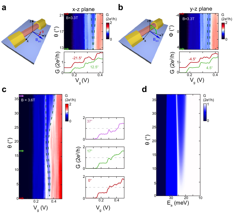
To confirm that the reentrant conductance feature agrees with spin orbit theory, we rotate the magnetic field in the plane of the substrate at a constant magnitude , as shown in Fig 4a. When the field is rotated towards being parallel to , the conductance dip closes, while when it is rotated away from , the dip increases in width and depth. In contrast, when the magnetic field is rotated the same amount around the y-z plane, which is largely perpendicular to , there is little change in the reentrant conductance feature, as shown in Fig 4b. Figure 4c shows the result of rotating through a larger angle in the x-y plane shows this feature clearly evolves with what is expected for spin orbit. Our numerical simulations in Figure 4d agree well with the observed experimental data. The small difference in the angle evolution between the numerical simulations and experimental data can be attributed to imperfect alignment of the substrate with the x-y plane.
The extracted SO energy of is significantly larger than that obtained via other techniques, such as weak anti localization (WAL) measurements,van2015spin and quantum dot spectroscopy.nadj2012spectroscopy This is not entirely unexpected, due to the differing geometry for this device and different conductance regime it is operated in. Quantum dot measurements require strong confinement, and so the Rashba SOI is modified by the local electrostatic gates used to define the quantum dot. Weak anti-localization measurements are performed in an open conductance regime, however they assume transport through a diffusive, rather than a ballistic channel. Neither of these measurements explicitly probe the spin orbit interaction where exactly one mode is transmitting in the nanowire, the ideal regime for Majoranas, and so the spin orbit parameters extracted from QPC measurements offer a more accurate measurement of the SOI experienced by the Majorana zero mode. Also, the SOI in a nanowire can be different for every subband, and it is expected that the lowest mode has the strongest spin-orbit due to a smaller confinement energy.winkler2003 Additionally, the finite diameter of the nanowire, together with impurities within the InSb crystal lattice both break the internal symmetry of the crystal lattice and may contribute a non-zero Dresselhaus component to the spin orbit energy that has not been previously considered. While high quality quantized conductance measurements have been previously achieved in short channel deviceskammhuber2016conductance (), the channel lengths required for observing the helical gap are at the experimental limit of observable conductance quantization. As shown in the Supplementary Information, small changes in the QPC channel length, spin-orbit strength or the QPC potential profile are enough to obscure the helical gap, particularly for wires with weaker SOI. We have fabricated and measured a range of QPCs with different length and potential profiles, and only two devices of showed unambiguous signatures of a helical gap.
Several phenomena have been reported to result in anomalous conductance features in a device such as this. Oscillations in conductance due to Fabry-Perot resonances are a common feature in clean QPCs. Typically the first oscillation at the front of each plateau is the strongest and the oscillations monotonically decrease in strength further along each plateau.Rainis2014 ; van2015spin In our second device, we clearly observe Fabry-Perot conductance oscillations at the beginning of each plateau, however these oscillations are significantly weaker than the subsequent conductance dip. Furthermore we observe Fabry-Perot oscillations at each conductance plateau, while the reentrant conductance feature is only present at the plateau. Additionally, the width of the Fabry-Perot oscillations does not change with increasing magnetic field, unlike the observed re-entrant conductance feature. A local quantum dot in the Coulomb or Kondo regimes can lead to conductance suppression, which increases in magnetic field.heyder2015relation However both effects should be stronger in the lower conductance region, and exists at zero magnetic field, unlike the feature in our data. Additionally, a Kondo resonance should scale with as a function of external magnetic field, decreasing instead of increasing the width of the region of suppressed conductance. Given the g factor measured in InSb quantum dots, and its variation with the angle of applied magnetic field ,nadj2012spectroscopy we can exclude both these effects. Similarly the Fano effect and disorder can also induce a conductance dip, but these effects should not increase linearly with magnetic field. The 0.7 anomaly occurs at the beginning of the plateau, and numerical studies have shown it does not drastically affect the observation of the helical gap.Goulko2014 In conclusion, we have observed a return to conductance at the plateau in a QPC in an InSb nanowire. The continuous evolution in increasing magnetic field and the strong angle dependence in magnetic field rotations agree with a SOI related origin of this feature and distinguish it from Fabry-Perot oscillations and other g-factor related phenomena. Additional confirmation is given by numerical simulations of an emerging helical gap in InSb nanowires. The extracted spin orbit energy of is significantly larger than what has been found by other techniques, and more accurately represents the true spin orbit energy in the first conduction mode. Such a large spin orbit energy reduces the requirements on nanowire disorder for reaching the topological regime,sau2012experimental and offers promise for using InSb nanowires for the creation of topologically protected quantum computing devices.
Methods
Device Fabrication
The InSb nanowires were grown using the metalorganic vapor phase epitaxy (MOVPE) process.28 The InSb nanowires were deposited using a deterministic deposition method on a degenerately doped silicon wafer. The wafer covered with of low stress LPCVD SiN which is used as a high quality dielectric. Electrical contacts (Cr/Au, /) defined using ebeam lithography were then evaporated at the ends of the wire. Before evaporation the wire was exposed to an ammonium polysulfide surface treatment and short helium ion etch to remove the surface oxide and to dope the nanowire underneath the contacts.kammhuber2016conductance
Measurements
Measurements are performed in a dilution refrigerator with base temperature fitted with a 3-axis vector magnet, which allowed for the external magnetic field to be rotated in-situ. The sample is mounted with the substrate in the x-y plane with the wire orientated at a small offset angle from the x-axis. We measure the differential conductance using standard lock-in techniques with an excitation voltage of and frequency . Additional resistances due to filtering are subtracted to give the true conductance through the device.
Numerical transport simulations
We use the method of finite differences to discretize the one-dimensional nanowire model of Ref 2. In order to obtain a one-dimensional QPC potential, we solve the Poisson equation self-consistently for the full three-dimensional device structure treating the charge density in the nanowire in Thomas-Fermi approximation. To this end, we use a finite element method, using the software FEniCS.logg2012automated The resulting three-dimensional potential is then projected onto the lowest nanowire subband and interpolated using the QPC potential model of Ref Rainis2014 . Transport in the resulting tight-binding model is calculated using the software Kwant.groth2014kwant
References
- (1) Středa, P. & Šeba, P. Antisymmetric Spin Filtering in One-Dimensional Electron Systems with Uniform Spin-Orbit Coupling. Phys. Rev. Lett. 90, 256601 (2003)
- (2) Pershin, Y. V., Nesteroff, J. A. & Privman, Vladimir Effect of spin-orbit interaction and in-plane magnetic field on the conductance of a quasi-one-dimensional system. Phys. Rev. B 69, 212306 (2004)
- (3) Sato, K., Loss, D. & Tserkovnyak, Y. Cooper-Pair Injection into Quantum Spin Hall Insulators. Phys. Rev. Lett. 105, 1-4 (2010)
- (4) Shekhter, R. I., Entin-Wohlman, O., Jonson, M. & Aharony, A. Rashba Splitting of Cooper Pairs. Phys. Rev. Lett. 116, 1-6 (2016)
- (5) Alicea, J., Oreg, Y., Refael, G., Von Oppen, F. & Fisher, M. P. A. Non-Abelian statistics and topological quantum information processing in 1D wire networks. Nat. Phys. 7, 412-417 (2011)
- (6) Nayak, C., Simon, S. H., Stern, A., Freedman, M. & Das Sarma, S. Non-Abelian anyons and topological quantum computation. Rev. Mod. Phys. 80, 1083–1159 (2008)
- (7) Oreg, Y., Refael, G. & von Oppen, F, Helical Liquids and Majorana Bound States in Quantum Wires. Phys. Rev. Lett. 105, 1-4 (2010)
- (8) Dresselhaus, G. Spin-Orbit Coupling Effects in Zinc Blende Structures. Phys. Rev. 100, 580-586 (1955)
- (9) Rashba, E. & Sheka, V. Symmetry of Energy Bands in Crystals of Wurtzite Type II. Symmetry of Bands with Spin-Orbit Interaction Included. Fiz. Tverd. Tela Collect. Pap. 2, 162–176 (1959)
- (10) Winkler, R. Spin-orbit Coupling Effects in Two-Dimensional Electron and Hole Systems. (Springer-Verlag Berlin Heidelberg, 2003) , ()
- (11) König, M. et al. Quantum Spin Hall Insulator State in HgTe Quantum Wells. Science (80-. ). 318, 766–771 (2007)
- (12) Nowack, K. C. et al. Imaging currents in HgTe quantum wells in the quantum spin Hall regime. Nat. Mater. 12, 787–791 (2013)
- (13) Quay, C. H. L., Hughes, T. L., Sulpizio, J. A., Pfeiffer, L.N. , Baldwin, K. W., West, K.W., Goldhaber-Gordon, D. & De Picciotto, R. Observation of a one-dimensional spin–orbit gap in a quantum wire. Nat. Phys. 6, 336–339 (2010).
- (14) Klinovaja, J., Schmidt, M. J., Braunecker, B. & Loss, D. Helical modes in carbon nanotubes generated by strong electric fields. Phys. Rev. Lett. 106, 1–4 (2011).
- (15) Klinovaja, J., Stano, P., Yazdani, A. & Loss, D. Topological superconductivity and Majorana fermions in RKKY systems. Phys. Rev. Lett. 111, 1–5 (2013).
- (16) Mourik, V., Zuo, K.,Frolov, S. M., Plissard, S.R., Bakkers, E. P. A. M. & Kouwenhoven, L. P. Signatures of Majorana Fermions in hybrid superconductor-semiconductor nanowire devices. Science (80-. ). 336, 1003 (2012).
- (17) Albrecht, S. M. et al. Exponential Protection of Zero Modes in Majorana Islands. Nature 531, 206–209 (2016).
- (18) Rainis, D. & Loss, D. Conductance behavior in nanowires with spin-orbit interaction: A numerical study. Phys. Rev. B 90, 1–9 (2014).
- (19) Kammhuber, J. et al. Conductance Quantization at Zero Magnetic Field in InSb Nanowires. Nano Lett. 16, 3482–3486 (2016).
- (20) Heedt, S., Prost, W., Schubert, J., Grützmacher, D. & Schäpers, T. Ballistic Transport and Exchange Interaction in InAs Nanowire Quantum Point Contacts. Nano Lett. 16, 3116–3123 (2016).
- (21) Van Weperen, I., Plissard, S. R., Bakkers, E. P. A. M., Frolov, S. M., Kouwenhoven, L. P. Quantized conductance in an InSb nanowire. Nano Lett. 13, 387–391 (2013).
- (22) Nadj-Perge, S. et al. Spectroscopy of spin-orbit quantum bits in indium antimonide nanowires. Phys. Rev. Lett. 108, 1–5 (2012).
- (23) Van Weperen, I. et al. Spin-orbit interaction in InSb nanowires. Phys. Rev. B 91, 1–17 (2015).
- (24) Cayao, J., Prada, E. , San-Jose, P. & Aguado, R. SNS junctions in nanowires with spin-orbit coupling: Role of confinement and helicity on the subgap spectrum. Phys. Rev. B 91, 24514 (2015).
- (25) Heyder, J. et al. Relation between the 0.7 anomaly and the Kondo effect: Geometric crossover between a quantum point contact and a Kondo quantum dot. Phys. Rev. B 92, (2015).
- (26) Goulko, O., Bauer, F., Heyder, J. & Von Delft, J. Effect of spin-orbit interactions on the 0.7 anomaly in quantum point contacts. Phys. Rev. Lett. 113, 1–5 (2014).
- (27) Sau, J. D., Tewari, S. & Das Sarma, S. Experimental and materials considerations for the topological superconducting state in electron- and hole-doped semiconductors: Searching for non-Abelian Majorana modes in 1D nanowires and 2D heterostructures. Phys. Rev. B 85, 1–11 (2012).
- (28) Plissard, S. R. et al. From InSb nanowires to nanocubes: Looking for the sweet spot. Nano Lett. 12, 1794–1798 (2012).
- (29) Logg, A., Mardal, K.-A., Wells, G. N. et al. Automated Solution of Differential Equations by the Finite Element Method, Springer, 2012.
- (30) C. W. Groth, C. W., Wimmer, M., Akhmerov, A. R., Waintal, X., Kwant: a software package for quantum transport, New J. Phys. 16, 063065 (2014)
Acknowledgements.
We gratefully acknowledge D. Xu, Ö. Gül, S. Goswami, D. van Woerkom and R.N. Schouten for their technical assistance and helpful discussions. This work has been supported by funding from the Netherlands Foundation for Fundamental Research on Matter (FOM), the Netherlands Organization for Scientific Research (NWO/OCW), the Office of Naval Research, Microsoft Corporation Station Q, the European Research Council (ERC) and an EU Marie-Curie ITN.Author contributions
J.K and F.P. fabricated the samples, J.K. M.C.C. and F.P. performed the measurements with input from M.W.. M.W., M.N. and A.V. developed the theoretical model and performed simulations. D.C., S.R.P. and E.P.A.M.B. grew the InSb nanowires. All authors discussed the data and contributed to the manuscript.
Supplementary Information for: Conductance through a helical state in an InSb nanowire
J. Kammhuber,1 M. C. Cassidy,1 F. Pei,1 M. P. Nowak,1,2 A. Vuik,1 D. Car,1,3
S. R. Plissard,4 E. P. A. M. Bakkers,1,3 M. Wimmer,1 Leo P. Kouwenhoven1,∗
1QuTech and Kavli Institute of Nanoscience, Delft University of Technology, 2600 GA Delft, The Netherlands
2 Current adress: Faculty of Physics and Applied Computer Science, AGH University of Science and Technology, al. A.Mickiewicza 30, 30-059 Kraków, Poland
3Department of Applied Physics, Eindhoven University of Technology, 5600 MB Eindhoven, The Netherlands
4CNRS-Laboratoire d’Analyse et d’Architecture des Systemes (LAAS), Université de Toulouse, 7 avenue du colonel Roche, F-31400 Toulouse, France
I Numerical simulations of the conductance through a helical states
I.1 Poisson calculations in a 3D nanowire device
Observing the helical gap in a semiconducting nanowire crucially depends on the smoothness of the electrostatic potential profile between the two contacts supp1 . When the potential profile changes too abruptly, it forms a tunnel barrier which suppresses conductance well below quantized values, thereby masking features of the helical gap. On the other hand, if the potential varies on a length scale much larger than the characteristic spin-orbit coupling length , transmission through the ‘internal state’ (the smaller-momentum state of the two right-moving states in the bottom of the lower band) is suppressed. This reduces the first plateau in the conductance to a plateau, thereby concealing again the helical gap.
Because of the crucial role of the electrostatic potential, we perform realistic Poisson calculations to compute the potential in the nanowire (with ), solving the Poisson equation of the general form
| (S1) |
with the dielectric permittivity and the charge density. For the charge density , we apply the Thomas-Fermi approximation supp2
| (S2) |
where is the effective mass of InSb.
For a given charge density , we solve Eq. S1 numerically for the potential using the finite element package FEniCS supp3 . We model the two normal contacts as metals with a fixed potential V, assuming a small work function difference between the nanowire and the normal contacts. The back gate is modeled as a fixed potential along the bottom surface of the dielectric layer. We use the dielectric permittivities for InSb and SiN in the wire and the dielectric layer respectively. The FEM mesh, with its dimensions and boundary conditions, is depicted in Fig. S1a.
We apply the Anderson mixing scheme supp4 to solve the nonlinear equation formed by Eqs. S1 and S2 self-consistently. An example of a self-consistent Poisson potential with Thomas-Fermi density is plotted in Fig. S1b.
I.2 Conductance calculations in a 1D model with a projected potential barrier
To apply the 3D Poisson potential in a simple 1D nanowire model, we convert the three-dimensional potential to a one-dimensional effective potential barrier by projecting on the transverse wave functions in the nanowire:
| (S3) |
To do this, we compute the eigenenergies of the Hamiltonian of a two-dimensional cross section at a point along the wire, with a corresponding potential . The effective potential barrier is then given by the ground state of the Hamiltonian. The longitudinal variation of the potential barrier is obtained by computing the ground state of the transverse Hamiltonian at many points along the wire. An example of the projected potential is given in Fig. S1c with the solid-black curve.
Due to rough boundary conditions in the FEM mesh (see the edges of the dielectric layer and the normal contacts in the potential of Fig. S1b), the projected potential shows some roughness that may cause unwanted scattering events (see black curve in Fig. S1c). To avoid this, we fit to a linear combination of hyperbolic tangents, given by
| (S4) |
Here, is the amplitude, the width and the downshift in energy of the potential barrier, which varies along on a typical length scale , as indicated in Fig. S1c. The horizontal shift of the barrier to the middle of the nanowire is denoted by nm.
The parameter expresses the smoothness of the barrier. We find that is close to zero when no charge is present in the wire and the boundary conditions result in an abrupt step in the potential between the contacts and the uncovered part of the wire. When charge enters the wire, it screens the electric field, thereby smoothening the potential. For a QPC length of 325 nm we find in this regime nm. The value of is reduced for smaller QPC lengths, but saturates to nm for longer QPC lengths. Moreover we find that has only a little dependency on the back gate voltage or the applied magnetic field (Fig. S1d). Taking advantage of the latter and the fact that we are interested in the conductance of the wire in the vicinity of the helical-gap feature – where the screening is present – we assume constant in space for the conductance calculation.
For the conductance calculations we consider transport through a two-mode nanowire described by the Hamiltonian
| (S5) |
where denote the Pauli matrices (with the identity matrix) and is fit to the projected potential barrier, as expressed in Eqs. S3 and S4. Spin-orbit coupling strength is given by where we use as a free parameter. We take the effective mass of InSb and (unless stated otherwise) as estimated in the main text. Note that for the coordinate system used here, where the wire lies along the x direction and is the angle between and the external magnetic field. The Hamiltonian Eq. S5 is discretized on a mesh with lattice spacing nm. Assuming translational invariance of the boundary conditions at the ends of the wire one arrives at the scattering problem that is solved using the Kwant package supp5 to obtain the linear-response conductance within the Landauer-Büttiker formalism.
II Angle-dependence of conductance in Rashba nanowires
II.1 Theoretical model
We consider a one-dimensional nanowire with Rashba spin-orbit interaction (SOI) in an external magnetic field . The field is oriented at an angle with respect to the effective magnetic field due to Rashba SOI, as shown in Fig. S1e. This setup is described by the Hamiltonian:supp6
| (S6) |
In this expression, is the momentum operator, is the effective mass, the Rashba SOI-strength, and the Pauli matrices. The Zeeman energy , where is the g-factor, and the Bohr magneton. In Eq. (S6) we assumed without loss of generality a magnetic field in the x-y-plane; the band structure however only depends on the relative angle of with .
The Rashba SO-strength can be related to an effective length scale, the spin-orbit length
| (S7) |
and to an energy scale, the spin-orbit energy
| (S8) |
Defining length in units of and energy in units of it is possible to write the Hamiltonian in a convenient dimensionless form:
| (S9) |
Proper units will be restored in the final result.
In an translationally invariant nanowire, the wave vector is a good quantum number and the Rashba Hamiltonian is readily diagonalized as supp6
| (S10) |
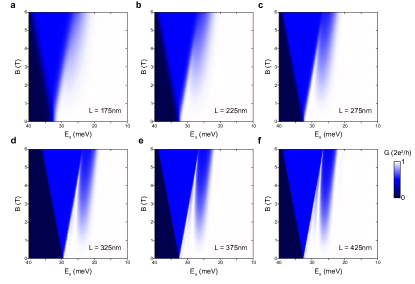
The resulting band structure for a general angle is shown schematically in the left panel of Fig. S1f. The band structure can be related to an idealized quantum point contact (QPC) conductance by counting the number of propagating modes at a given energy (see right panel of Fig. S1f).
In the following we will derive from the band structure: (i) the size of the plateaus in energy (denoted by and ). This is directly measurable using the finite bias dependence of the QPC conductance (measuring so-called QPC diamonds). (ii) The critical field for which the spin-orbit induced conductance (the size of this plateau is denoted as ) vanishes. This allows for an estimate of the spin-orbit strength from the magnetic field dependence in experiment.
II.2 Size of Zeeman-induced gaps
In order to compute the size of the different QPC plateaus in energies, we need to compute the value of the minima and maxima of the bands . This can be done exactly using a computer algebra program (we used Mathematica), as it only involves solving for the roots of polynomials up to fourth order. The resulting expressions are however quite cumbersome, and it is more useful to find an approximate expression doing a Taylor approximation. Up to second order in we then find the simple expressions
| (S11) | ||||
| (S12) |
II.3 Critical magnetic field for the spin-orbit induced -plateau
The spin-orbit induced region persists only up to a critical Zeeman splitting , after which the two -plateaus merge into one. In the band structure, this corresponds to a transition from three extrema in (two minima, one maximum) to only one minimum. The critical Zeeman splitting where this happens can be solved for exactly using Mathematica:
| (S13) |
where
| (S14) | ||||
| (S15) |
For this gives and for . When the value of the nanowire g-factor is extracted from experiment, the critical Zeeman splitting can be translated into a critical magnetic field. The magnetic field up to which the spin-orbit induced -plateau is still visible in experiment can then be used to set a lower bound on the spin-orbit energy. It is a lower bound, as for a given QPC potential the may not be visible any more despite in principle being present in the band structure. A more detailed transport calculation can be used to improve on this bound.
III Device 1 - Additional Data
IV Device 2 - Data
V Control devices
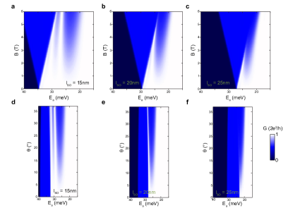
V.1 QPC length dependence
V.2 Simulations - length dependence
VI Simulations - Angle dependence
VII Simulations - Spin Orbit Strenght
References
- (1) D. Rainis and D. Loss Conductance behavior in nanowires with spin-orbit interaction: A numerical study. Phys. Rev. B 90, 235415 (2014).
- (2) N. March The Thomas-Fermi approximation in quantum mechanics. Advances in Physics 6, 1 (1957)
- (3) A. Logg, K.-A. Mardal, G. N. Wells, et al., Automated Solution of Differential Equations by the Finite Element Method (Springer, 2012).
- (4) V. Eyert, Journal of Computational Physics 124, 271 (1996).
- (5) C. W. Groth, M. Wimmer, A. R. Akhmerov, and X. Waintal, New Journal of Physics 16, 063065 (2014)
- (6) Y. V. Pershin, J. A. Nesteroff, and V. Privman, Phys. Rev. B 69, 121306 (2004)