From Half-metal to Semiconductor: Electron-correlation Effects in Zigzag SiC Nanoribbons From First Principles
Abstract
We performed electronic structure calculations based on the first-principles many-body theory approach in order to study quasiparticle band gaps, and optical absorption spectra of hydrogen-passivated zigzag SiC nanoribbons. Self-energy corrections are included using the GW approximation, and excitonic effects are included using the Bethe-Salpeter equation. We have systematically studied nanoribbons that have widths between 0.6 nm and 2.2 nm. Quasiparticle corrections widened the Kohn-Sham band gaps because of enhanced interaction effects, caused by reduced dimensionality. Zigzag SiC nanoribbons with widths larger than 1 nm, exhibit half-metallicity at the mean-field level. The self-energy corrections increased band gaps substantially, thereby transforming the half-metallic zigzag SiC nanoribbons, to narrow gap spin-polarized semiconductors. Optical absorption spectra of these nanoribbons get dramatically modified upon inclusion of electron-hole interactions, and the narrowest ribbon exhibits strongly bound excitons, with binding energy of 2.1 eV. Thus, the narrowest zigzag SiC nanoribbon has the potential to be used in optoelectronic devices operating in the IR region of the spectrum, while the broader ones, exhibiting spin polarization, can be utilized in spintronic applications.
I Introduction
After the synthesis of graphene 1, and the discovery of its unique electronic, optical and thermal properties, research on low-dimensional materials has increased tremendously. Graphene is attractive because of its unique properties such as its high electronic conductivity, and high mobility at room temperature 2; 3; 4. However its applications are limited in semiconducting devices because of its zero band gap. This gaplessness of graphene has motivated the discovery of alternate nanomaterials that possess finite band gap, and have the potential to replace the silicon in semiconductor technology. Recently two-dimensional (2D) materials which have finite band gap such as monolayers of hexagonal boron-nitride (h-BN) 5, transition metal chalcogenides (MoS2, WS2 etc.)6; 7, and phosphorene have been successfully synthesized8.
Quasi one-dimensional materials such as nanoribbons, nanotubes, nanorods, and nanowires have also attracted attention because of their interesting photochemical, photophysical, and transport properties9; 10. Nanoribbons (NRs), in particular, have received great attention from researchers because of their unique electronic properties which can be modified on the basis of their edge configuration, and width. Quantum confinement because of the presence of edges, and their different possible passivations, lead to interesting optical, electronic and magnetic properties. Graphene nanoribbons (GNRs) and boron-nitride nanoribbons (BNNRs) have been experimentally synthesized by unwrapping of carbon nanotubes, and BN nanotubes, respectively11; 12. Armchair GNRs (AGNRs) are non magnetic semiconductors for all widths, and have oscillating band gaps over families, approaching the zero band gap of a 2D sheet, for large widths13. Zigzag GNRs (ZGNRs), on the other hand, have tunable band gaps ranging from metal to semiconductor, depending on the width, and passivation edges14; 15. Furthermore, ZGNRs also exhibit half-metallic behavior with spin-polarized band gaps when an electric field is applied along the direction of the width of the ribbons, and their gaps can be controlled by the strength of the electric field16.
C and Si have same number of electrons, therefore SiC structures are stable in bulk and have electronic properties which are intermediate in between bulk Si and carbon structures. Silicon carbide (SiC) crystallizes in several forms such as hexagonal, rhombohedral, and cubic Bravais lattices17. Bulk SiC is a wide band gap semiconductor, and has been used in high-temperature, high-pressure and high-frequency device applications18; 19. The graphene-like 2D SiC monolayer has not been experimentally fabricated yet, but has been extensively studied using theoretical methods20; 21; 22; 23; 24; 25; 26; 27; 28; 29. Unlike graphene, it is a direct band gap semiconductor with a band gap of 2.5 eV. An ultra-thin SiC nanosheet which has a thickness of has been fabricated, and is used in light emitting applications 30. Various SiC structures such as SiC nanotubes, SiC nanowires, microribbons, and crystalline and bicrystalline nanobelts have also been successfully synthesized31; 32; 33; 34. Furthermore multilayer SiC nanoribbons in lengths of micrometers, and thicknesses of nanometers have also been synthesized35.
As far as theory is concerned, SiC nanoribbons have been extensively studied using first-principles calculations, based on the density functional theory approach (DFT) 21; 36; 37; 38; 17; 22; 39; 40; 41; 42; 43. Sun et al. 21 reported that hydrogen- passivated armchair SiCNRs (ASiCNRs) are direct band gap semiconductors, with band gaps in the range of 2.3 - 2.4 eV. Furthermore, they reported that band gaps of zigzag SiCNRs (ZSiCNRs) are spin polarized, and exhibit intrinsic half-metallic behavior, without the application of an external electric field.21 Lou et al.36 studied narrow ZSiCNRs with widths in the range 0.6–1.6 nm, and showed that the ferrimagnetic state is more stable, with an anti parallel spin orientation between the two edges. ZSiCNRs that have a half-bare-edge were studied by Tang et al.42 using hybrid DFT approach. They reported that half-bare-edge ZSiCNRs with a bare carbon edge are magnetic semiconductors, while the ones with bare Si edge atoms are magnetic metals. The influence of doping with B and N impurities has been studied by Costa et al.,41 who showed that B doped ZSiCNRs retain half metallic behaviour, while N doped ZSiCNRs become metallic. Lopez-Benzanilla et al.39 employed a local spin-density approximation (LSDA) approach to study sulfur and oxygen passivated ZSiCNRs to discover that, ZSiCNRs turned from half-metallic to semiconductors, or metals, as a result of passivation. The effects of substitution of edge atoms, with B and N atoms, has been studied by Zheng et al.40 who reported that modified ZSiCNRs are semiconductors. Bekaroglu et al.,22 and Morbec et al.,43 studied the effects of vacancies on the electronic structure of ZSiCNRs by using the DFT-GGA approach, and found that double (Si and C) vacancies induce magnetism. Ultra narrow ZSiCNRs were studied by Ping et al.44 including short-range exact exchange effects, and they obtained lower edge energies, and higher band gaps, as compared to the ones computed using GGA.
It is well known that the DFT-based approaches underestimate the band gap in semiconductors, because they do not include electron correlation effects.45 It has been demonstrated that in nanoribbons, not including correlation effects causes severe errors as compared to their bulk counterpart, because in low-dimensional systems these effects are enhanced 46; 47; 48; 49; 50; 51; 52. It will be also be interesting to study many-body electron-electron interactions in evaluating accurate band gaps and electron-hole effects in order to calculate optical absorption spectra in ZSiCNRs; this knowledge will enable the exploration of their potential in optical device applications. In the present work, we calculate the quasiparticle band structures and the optical absorption spectra of ZSiCNRs by using GW approximation, and by solving the Bethe-Salpeter equation (BSE), respectively. We find that ultra-narrow ZSiCNRs, with widths narrower than 1 nm, are non-magnetic semiconductors. GW corrections open up significant band gaps in ZSiCNRs that are wider than 1 nm, and transform them from half-metals to semiconductors. We find that narrowest ZSiCNR, with the width of 0.6 nm, has strongly bound excitons, with a binding energy of 2.1 eV, while other nanoribbons have weakly bound excitons because their band gaps are too small. Therefore, the narrowest ribbon can be utilized in optoelectronic applications in the infrared frequency range. Broader nanoribbons exhibit distinct band gaps for the two spin orientations, and, therefore, they can be utilized in spintronic devices such as spin valves.
II Computational Details
We carried out first-principles many-body electronic structure calculations for ZSiCNRs using a three-step procedure. Firstly, the DFT calculations are performed using a plane wave approach, in the generalized gradient approximation (GGA),53 with Perdew-Burke-Enzerhof (PBE) pseudopotentials.54 Geometry optimizations were carried out using the computer program Vienna ab initio simulation package (VASP) 55. All the nanoribbons considered here were fully relaxed until the force on each atom was lower than 0.01 eV/Å. The threshold energy convergence was set to eV. A Monokhorst k-point grid of was used for Brillouin zone integration during the relaxation. After the relaxation, we used optimized atomic positions and lattice parameters to calculate Kohn-Sham band gaps of ZSiCNRs using the DFT-GGA approach as implemented in the software package ABINIT 56; 57. GGA wave functions are a good starting point for the many-body calculations, aimed at including electron correlation effetcs.
In the second step we calculate quasiparticle corrections for the DFT-GGA band gaps using the many-body approach G0W0 approximation58, which is a single-shot GW approach for computing self-energy corrections in terms of the Green’s function (G), and the screened Coulomb potential (W). The screening effects were included by using the plasmon pole model59. A kinetic energy cutoff of 26 Ha has been used for all the systems considered here. Cutoff energies of 5 Ha, and 12 Ha have been used for the correlation, and the exchange, parts of self-energy calculations, respectively. A total number of 200 bands were used, out of which more than 120 were unoccupied. In the last step, the BSE is solved within the Tamm-Dancoff approximation60 in order to obtain the optical response inclusive of the contribution of the electron-hole interactions, retaining only the resonant part of the Bethe-Salpeter Hamiltonian: This is because the inclusion of the coupling has been shown to have a negligible effect. This approximation has been also used to study similar systems such as graphene nanoribbons,46; 61 and boron-nitride nanoribbons49. In the GW, and the BSE calculations, a Coulomb truncation scheme was also used to avoid the inclusion of long range interactions between the periodic images. A k-point grid has been used in the the GW and BSE calculations for the systems considered here. Five valence band and five conduction bands were included to obtain the optical absorption spectra. Nanoribbons were considered to be periodic along the direction, and more than 13 Å wide vacuum layers were taken in non-periodic directions ( and directions), in order to represent an isolated system. Width of a given ZSiCNR was specified by prefixing it with the number of zigzag lines () across its width. Thus ZSiCNR-3 denotes a ribbon with =3 zigzag lines across the width. In the present work, we have studied ribbons with , which corresponds to widths between 0.6 nm and 2.2 nm.
III Results And Discussion
III.1 Formation energy and stability
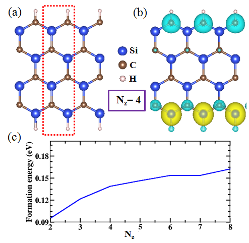
Fig. 1 (a) shows the geometric structure of ZSiCNR-4. Optimized bond lengths corresponding to Si-C, Si-H, and C-H were obtained to be 1.77 Å, 1.49 Å, and 1.09 Å, respectively, while the lattice constant was found to be 3.11 Å, for all the structures considered here. These parameters are in good agreement with previous studies21; 44. Here, we calculate the edge formation energies of these nanoribbons in order to understand their thermodynamic stability, during edge formation. We evaluated the formation energy by using the following formula:
where is the total energy of the hydrogen passivated zigzag SiC nanoribbon , is the total energy of the 2D SiC sheet, is the total energy of an isolated hydrogen molecule, is the number of SiC dimers in the unit cell, is the number of H atoms in the unit cell, and is the periodic length of an edge. In general, the lower the value of of a material, the higher its stability. The formation energy of ZSiCNRs as a function of width has been plotted in Fig. 1 (c). Unlike ASiCNRs,52 formation energy of these nanoribbons is strongly dependent on their width, and it increases with the width of the nanoribbons. From the figure it is obvious that ribbons which have narrow widths have high stability, suggesting that they will be relatively easier to synthesize in the laboratory.
III.2 Nonmagnetic ZSiCNRs
III.2.1 Quasiparticle energies
First we discuss the electronic structure of ZSiCNRs with widths and 3, which do not exhibit any magnetic behavior. Ping et al. 44 reported that these two nanoribbons are non-magnetic semiconductors, which do not exhibit half-metallic behaviour within the GGA or HSE approaches, unlike ribbons which are wider than 1 nm. Their DFT-GGA study predicted that ZSiCNR-2 is a non-magnetic semiconductor with a band gap of 0.97 eV, and ZSiCNR-3 is essentially metallic with a band gap of 0.07 eV. Our calculated DFT-GGA and GW band structures of ZSiCNR-2 and ZSiCNR-3 are shown in Figs. 2 (a) and (b ) respectively. The blue lines correspond to the DFT-GGA, while the red lines denote the GW band structure. Our DFT results agree with those of Ping et al 44. Fig. 2 (a) shows that ZSiCNR-2 is a direct band gap material at the DFT-GGA level, and the gap occurs at the point located at the edge of Brillioun zone. After including the many-body effects, computed band structure is depicted by the red lines. We found that quasiparticle corrections increase the band gap from 0.97 to 2.4 eV, which is an indirect one (quasi-direct) at the GW level. In the GW band structure of ZSiCNR-2, the valence band maximum (VBM) occurs small distance away from the point, and there is no change in the conduction band minimum (CBM). Fig. 2 (b) shows the band structures computed by GGA and GW approaches, for ZSiCNR-3. Self-energy corrections widened the band gap from 0.07 eV to 0.45 eV, which is a six fold increase due to electron correlation effects. This increase shows that many-body corrections transform ZSiCNR-3 from a nearly metallic system, to a semiconductor.
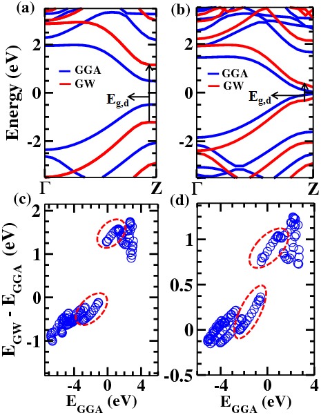
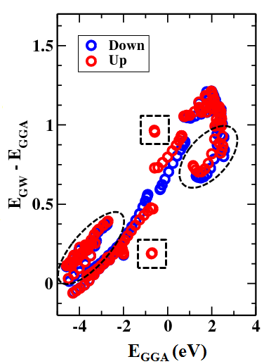
Self-energy corrections for various bands for both the ribbons are shown in Figs. 2 (c) and (d). In these nanoribbons, band states corresponding to the orbital extend into the vacuum perpendicular to the ribbon plane, while the states are composed of and orbitals lying in the plane of the sheet. The self-energy corrections to the states are larger than those to the states because of the screening effects due to other electrons . The corrections enclosed in the red ellipses correspond to the edge states which experience enhanced Coulombic interactions. When compared to GGA band structure, GW bands not only shift but also stretch by an average of 20%-30% because of non-uniform quasiparticle corrections. We find that corrections to the states which derive main contribution from the interior atoms are less linear when compared to states which are predominantly localized on edge atoms.
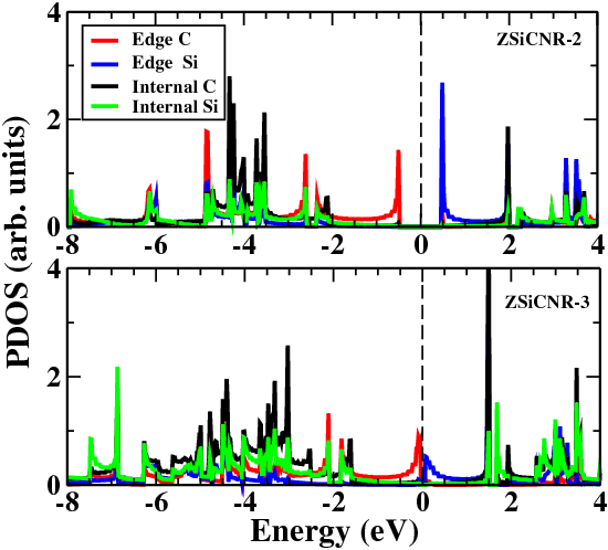
We present projected density of states (PDOS) for ZSiCNR-2 and ZSiCNR-3 in Fig. 3, in order to illustrate the contribution of various atoms from the edges, and the interior, to different orbitals. PDOS plots show that the VBM in both the ribbons arises from edge carbon atoms, while the CBM is derived from edge Si atoms. The states located on internal C and Si atoms are away from the Fermi-level in both the ribbons.
III.2.2 Optical absorption spectra
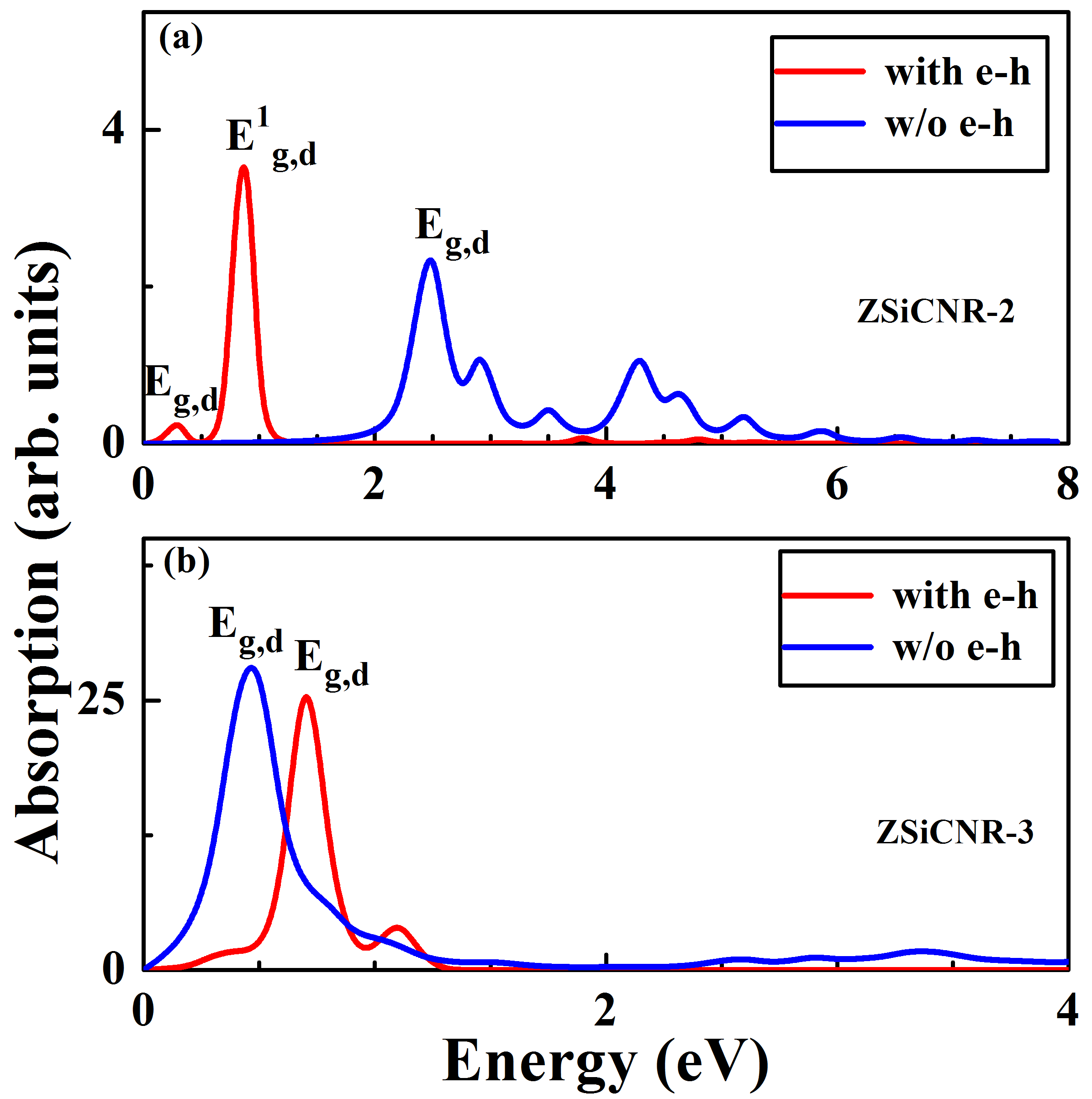
Using the quasiparticle band structure, we calculated the optical absorption spectrum of the ZSiCNR-2 and ZSiCNR-3, with, and without electron-hole interactions as is shown in Figs. 4 (a) and (b). Electron-hole interactions were incorporated by using the BSE, and in all the calculations the polarization direction of incident light was considered to be along the length of the nanoribbons. We use notation to label the direct transitions which occur between first valence band and first conduction band as shown in Fig. 2. The blue curve represents absorption due to interband transitions at the GW-RPA level, while the red curve is a result of solving the BSE, including electron-hole effects. In both the ribbons, the first prominent peak comes from the transition between the first valence band, and the first conduction band. In GW-RPA absorption spectra we can observe that there are several peaks due to different interband transitions in ZSiCNR-2. However, there is only one prominent peak in ZSiCNR-3 which is a result of the transition between the VBM and the CBM. The inclusion of electron-hole interactions changes the spectrum significantly because, not only the positions of the peaks are shifted, but also their shape looks different, when compared with the GW-RPA absorption spectrum. In the absorption spectra of both the ribbons, which include electron-hole interactions, we observe only one intense excitonic peak due to the transition between first valence and first conduction band, . We did not find any other transitions among other bands, even though we included five valence and five conduction bands in our calculations. In Fig. 4 it is obvious that ZSiCNR-2 has a strongly bound exciton, of binding energy of 2.1 eV (), but with relatively weaker intensity, corresponding to the first absorption peak. We also observed another strongly bound excitonic peak (), with a very high intensity, and binding energy of 1.5 eV, originating at distinct -points as compared to the first one. These binding energies are significantly larger than the calculated exciton binding energy, 1.17 eV, for the 2D SiC sheet,25 suggesting that the reduced dimensionality, and quantum confinement, lead to an enhancement in the exciton binding energies of nanoribbons. From among all the ribbons considered here, it is clear that ZSiCNR-2 is a small gap semiconductor which can be used in optical applications in the low energy region of spectrum. Unlike ZSiCNR-2, strongly bound excitons are not observed in ZSiCNR-3 because the band gap is much smaller for this ribbon. Band to band absorption spectrum peak at GW level gets blue shifted upon inclusion of electron-hole effects, as shown in Fig. 4. The final location of the blueshifted absorption peak clearly implies negative exciton binding energy. Thus, the nature of optical transitions contributing to various peaks is also modified in ZSiCNR-3, once the many-body effects are included.
III.3 Spin-polarized ZSiCNRs
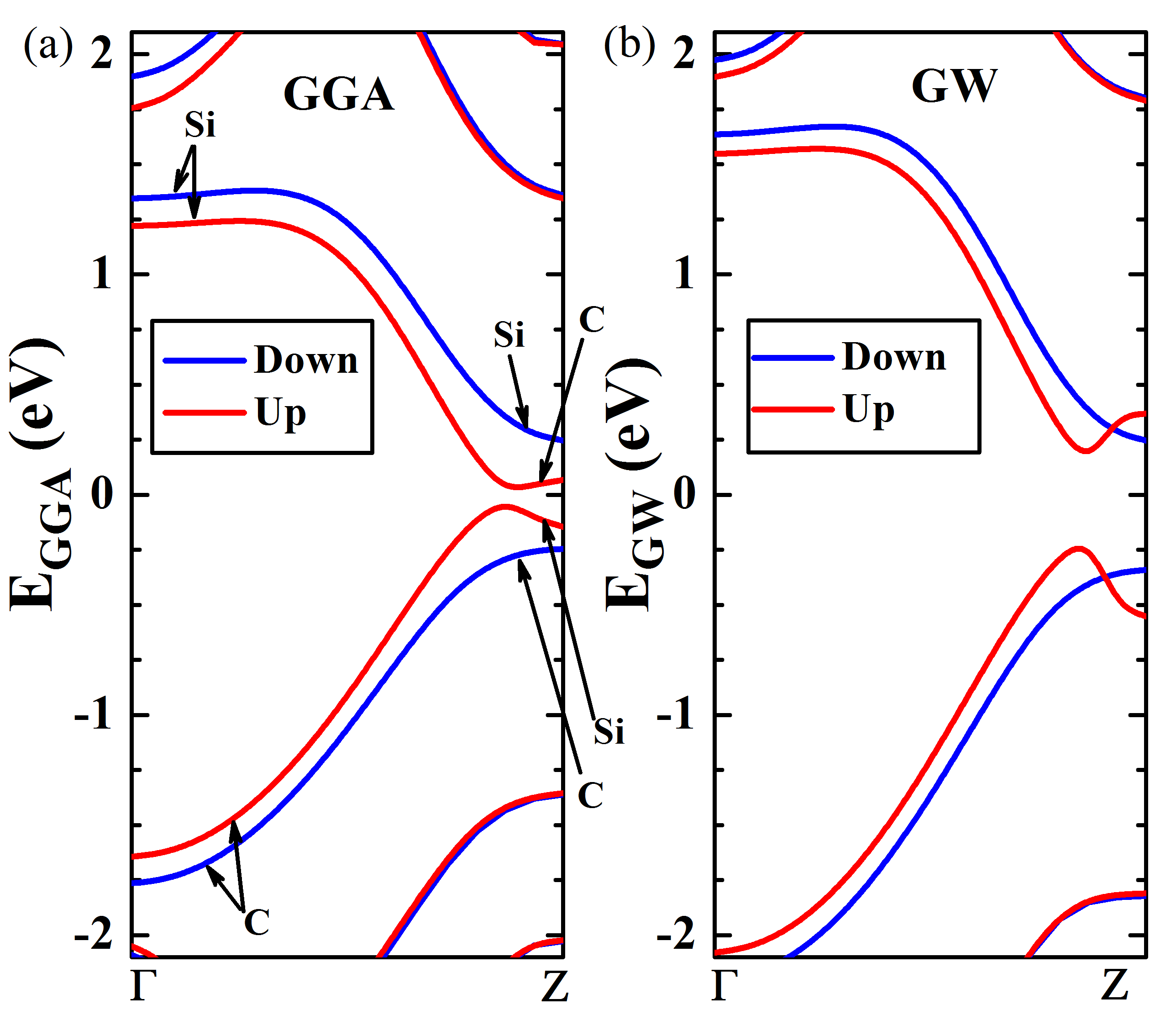
Next we present the results of quasiparticle band structure calculations of spin-polarized ZSiCNR-4, because to have similar band structures, and at mean-field DFT level exhibit intrinsic half-metallic behavior.21; 36 In Figs. 5 (a) and (b) we compare the GGA and GW quasiparticle band structures of ZSiCNR-4, and show the widened quasiparticle band gap, when electron-correlation effects are included. While DFT-GGA predicts a very small gap of 30 meV, the GW quasiparticle gap is seen to have widened to 0.33 eV, clearly showing that the ZSiCNRs are narrow-gap semiconductors (Table 1). Although, after including many-body effects through GW calculations, half-metallicity disappears, but still the band gaps for two spin orientations are different. The atoms contributing to various states are marked in Fig. 5 (a). Towards the zone boundary, the states of the first valence and conduction bands of both spins are localized at the ribbon edges.36 From the spin-density plot presented in Fig. 1 (b), it is obvious that the spins localized on the two edges have opposite spin orientations. The states to the left of the VBM/CBM extend over the entire ribbon width, except for the spin-down conduction band which mainly comprises of the Si edge states. The screening at the edges shows a complicated dependence on the states, which is enhanced in ZSiCNRs because the charge and spin distributions differ at the Si and C edges. Fig. 6 shows that the self energy corrections are highly state-dependent. The states which are enclosed in rectangular boxes, away from the main region, represent the spin-up edge states (valence states at the Si edge, and conduction states at the C edge). As the wave vector approaches the zone boundary (Z point), the states get more localized at the edges,62 and the deviations between up- and down-spin states, as also the energy gap for up-spin states, become larger (cf. Fig. 5(a)). Thus, the nature of spin-up bands is very similar to the bands in spin degenerate zigzag graphene nanoribbons.48
| spin-up | spin-down | |||||
|---|---|---|---|---|---|---|
| Nz | ||||||
| 4 | 0.03 | 0.33 | 0.30 | 0.55 | 0.59 | 0.04 |
| 5 | 0.06 | 0.82 | 0.76 | 0.72 | 0.77 | 0.05 |
| 6 | 0.006 | 0.38 | 0.37 | 0.64 | 0.74 | 0.1 |
| 7 | 0.002 | 0.384 | 0.38 | 0.64 | 0.92 | 0.28 |
| 8 | 0.08 | 0.77 | 0.69 | 0.76 | 0.93 | 0.14 |
The larger spin-down gap at the zone boundary exhibits a smaller quasi-particle correction. Fig. 6 shows the valence spin-down states bending away from the spin-up states, and, similarly, spin-down states of the conduction band too have smaller corrections than the corresponding spin-up states. These states correspond to the valence C, and the conduction Si, states localized at the edges. The spin-down edge states show smaller self energy corrections when compared to those localized in the interior, while the spin-up edge states exhibit exactly the opposite behavior. The charge distributions are different at the two edges, leading to varying amounts of screening. For example, in the ground state, there is a partial valence electron transfer from Si to C.63 As a consequence, the edge C states are screened more, and have smaller self energy corrections, while the lesser screened edge valence Si states experience enhanced Coulomb interactions. Therefore, the spin-down band gap does not change as much as the spin-up band gap.
A few points enclosed by dashed circles lying outside the main region are states. Apart from the first valence and conduction bands, the next few bands comprise both and states (shown in Fig. 6). Similar to ASiCNRs,52 and narrow ZSiCNRs, the states have smaller-self energy corrections than the states.
For the sake of completeness, we also performed calculations on the non-magnetic (i.e., non-spin polarized) states of ZSiCNRs, and found that spin polarized state does not exist for narrow ribbons (), and spin-polarized calculations for those ribbons yield the same results as non-magnetic calculations. However, for broader ribbons, both spin-polarized and non-magnetic states exist, and quite expectedly, total energies for the spin-polarized cases are lower as compared to the non-magnetic ones (see Table 2). We also performed GGA and GW calculations for the non-magnetic states of broader ribbons and results are presented in Table 3. From the table it is obvious that: (a) at DFT-GGA level band gaps of the ribbons decrease rapidly with their width, and (b) quasiparticle corrections are large for the ultra narrow ZSiCNRs, but they also reduce in magnitude rapidly with the increasing width. Combining these two results, we conclude that non-magnetic calculations predict that broader ZSiCNRs will exhibit metallic behavior. Therefore, an experimental measurement of the band gaps of broader ZSiCNRs can settle the issue whether these systems exhibit a magnetic ground state, or a nonmagnetic one.
| Nz | Total energy (eV) | (eV) | |
|---|---|---|---|
| NM | SP | ||
| 4 | -62.106675 | -62.115140 | 0.008465 |
| 5 | -76.101117 | -76.120842 | 0.019725 |
| 6 | -90.119364 | -90.144896 | 0.025532 |
| Nz | |||
|---|---|---|---|
| 2 | 0.97 | 2.4 | 1.43 |
| 3 | 0.07 | 0.45 | 0.36 |
| 4 | 0.011 | 0.22 | 0.209 |
| 5 | 0.015 | 0.15 | 0.135 |
| 6 | 0.002 | 0.07 | 0.068 |
We have not presented optical absorption spectra of spin-polarized ZSiCNRs as they undergo different quasiparticle self-energy corrections because of two spin band gaps. We could expect weakly bound excitons in ribbons that are wider than 1 nm. Small band gap of ZSiCNRs which are wider than 0.6 nm makes them potentially useful in IR devices.
IV Conclusions
We performed first-principles many-body calculations in order to investigate quasi particle band structures and optical absorption of hydrogen-passivated zigzag SiC nanoribbons whose widths ranged from 0.6 nm to 2.2 nm. For the study, computationally intensive GW approximation was employed to compute the self-energy corrected quasiparticle band gaps. We also used the BSE to calculate optical absorption spectra including eletron-hole effects. It was found that the many-body effects are significant due to the reduced dimensionality of nanoribbons. Self-energy corrections transformed nearly half-metallic zigzag SiC nanoribbons with width larger than 1 nm, to semiconductors. The inclusion of electron-hole effects changed optical absorption spectra in a significant manner, both qualitatively, and quantitatively. The excitonic binding energies and luminescence properties are dependent on width of the ribbon. We found that nanoribbon with a width of 0.6 nm has strongly bound excitons with binding energy of 2.1 eV, suggesting its possible utility in optoelectronic applications. We also computed the edge formation energy and showed that narrower ribbons are more stable when compared to wider ones. The unique Coulombic interactions at the spin-polarized edges make zigzag SiC nanoribbons interesting systems to study. As far as behavior of their band gaps with respect to the width is concerned, because the band gaps in half-metallic ZSiCNRs arise due to the presence of magnetic edge states, therefore, broader ribbons are expected to have spin-polarized non-zero band gaps, hinting at their possible utility in spintronic applications, such as spin valves.
Acknowledgements.
NA and NM gratefully acknowledge the support from Monash HPC, National Computing Infrastructure of Australia, and the Pawsey Supercomputing facility. This research was partially supported by the Australian Research Council Centre of Excellence in Future Low-Energy Electronics Technologies (project number CE170100039) and funded by the Australian Government. AS acknowledges the financial support from Department of Science and Technology, Government of India, under project no. SB/S2/CMP-066/2013.References
- Novoselov et al. (2004) K. S. Novoselov, A. K. Geim, S. V. Morozov, D. Jiang, Y. Zhang, S. V. Dubonos, I. V. Grigorieva, and A. A. Firsov, “Electric field effect in atomically thin carbon films,” Science 306, 666–669 (2004), http://www.sciencemag.org/content/306/5696/666.full.pdf .
- Geim and Novoselov (2007) Andre K Geim and Konstantin S Novoselov, “The rise of graphene,” Nature materials 6, 183–191 (2007).
- Katsnelson (2007) Mikhail I Katsnelson, “Graphene: carbon in two dimensions,” Materials today 10, 20–27 (2007).
- Castro Neto et al. (2009) A. H. Castro Neto, F. Guinea, N. M. R. Peres, K. S. Novoselov, and A. K. Geim, “The electronic properties of graphene,” Rev. Mod. Phys. 81, 109–162 (2009).
- Coleman et al. (2011) Jonathan N Coleman, Mustafa Lotya, Arlene O’Neill, Shane D Bergin, Paul J King, Umar Khan, Karen Young, Alexandre Gaucher, Sukanta De, Ronan J Smith, et al., “Two-dimensional nanosheets produced by liquid exfoliation of layered materials,” Science 331, 568–571 (2011).
- Mak et al. (2010) Kin Fai Mak, Changgu Lee, James Hone, Jie Shan, and Tony F Heinz, “Atomically thin mos 2: a new direct-gap semiconductor,” Physical Review Letters 105, 136805 (2010).
- Wang et al. (2012) Qing Hua Wang, Kourosh Kalantar-Zadeh, Andras Kis, Jonathan N Coleman, and Michael S Strano, “Electronics and optoelectronics of two-dimensional transition metal dichalcogenides,” Nature nanotechnology 7, 699–712 (2012).
- Liu et al. (2014) Han Liu, Adam T Neal, Zhen Zhu, Zhe Luo, Xianfan Xu, David Tománek, and Peide D Ye, “Phosphorene: An unexplored 2d semiconductor with a high hole mobility,” ACS Nano 8, 4033–4041 (2014).
- Xia et al. (2003) Y. Xia, P. Yang, Y. Sun, Y. Wu, B. Mayers, B. Gates, Y. Yin, F. Kim, and H. Yan, “One-dimensional nanostructures: Synthesis, characterization, and applications,” Advanced Materials 15, 353–389 (2003).
- Wang and Li (2006) Xun Wang and Yadong Li, “Solution-based synthetic strategies for 1-d nanostructures,” Inorganic Chemistry 45, 7522–7534 (2006), pMID: 16961337, http://dx.doi.org/10.1021/ic051885o .
- Kosynkin et al. (2009) Dmitry V Kosynkin, Amanda L Higginbotham, Alexander Sinitskii, Jay R Lomeda, Ayrat Dimiev, B Katherine Price, and James M Tour, “Longitudinal unzipping of carbon nanotubes to form graphene nanoribbons,” Nature 458, 872–876 (2009).
- Zeng et al. (2010) Haibo Zeng, Chunyi Zhi, Zhuhua Zhang, Xianlong Wei, Xuebin Wang, Wanlin Guo, Yoshio Bando, and Dmitri Golberg, ““white graphenes”: boron nitride nanoribbons via boron nitride nanotube unwrapping,” Nano letters 10, 5049–5055 (2010).
- Son et al. (2006a) Young-Woo Son, Marvin L. Cohen, and Steven G. Louie, “Energy gaps in graphene nanoribbons,” Phys. Rev. Lett. 97, 216803 (2006a).
- Ramasubramaniam (2010) Ashwin Ramasubramaniam, “Electronic structure of oxygen-terminated zigzag graphene nanoribbons: A hybrid density functional theory study,” Phys. Rev. B 81, 245413 (2010).
- Lee and Cho (2009) Geunsik Lee and Kyeongjae Cho, “Electronic structures of zigzag graphene nanoribbons with edge hydrogenation and oxidation,” Physical Review B 79, 165440 (2009).
- Son et al. (2006b) Young-Woo Son, Marvin L Cohen, and Steven G Louie, “Half-metallic graphene nanoribbons,” Nature 444, 347–349 (2006b).
- Lou (2013) Ping Lou, “Effects of edge hydrogenation in zigzag silicon carbide nanoribbons: stability, electronic and magnetic properties, as well as spin transport property,” J. Mater. Chem. C 1, 2996–3003 (2013).
- Harris (1995) Garry.L Harris, Properties of Silicon Carbide, 1st ed. (INSPEC, Institution of Electrical Engineers, London. United Kingdom, 1995).
- Ivanov and Chelnokov (1992) PA Ivanov and VE Chelnokov, “Recent developments in sic single-crystal electronics,” Semiconductor science and technology 7, 863 (1992).
- Lin et al. (2013) Xiao Lin, Shisheng Lin, Yang Xu, Ayaz Ali Hakro, Tawfique Hasan, Baile Zhang, Bin Yu, Jikui Luo, Erping Li, and Hongsheng Chen, “Ab initio study of electronic and optical behavior of two-dimensional silicon carbide,” Journal of Materials Chemistry C 1, 2131–2135 (2013).
- Sun et al. (2008) Lian Sun, Yafei Li, Zhenyu Li, Qunxiang Li, Zhen Zhou, Zhongfang Chen, Jinlong Yang, and JG Hou, “Electronic structures of sic nanoribbons,” The Journal of chemical physics 129, 174114 (2008).
- Bekaroglu et al. (2010) E. Bekaroglu, M. Topsakal, S. Cahangirov, and S. Ciraci, “First-principles study of defects and adatoms in silicon carbide honeycomb structures,” Phys. Rev. B 81, 075433 (2010).
- Lu et al. (2012) Tie-Yu Lu, Xia-Xia Liao, Hui-Qiong Wang, and Jin-Cheng Zheng, “Tuning the indirect-direct band gap transition of sic, gec and snc monolayer in a graphene-like honeycomb structure by strain engineering: a quasiparticle gw study,” J. Mater. Chem. 22, 10062–10068 (2012).
- Ding and Wang (2013) Yi Ding and Yanli Wang, “Density functional theory study of the silicene-like six and xsi3 (x = b, c, n, al, p) honeycomb lattices: The various buckled structures and versatile electronic properties,” The Journal of Physical Chemistry C 117, 18266–18278 (2013).
- Hsueh et al. (2011) H. C. Hsueh, G. Y. Guo, and Steven G. Louie, “Excitonic effects in the optical properties of a sic sheet and nanotubes,” Phys. Rev. B 84, 085404 (2011).
- Baumeier et al. (2007) Björn Baumeier, Peter Krüger, and Johannes Pollmann, “Structural, elastic, and electronic properties of sic, bn, and beo nanotubes,” Phys. Rev. B 76, 085407 (2007).
- Şahin et al. (2009) H. Şahin, S. Cahangirov, M. Topsakal, E. Bekaroglu, E. Akturk, R. T. Senger, and S. Ciraci, “Monolayer honeycomb structures of group-iv elements and iii-v binary compounds: First-principles calculations,” Phys. Rev. B 80, 155453 (2009).
- Wu and Guo (2007) I. J. Wu and G. Y. Guo, “Optical properties of nanotubes: An ab initio study,” Phys. Rev. B 76, 035343 (2007).
- Zhao et al. (2010) Kun Zhao, Mingwen Zhao, Zhenhai Wang, and Yingcai Fan, “Tight-binding model for the electronic structures of sic and {BN} nanoribbons,” Physica E: Low-dimensional Systems and Nanostructures 43, 440 – 445 (2010).
- Lin (2012) S. S. Lin, “Light-emitting two-dimensional ultrathin silicon carbide,” The Journal of Physical Chemistry C 116, 3951–3955 (2012), http://pubs.acs.org/doi/pdf/10.1021/jp210536m .
- Sun et al. (2002) Xu-Hui Sun, Chi-Pui Li, Wing-Kwong Wong, Ning-Bew Wong, Chun-Sing Lee, Shuit-Tong Lee, and Boon-Keng Teo, “Formation of silicon carbide nanotubes and nanowires via reaction of silicon (from disproportionation of silicon monoxide) with carbon nanotubes,” Journal of the American Chemical Society 124, 14464–14471 (2002).
- Yushin et al. (2008) Gleb N. Yushin, Z. Goknur Cambaz, Yury Gogotsi, Kateryna L. Vyshnyakova, and Lyudmila N. Pereselentseva, “Carbothermal synthesis of -sic micro-ribbons,” Journal of the American Ceramic Society 91, 83–87 (2008).
- Xi et al. (2004) Guangcheng Xi, Yiya Peng, Songming Wan, Tanwei Li, Weichao Yu, and Yitai Qian, “Lithium-assisted synthesis and characterization of crystalline 3c-sic nanobelts,” The Journal of Physical Chemistry B 108, 20102–20104 (2004).
- Wu et al. (2007) Renbing Wu, Lingling Wu, Guangyi Yang, Yi Pan, Jianjun Chen, Rui Zhai, and Jing Lin, “Fabrication and photoluminescence of bicrystalline sic nanobelts,” Journal of Physics D: Applied Physics 40, 3697 (2007).
- Zhang et al. (2010a) Huan Zhang, Weiqiang Ding, Kai He, and Ming Li, “Synthesis and characterization of crystalline silicon carbide nanoribbons,” Nanoscale research letters 5, 1264–1271 (2010a).
- Lou and Lee (2009a) Ping Lou and Jin Yong Lee, “Band structures of narrow zigzag silicon carbon nanoribbons,” The Journal of Physical Chemistry C 113, 12637–12640 (2009a), http://pubs.acs.org/doi/pdf/10.1021/jp903155r .
- Lou and Lee (2009b) Ping Lou and Jin Yong Lee, “Electrical control of magnetization in narrow zigzag silicon carbon nanoribbons,” The Journal of Physical Chemistry C 113, 21213–21217 (2009b), http://pubs.acs.org/doi/pdf/10.1021/jp906558y .
- Ding and Wang (2012) Yi Ding and Yanli Wang, “Electronic structures of zigzag sic nanoribbons with asymmetric hydrogen-terminations,” Applied Physics Letters 101, 013102 (2012).
- Lopez-Bezanilla et al. (2013) Alejandro Lopez-Bezanilla, Jingsong Huang, Paul R. C. Kent, and Bobby G. Sumpter, “Tuning from half-metallic to semiconducting behavior in sic nanoribbons,” The Journal of Physical Chemistry C 117, 15447–15455 (2013), http://dx.doi.org/10.1021/jp406547a .
- Zheng et al. (2011) Fang-Ling Zheng, Yan Zhang, Jian-Min Zhang, and Ke-Wei Xu, “Bandgap modulations of silicon carbon nanoribbons by transverse electric fields: A theoretical study,” physica status solidi (b) 248, 1676–1681 (2011).
- Costa and Morbec (2011) CD Costa and JM Morbec, “Boron and nitrogen impurities in sic nanoribbons: an ab initio investigation,” Journal of Physics: Condensed Matter 23, 205504 (2011).
- Tang et al. (2013) Zhen-Kun Tang, Ling-Ling Wang, Li-Ming Tang, Wei-Qing Huang, Deng-Yu Zhang, Liang Xu, and Xiao-Fei Li, “Electronic and magnetism properties of half-bare zigzag silicon carbon nanoribbons from hybrid density functional calculations,” Solid State Communications 158, 25 – 28 (2013).
- Morbec and Rahman (2013) Juliana M. Morbec and Gul Rahman, “Role of vacancies in the magnetic and electronic properties of sic nanoribbons: An ab initio study,” Phys. Rev. B 87, 115428 (2013).
- Lou (2014) Ping Lou, “Short-range exact exchange effects in ultra-narrow zigzag silicon carbide nanoribbons,” physica status solidi (b) 251, 423–434 (2014).
- Godby et al. (1986) R. W. Godby, M. Schlüter, and L. J. Sham, “Accurate exchange-correlation potential for silicon and its discontinuity on addition of an electron,” Phys. Rev. Lett. 56, 2415–2418 (1986).
- Prezzi et al. (2008) Deborah Prezzi, Daniele Varsano, Alice Ruini, Andrea Marini, and Elisa Molinari, “Optical properties of graphene nanoribbons: The role of many-body effects,” Phys. Rev. B 77, 041404 (2008).
- Yang et al. (2007) Li Yang, Marvin L. Cohen, and Steven G. Louie, “Excitonic effects in the optical spectra of graphene nanoribbons,” Nano Letters 7, 3112–3115 (2007), http://pubs.acs.org/doi/pdf/10.1021/nl0716404 .
- Yang et al. (2008) Li Yang, Marvin L. Cohen, and Steven G. Louie, “Magnetic edge-state excitons in zigzag graphene nanoribbons,” Phys. Rev. Lett. 101, 186401 (2008).
- Wang et al. (2011) Shudong Wang, Qian Chen, and Jinlan Wang, “Optical properties of boron nitride nanoribbons: Excitonic effects,” Applied Physics Letters 99, 063114 (2011).
- Hu et al. (2012) Chunping Hu, Ryo Ogura, Nobuhito Onoda, Satoru Konabe, and Kazuyuki Watanabe, “Quasiparticle band gaps of boron nitride nanoribbons,” Phys. Rev. B 85, 245420 (2012).
- Kim et al. (2015) Jongmin Kim, Won Seok Yun, and J. D. Lee, “Optical absorption of armchair mos2 nanoribbons: Enhanced correlation effects in the reduced dimension,” The Journal of Physical Chemistry C 119, 13901–13906 (2015), http://dx.doi.org/10.1021/acs.jpcc.5b02232 .
- Alaal et al. (2016) Naresh Alaal, Vaideesh Loganathan, Nikhil Medhekar, and Alok Shukla, “First principles many-body calculations of electronic structure and optical properties of sic nanoribbons,” Journal of Physics D: Applied Physics 49, 105306 (2016).
- Fuchs and Scheffler (1999a) Martin Fuchs and Matthias Scheffler, “Ab initio pseudopotentials for electronic structure calculations of poly-atomic systems using density-functional theory,” Computer Physics Communications 119, 67–98 (1999a).
- Fuchs and Scheffler (1999b) Martin Fuchs and Matthias Scheffler, “Ab initio pseudopotentials for electronic structure calculations of poly-atomic systems using density-functional theory,” Computer Physics Communications 119, 67–98 (1999b).
- Kresse and Furthmüller (1996) G. Kresse and J. Furthmüller, “Efficiency of ab-initio total energy calculations for metals and semiconductors using a plane-wave basis set,” Computational Materials Science 6, 15 – 50 (1996).
- Gonze et al. (2009) X. Gonze, B. Amadon, P.-M. Anglade, J.-M. Beuken, F. Bottin, P. Boulanger, F. Bruneval, D. Caliste, R. Caracas, M. Côté, T. Deutsch, L. Genovese, Ph. Ghosez, M. Giantomassi, S. Goedecker, D.R. Hamann, P. Hermet, F. Jollet, G. Jomard, S. Leroux, M. Mancini, S. Mazevet, M.J.T. Oliveira, G. Onida, Y. Pouillon, T. Rangel, G.-M. Rignanese, D. Sangalli, R. Shaltaf, M. Torrent, M.J. Verstraete, G. Zerah, and J.W. Zwanziger, “Abinit: First-principles approach to material and nanosystem properties,” Computer Physics Communications 180, 2582 – 2615 (2009).
- Gonze (2005) Xavier Gonze, “A brief introduction to the abinit software package,” Zeitschrift für Kristallographie 220, 558–562 (2005).
- Onida et al. (2002) Giovanni Onida, Lucia Reining, and Angel Rubio, “Electronic excitations: density-functional versus many-body green’s-function approaches,” Rev. Mod. Phys. 74, 601–659 (2002).
- Godby and Needs (1989) R. W. Godby and R. J. Needs, “Metal-insulator transition in kohn-sham theory and quasiparticle theory,” Phys. Rev. Lett. 62, 1169–1172 (1989).
- Fetter and Walecka (1971) Alexander L. Fetter and John D. Walecka, Quatum theory of many-particle systems, 1st ed. (Mcgraw-Hill, New York, 1971).
- Denk et al. (2014) Richard Denk, Michael Hohage, Peter Zeppenfeld, Jinming Cai, Carlo A Pignedoli, Hajo Söde, Roman Fasel, Xinliang Feng, Klaus Müllen, Shudong Wang, et al., “Exciton-dominated optical response of ultra-narrow graphene nanoribbons,” Nature communications 5, 4253 (2014).
- Fujita et al. (1996) Mitsutaka Fujita, Katsunori Wakabayashi, Kyoko Nakada, and Koichi Kusakabe, “Peculiar localized state at zigzag graphite edge,” Journal of the Physical Society of Japan 65, 1920–1923 (1996).
- Zhang et al. (2010b) Jian-Min Zhang, Fang-Ling Zheng, Yan Zhang, and Vincent Ji, “First-principles study on electronic properties of sic nanoribbon,” Journal of materials science 45, 3259–3265 (2010b).