Subnanosecond Time-to-Digital Converter Implemented in a Kintex-7 FPGA
Abstract
Time-to-digital converters (TDCs) are used in various fields, including high-energy physics. One advantage of implementing TDCs in field-programmable gate arrays (FPGAs) is the flexibility on the modification of the logics, which is useful to cope with the changes in the experimental conditions. Recent FPGAs make it possible to implement TDCs with a time resolution less than 10 ps. On the other hand, various drift chambers require a time resolution of (0.1) ns, and a simple and easy-to-implement TDC is useful for a robust operation. Herein an eight-channel TDC with a variable bin size down to 0.28 ns is implemented in a Xilinx Kintex-7 FPGA and tested. The TDC is based on a multisampling scheme with quad phase clocks synchronised with an external reference clock. Calibration of the bin size is unnecessary if a stable reference clock is available, which is common in high-energy physics experiments. Depending on the channel, the standard deviation of the differential nonlinearity for a 0.28 ns bin size is 0.13–0.31. The performance has a negligible dependence on the temperature. The power consumption and the potential to extend the number of channels are also discussed.
keywords:
Time-to-Digital Converter, Field-Programmable Gate Array1 Introduction
Time-to-digital converters (TDCs) are used in various fields, including high-energy physics. For example, in the ATLAS experiment [1], the muon momentum is measured with monitored drift tube (MDT) chambers based on TDCs with a bin size of 0.78 ns [2]. They are implemented in application-specific integrated circuits.
Recent moderate field-programmable gate arrays (FPGAs) make it possible to implement TDCs with a nanosecond or smaller bin size [3, 4]. Implementation of TDCs in FPGAs provides the flexibility to deal with the changes in the experimental conditions. The present TDC for the MDT chambers includes a transmitter with fixed bandwidth of 80 Mbit/s and has limitations on the readout for increased luminosity [5]. On the other hand, FPGAs can in general manage the bandwidth change. In addition to the flexibility, FPGAs have advantages on the availability of highly reliable circuits, e.g. the clock managers and the data transceivers [6, 7].
In this study, an eight-channel TDC with a variable bin size down to 0.28 ns is implemented in a Xilinx Kintex-7 FPGA [8] and tested. The type of the employed FPGA is XC7K325T-2FFG900, where the speed grade is -2. The TDC is based on multi-phase clocks managed by a highly reliable clock manager integrated in the FPGA. Calibration of the bin size is unnecessary if a stable reference clock is available, which is common in high-energy physics experiments. The logic is simple and easy-to-implement.
This study extends the demonstration described in [9] by further analysing and interpreting the data as well as measuring the power consumption. Additionally, the potential to extend the number of channels to 256 is discussed. This study does not include the measurements of the radiation tolerance of the FPGA, for which some results are available in [10].
2 Design of the TDC
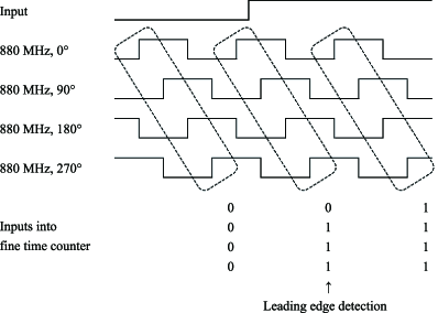
Figure 1 shows a block diagram of the TDC. It is based on a multisampling scheme with quad phase clocks [11, 12, 13]. The input signal is divided into four, and detected by four D-type flip-flops. The outputs from the D-type flip-flops are aligned step by step in the chains of additional D-type flip-flops, where the metastable states are suppressed. From the pattern of the outputs from the chains, a three-bit fine time count is provided. The timing of both the leading and trailing edges is extracted. Figure 2 shows a timing chart of an example input signal and the quad phase clocks.
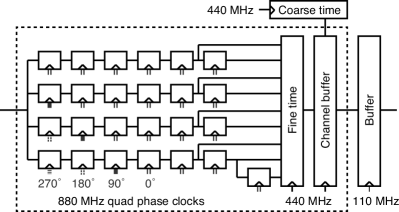
The three-bit time count and a one-bit identifier of the leading and trailing edges are combined with the data from a fourteen-bit coarse time counter, and stored in a channel buffer. The channel buffers for all channels are scanned, and the data is transferred to a buffer. A three-bit channel identifier is attached. There is no selection on the data by the trigger, and all the data are simply read out one by one.
The difference in the lengths of the divided input signal paths (see Figure 1) is crucial for the TDC performance. The locations of the first four D-type flip-flops in each channel are constrained so that they are close to each other.
The quad phase clocks are produced by the clock manager of the Kintex-7 FPGA. They are synchronised with the external reference clock. The maximum clock frequency supported for the FPGA employed in this study is 933 MHz. The quad phase clock frequency and the TDC bin size can be varied by changing the external reference clock frequency. An external reference clock with a 110 MHz frequency corresponds to that of the quad phase clocks of 880 MHz and a bin size of 0.28 ns.
The dynamic range for a bin size of 0.28 ns is 37 s. The dynamic range can be extended by changing the number of bits for the coarse time counter. A minimal latency from the signal input to the buffer output is 0.21 s, while the latency depends on the rate of the signal input.
3 Demonstrator and Test Setup
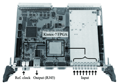
Figure 3 shows a picture of the demonstrator, which consists of a motherboard and a daughter card. The motherboard is compatible with the versatile backplane bus standard VME [14]. It has a Kintex-7 FPGA (type is XC7K325T-2FFG900). The system clock is provided from a LEMO coaxial connector [15]. The output from the FPGA is read through a gigabit Ethernet with a Transmission Control Protocol processor implemented in the FPGA (SiTCP) [16]. The daughter card has eight LEMO coaxial connectors as signal inputs. The input compatible with the NIM fast negative signal [17] is converted into a 3.3 V LVCMOS signal [18] with Texas Instruments SN65LVDS348PW [19], and transferred to the FPGA on the motherboard.
The signal and external reference clocks are from the pulse generator Agilent 81150A [20]. The standard deviation of the time difference between the leading edges of the two synchronised pulses from the pulse generator is 30 ps. The performances of bin sizes of 0.78 ns, 0.39 ns, and 0.28 ns, which correspond to the external reference clock frequencies of 40 MHz, 80 MHz, and 110 MHz, respectively, were evaluated. Unless otherwise specified, the results for the 0.28-ns bin size are shown. Although the leading edges were evaluated, the trailing edges should produce similar results since common clocks and D-type flip-flops are used.
4 Differential Nonlinearity
The differential nonlinearity is defined by
| (1) |
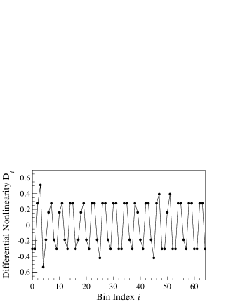
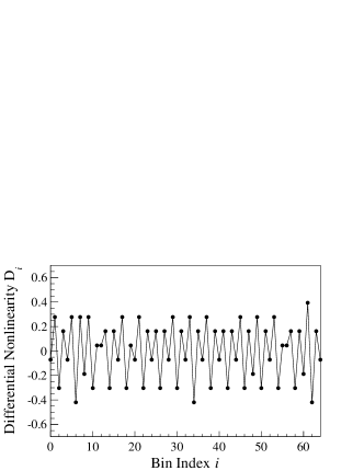
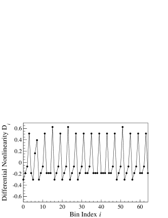
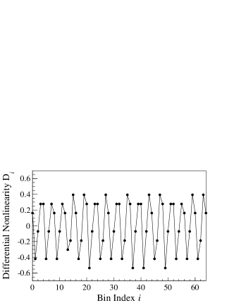
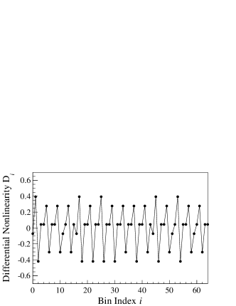
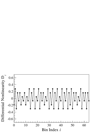
where () is the bin index, is the bin size for bin , and is the designed bin size. To evaluate , the time difference of the leading edges between the signal and external reference clocks was measured. Multiple bins were investigated by scanning the time difference between the signal and external reference clocks with a 33-ps step size (Figure 4). A periodic structure with a cycle of four bins was found. The maximum magnitude of the measured is 0.6.

The delay before the first D-type flip-flop for each divided input signal path () was estimated by a Xilinx Vivado design tool. Based on the estimated delay, the bin size for each quad clock phase was calculated as
| (2) |
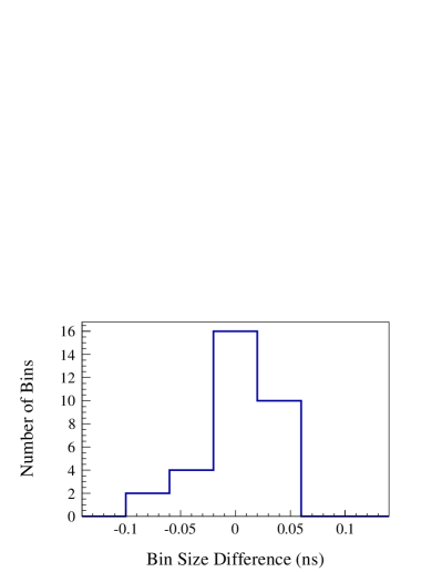
A cyclic relation of was used to calculate . Table 1 shows the measured and calculated bin sizes for a channel. Figure 5 shows the distribution of the difference between the measured and calculated bin sizes for all 32 quad clock phases of the 8 channels. The difference is O(0.01) ns, implying that the main source of the periodic structure in Figure 4 is the difference in the divided input signal paths.
| Phase | Input signal | Calculated | Measured |
|---|---|---|---|
| delay [ns] | bin size [ns] | bin size [ns] | |
| 0 | 4.62 | 0.20 | 0.21 |
| 1 | 4.70 | 0.20 | 0.20 |
| 2 | 4.79 | 0.34 | 0.36 |
| 3 | 4.73 | 0.39 | 0.37 |
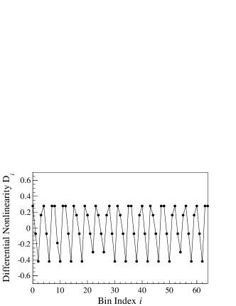
As a channel-level measure of , the deviation is defined for each channel by
| (3) |
where is the total number of bins. Figure 6 shows the result of the measurement of . The obtained value, which varies between 0.13–0.31, depends on the channel.

5 Integral Nonlinearity
The integral nonlinearity is given by
| (4) |
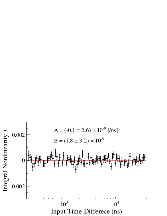
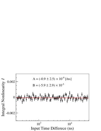
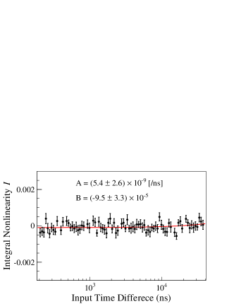
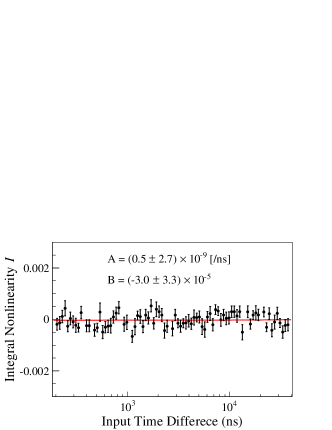
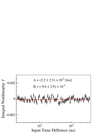
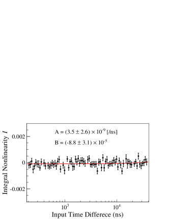
where is the time difference between the leading edges of the input signal clock and is the mean of the measurements. The time difference was scanned up to 37 s, and is obtained for each time difference. The graph is fitted by a linear function . The fit result is shown in Figure 7. The deviation between the slope parameter and zero is at most , where the uncertainty of is only 1 ps over 37 s. The magnitude of the mean of the offset parameter is at most , which corresponds to an offset of only 0.03 ps.


6 Time Resolution
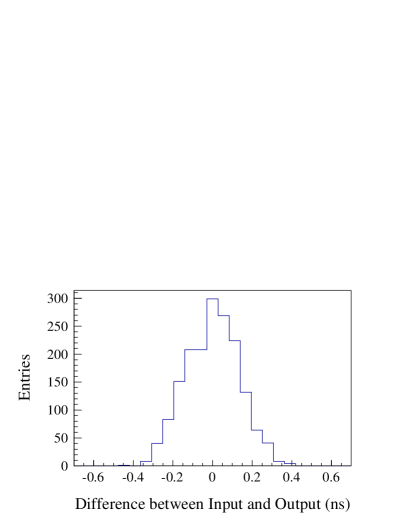
The time resolution was evaluated from the measurement of the time difference between the neighbouring leading edges of the input signal clock. The cycle of the input signal clock was scanned from 200 ns to 37 s. Figure 8 shows the difference between the measured and input time difference. Figure 9 shows the standard deviation of the difference for each channel. The standard deviation is considered to be the time resolution. The obtained time resolution depends on the channel and ranges 0.08–0.10 ns. The linear correlation factor between the time resolution and the deviation shown in Figure 6 is 0.9. This result indicates that the time resolution depends on the difference between the input signal paths.
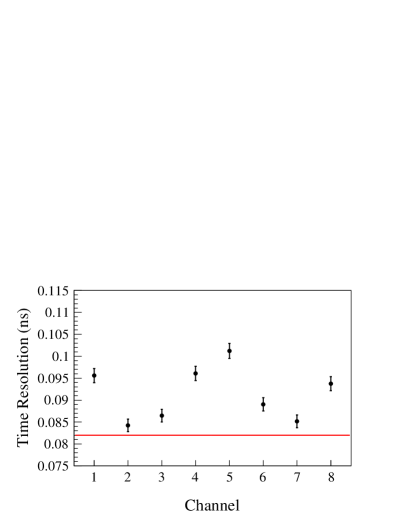
For a bin size of 0.28 ns, the time resolution is larger than the quantisation error as shown in Figure 9. The difference between the input signal paths has no dependence on the bin size. On the other hand, the quantisation error has a linear relation with the bin size. Therefore, the time resolution is closer to the quantisation error for larger bin sizes. As an example, for a bin size of 0.78 ns, the measured time resolution was 0.23 ns for most channels.
7 Temperature Dependence
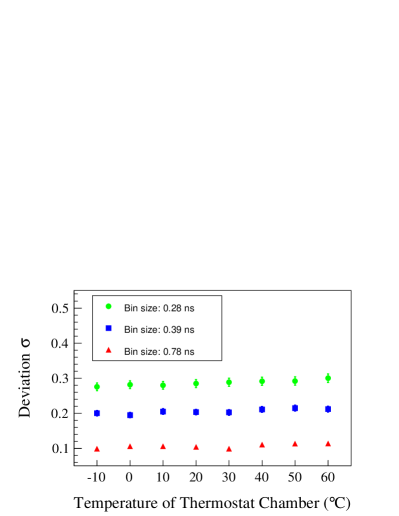
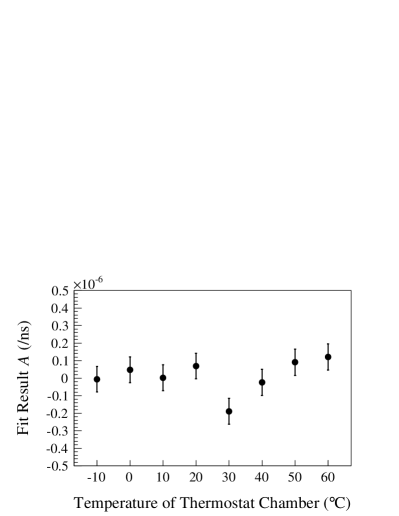
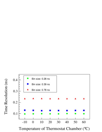
The temperature dependences of , , and the time resolution were evaluated with a thermostat chamber ESPEC SH-641 [21] for a range of the chamber temperature from C to C. The data were acquired after the temperature of FPGA became stable during the operation. The temperature of FPGA during operation was about 8 ∘C higher than that of the chamber. Figure 10 shows the relation between the deviation of and the temperature. Figure 11 shows the relation between the slope parameter from the linear fit to and the temperature. Figure 12 shows the relation between the time resolution and the temperature. The temperature dependence is small in the investigated temperature range.
8 Power Consumption
The power consumption of FPGA for the eight-channel TDC was estimated by the Vivado design tool. Table 2 summarises the results on the FPGA temperature of 28 ∘C and 68 ∘C for bin sizes of 0.28 ns and 0.78 ns. Since the temperature of the FPGA during the measurement was 8 ∘C higher than that of the thermostat chamber, we took 28 ∘C and 68 ∘C as the references. The dominant contributors for the dynamic power consumption are found to be the clock manager and SiTCP, which spend about 40% and 30%, respectively. Assuming a linear relation between the number of channels and the power consumption, the power consumption per channel for the bin sizes of 0.28 ns and 0.78 ns is 0.02 W and 0.01 W, respectively.
| Bin size | FPGA temperature | Dynamic | Static | Total |
|---|---|---|---|---|
| [∘C] | [W] | [W] | [W] | |
| 0.28 | 28 | 0.56 | 0.18 | 0.73 |
| 0.28 | 68 | 0.56 | 0.59 | 1.15 |
| 0.78 | 28 | 0.43 | 0.18 | 0.61 |
| 0.78 | 68 | 0.43 | 0.59 | 1.02 |
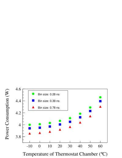
Figure 13 shows the measured power consumption of the demonstrator. The measured power consumption for the 0.28-ns bin size at a chamber temperature 20 ∘C is 4.1 W. The static power consumption of the demonstrator for the same bin size and the same temperature measured without firmware implemented in FPGA is 2.0 W. The dynamic power consumption of Texas Instruments DP83865DVH [19] for Ethernet data transfer, which is considered the main consumer on the demonstrator other than FPGA, is estimated to be 1.3 W. The value of is close to the value estimated from the Vivado design tool of 0.73 W.
9 Resources and Number of Channels
Table 3 summarises the utilisation of the FPGA resources for the tested eight-channel TDC. Because multiple clocks with different frequencies are generated, the ratio of the utilised clocking resources to the total clocking resources is relatively large. Most of the resources of the look-up tables, the registers, and the random-access memory are spent by SiTCP.
| Resource | Utilised | Available | Ratio [%] |
|---|---|---|---|
| Look-up tables | 4361 | 203800 | 2.1 |
| Registers | 5939 | 407600 | 1.5 |
| Memory | 48 | 445 | 10.8 |
| Input/output ports | 60 | 582 | 10.3 |
| Clocking | 14 | 32 | 43.8 |
We developed firmware with 256 channels to discuss the potential extension of the number of channels. Table 4 shows the utilised resources. The ratio of the utilised input/output ports to the total input/output ports is 58%, while the ratios for the other elements are smaller. The difference in the divided input signal delay for each channel was evaluated by the Vivado design tool. The standard deviation of the input signal delay is 0.14 ns. The clock skew may affect the offset between the channels, but it is within a range supported for the employed Kintex-7 FPGA.
| Resource | Utilised | Available | Ratio [%] |
|---|---|---|---|
| Look-up tables | 27682 | 203800 | 13.6 |
| Registers | 48826 | 407600 | 12.0 |
| Memory | 180 | 445 | 40.4 |
| Input/output ports | 292 | 582 | 58.4 |
| Clocking | 14 | 32 | 43.8 |
10 Conclusion
An eight-channel TDC with a variable bin size down to 0.28 ns was implemented in a Xilinx Kintex-7 FPGA (XC7K325T-2FFG900) and tested. The TDC is based on a multisampling scheme with quad phase clocks synchronised with an external reference clock. The measured time resolution for a 0.28-ns bin size is 0.08–0.10 ns, depending on the channel. The performance has a negligible dependence on the temperature. Although the actual performance was not demonstrated, it is possible to provide the firmware of a 256-channel TDC in a Xilinx design tool with a 0.14 ns standard deviation of the input signal delay.
Implementation of TDCs in FPGAs increases the flexibility to modify logics. This feature is advantageous when coping with the changes in the experimental conditions. If a stable reference clock is available such as in high-energy physics experiments, the TDC in this study does not need to be calibrated. In addition to the flexibility, FPGAs have advantages on the availability of various highly reliable circuits, e.g. clock managers and data transceivers. Consequently, the FPGA-based TDCs are useful in fields requiring subnanosecond resolution and simple and robust operation.
Acknowledgements
We acknowledge the support of the demonstrator developers Hiroshi Sakamoto, Chikuma Kato, Takayuki Tokunaga, and Yusaku Urano, at The University of Tokyo, Tokyo, Japan. We are also grateful for the support from the Open-It Consortium.
References
- [1] G. Aad et al. (ATLAS Collaboration), The ATLAS Experiment at the CERN Large Hadron Collider, 2008 JINST 3 S08003.
- [2] Y. Arai et al., ATLAS Muon Drift Tube Electronics, 2008 JINST 3 P09001.
- [3] T. Uchida et al., Readout Electronics for the Central Drift Chamber of the Belle-II Detector, IEEE Trans. Nucl. Sci., 62 (4), pp. 1741–1746.
- [4] C. Liu and Y. Wang, A 128-Channel, 710 M Samples/Second, and Less Than 10 ps RMS Resolution Time-to-Digital Converter Implemented in a Kintex-7 FPGA, IEEE Trans. Nucl. Sci., 62 (3), pp. 773–783.
- [5] ATLAS Collaboration, ATLAS Phase-II Upgrade Scoping Document, CERN-LHCC-2015-020; LHCC-G-166.
- [6] Xilinx Inc., 7 Series FPGAs Data Sheet: Overview, DS180 (v2.4), http://www.xilinx.com/
- [7] Microsemi Corp., IGLOO2 FPGA and SmartFusion2 SoC FPGA Datasheet, DS0128, Revision 11.0, https://www.microsemi.com/
- [8] Xilinx Inc., Kintex-7 FPGAs Data Sheet: DC and AC Switching Characteristics, DS182 (v2.16), http://www.xilinx.com/
- [9] Y. Sano et al., Development of a Sub-Nanosecond Time-to-Digital Converter Based on a Field-Programmable Gate Array, 2016 JINST 11 C03053.
- [10] Xilinx Inc., Device Reliability Report, UG116 (v10.6.1), http://www.xilinx.com/
- [11] M. D. Fries and J. J. Williams, High-Precision TDC in an FPGA Using a 192-MHz Quadrature Clock, in: Proc. IEEE NSS, 2012, pp. 580–584.
- [12] D. F. Spencer, J. Cole, M. Drigert, and R. Aryaeinejad, A High-Resolution, Multi-Stop, Time-to-Digital Converter for Nuclear Time-of-Flight Measurements, Nucl. Instrum. Methods Phys. Res. A. 556(1), pp. 291–295.
- [13] J. Wu, S. Hansen, and Z. Shi, ADC and TDC Implemented Using FPGA, in: Proc. IEEE NSS, 2007, pp. 281–286.
- [14] IEEE Standard for A Versatile Backplane Bus: VMEbus, IEEE Standard 1014-1987.
- [15] LEMO S.A., http://www.lemo.com/
- [16] T. Uchida, Hardware-Based TCP Processor for Gigabit Ethernet, IEEE Trans. Nucl. Sci., 55 (3), pp. 1631–1637.
- [17] Standard NIM Instrumentation System, DOE/ER-0457T; DE90010387.
- [18] Interface Standard for Nominal 3.0 V/3.3 V Supply Digital Integrated Circuits, JEDEC Standard JESD8C.01.
- [19] Texas Instruments Inc., http://www.ti.com/
- [20] Agilent Technologies Inc., http://www.agilent.com/
- [21] ESPEC Corp., http://www.espec-global.com/