Plasmons in one and two dimensions
H. Pfnür∗11footnotemark: 1, C. Tegenkamp∗, and L. Vattuone∗∗
∗ Institut für Festkörperphysik, Abt. ATMOS, Leibniz Universität
Hannover, Appelstr. 2,
D-30167 Hannover, Germany
∗∗ Dipartimento di Fisica, Università di Genova, Via Dodecaneso 33, IT-16146,
Genova, Italy
1 Introduction
The long-range Coulomb interaction between valence electrons in metals results in collective plasma oscillations, as pointed out already by Pines and Bohm [1, 2] as early as 1952. Plasmons exist in all dimensions [3]. The surface as the typical truncation of a bulk materials imposes a new boundary condition on these collective plasma oscillations resulting in localized states at the surface, called surface plasmons [4, 5]. In other words, the surface plasmon is the edge plasmon of a three-dimensional metal. Surface plasmons have a finite frequency in the long wavelength limit, which for a nearly free electron gas is located at with the bulk plasmon frequency, and a small dispersion with either positive or negative slope depending on the screening properties of the participating electronic orbitals [6, 7]. These properties of the surface plasmon also allow direct crossing of the surface plasmon dispersion with the light line and thus the direct interaction with light. The combined excitation of a surface plasmon in presence of electromagnetic radiation is called a surface plasmon-polariton (SPP), which represents the basis for the rapidly growing field of nanoplasmonics, opening the route for surface plasmon subwavelength optics [8], surface plasmon enhanced spectroscopy [9] near field optics [10] and chemical applications [11, 12].
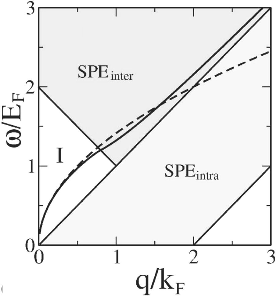
In this contribution, however, we will deal primarily with a different kind of collective low-energy excitations, generated in low-dimensional electron gases in one (1D) and two dimensions (2D). Most prominent examples are the 2D sheet plasmons of a metallic monolayer that were observed, e.g., in Ag or Dy monolayers on Si(111) [13, 14], in monolayers of graphene on SiC or metal surfaces [15], but also the 2D plasmons of partially filled surface states found on the clean surfaces of Be(0001) [16, 17], Cu(111) [18, 19] and Au(111)[20, 21], which result in so-called acoustic surface plasmons (ASP). Their relevance has two aspects: It is worthwhile to study the specifics of plasmonic excitations in low-dimensional systems in more detail, since both partial localization and correlations are important [7]. Therefore, a quantitative theory for plasmonic excitations going beyond the nearly-free electron gas model (NFEG) [22] is highly desirable. Secondly, much higher in-plane confinements of excitations can be achieved with plasmons associated with a 2D electron gas, since their dispersion is much flatter than that of SPP, which allows for extraordinary confinement of energy from subterahertz to midinfrared frequencies by use of appropriate nanostructures providing the necessary momentum transfer. The - dependence of dispersion, however, makes a distortionless propagation of nonmonochromatic signals inherently impossible, since the different frequencies components propagate at different velocities. This drawback can be overcome by use of systems that have a linear rather than a square root dispersion. As we will illustrate below, a linear dependence of dispersion is always expected for low-D plasmons that are coupled and shielded by other 2D or 3D electron gases [23, 24]. This is, in particular, the case for metal surfaces supporting an electronic Shockley surface state (SS) with band dispersion crossing the Fermi level [25], which leads to the formation of the ASP .
The physics of experimentally accessible systems that exhibit quasi-1D properties are still largely unexplored. The most obvious reason is their inherent instability, which allows their existence as isolated systems only at K. 1D properties can, however, be stabilized if embedded into a 2D or 3D environment. The interaction with these environments not only stabilizes these systems, their feedback on 1D properties opens a wide range of variability and allows to manipulate them. Thus a variety of exotic phenomena such as charge and spin density waves becomes accessible and makes them quite interesting objects to be studied [26, 27]. In this context, the arrays of atomic wires generated by self-assembly on semiconducting surfaces [28, 29, 30, 31, 32] are particularly attractive: they are not only geometricallystrongly anisotropic [29, 33, 34], but they also exhibit quasi-1D Fermi surfaces and/or even 1D electronic transport properties under certain conditions. Depending on their chemical interaction with the substrate, but also on the details of the coupling of these wires mediated by the substrate, these ensembles reveal in part fundamentally different characteristics. As an example, bundles of In wires on Si(111) forming a reconstruction are metallic at room temperature, but undergo a metal-insulator transition to form charge density waves below 130 K. In contrast, chains of Au on Ge(100) seem to reveal under special conditions the spectroscopic the signatures of a Luttinger liquid without any instabilities at low temperature [32, 35], but this behavior is still under discussion. Not only quasi 1D metal-insulator transitions are seen [31, 36], but surface instabilities result in electronic stabilization of new facets. This stabilization is intimately coupled with changes in the electronic band structure leading, in some cases, to coupled spin and charge order [37, 38].
The 1D properties are not only visible by a combined view at geometry and occupied electronic states, they manifest themselves also in electronic excitations, which in the limit of pure 1D behavior with its strong electronic correlations cannot be discriminated from collective plasmonic excitations [39]. As we will show below, although the identification of purely 1D dispersion is easily possible [3, 40, 41, 42, 43], the quantitative properties explicitly depend on the coupling to the environment. If the wires in arrays are essentially decoupled from each other, the strong confinement perpendicular to the chains leads to generation of electronic subbands. As a consequence, the simultaneous excitation of subbands plasmons and intersubband plasmon are observed [3, 41, 44]. In fact, various forms of interwire coupling [42, 45] lead partly to two-dimensional crossover in the quantitative dispersion properties.
This chapter will give an overview on the properties of these low-D plasmons, discussion particularly characteristic examples. We will start with 2D sheet plasmons, concentrating on the plasmonic properties of the system most investigated in the recent past, graphene. Further emphasis will be given to low-D plasmons coupled to other electron gases, which leads to linearization in the form of ASP, but also to crossover of dimensionality, depending on plasmonic wavelengths. Finally we turn to quasi-1D systems and their corresponding plasmons, and try to solve at the end the puzzle of broad loss peaks but still fairly large plasmonic lifetimes.
2 Sheet plasmons
Historically, sheet plasmons were first observed as standing waves for a dilute 2D electron system (2DES) on a liquid He surface [46] at extremely low electron densities (few /cm2). The square root dependence of the 2D plasmon frequency was already seen in inversion layers of Si-MOS field effect transistors and in GaAlAs quantum well structures [47, 48]. These artificially tailored systems allowed only large electron spacing or long Fermi wavelengths (Å). Their energy dispersions were studied in a tiny wave number region Å-1 where they can be described by classical local response theory and are also free from the lifetime broadening caused by Landau damping. Plasmons of Shockley surface states are other examples apart from 2D metallic layers or stacks. All these systems have in common that they are not free standing, but are either on top or embedded into a carrier material. Depending on its conductive properties, this material is responsible for shielding and modifications of the electric field caused by the plasmons. Therefore, before we discuss specific examples, let us briefly resume the theoretical ideas explained in more detail in the chapter by V.M. Silkin.
2.1 Plasmon dispersion for the 2D electron gas, influence by the environment
For a purely 2D nearly-free electron gas (NFEG), i.e. when no bulk electrons are present, theory predicts the existence of a surface plasmon exhibiting in the limit a square root dispersion. is the parallel component of the wavevector of the excitation created in a scattering event. At least the next order, however, will be important in some cases (see below). Following Stern [22], the energy of the corresponding plasmon being given by:
| (1) |
with the Fermi energy . While for a free standing 2D system is just equal to the vacuum dielectric constant ; when the 2D electron gas is embedded in an insulating environment with dielectric function , then .
The first term in eq. 1 is identical to the result for a thin metallic film obtained by the classical response theory [4], whereas the second term (and higher order terms) result from the correlations in a 2D Fermi gas and corresponding changes in the excitation spectrum. For the free electron gas, the 2D electron density of occupied electronic states is related to and to the effective mass by
| (2) |
For a relativistic electron gas with linear dispersion (), depends , on the contrary, quadratically on :
| (3) |
so that the leading term in eq. 1 of the plasmon frequency at small depends on electron density as . Interestingly, the second term of eq. 1 does not depend on the electron density in this case, since is constant. As we shall show belowe, experiments confirm this prediction.
Screening by the environment due to embedding into or adsorption of a 2D layer on a carrier material, or due to the presence of a bulk in case of a surface state will lead to modifications of eq. 1. In the simplest case of adsorption of the 2D layer on an insulating material the resonances are far away from the plasmon frequencies and screening effects can be described by a dielectric constant, which is taken as the average of the dielectric constant of this material and vacuum, so that now reads: .
In case of a metallic surface state screened by the presence of 3D electrons, theory predicts in the long wavelength limit, the existence of two plasmons [7]: One of them corresponds to the high-frequency oscillation , in which 2D and 3D electrons oscillate in phase with each other. The other one corresponds to a low-frequency acoustic oscillation in which both 2D and 3D electrons oscillate out of phase, characterized by a linear dispersion:
| (4) |
where is a constant with a value close to 1 and is the 2D Fermi velocity. As we shall show below, in the most common case, i.e. for Be(0001) [16], the 2D Fermi velocity will be lower than the 3D one so that is slightly larger than 1. However, there are cases, e.g. Au(111) [20] and most likely also Cu(111) [49], for which the 2D Fermi velocity is higher than in 3D so that is slightly lower than 1.
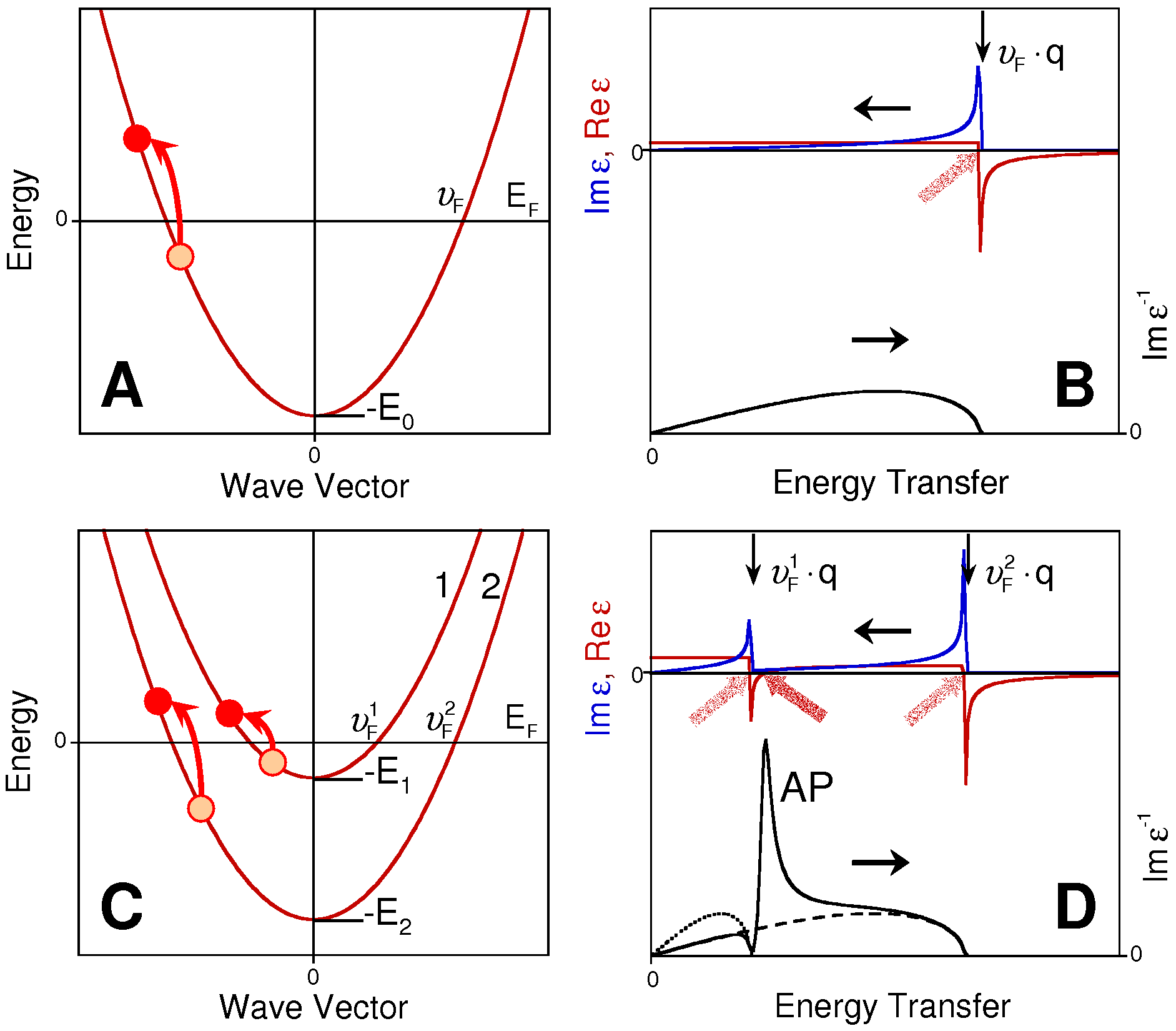
In order to understand the basic mechanism behind the ASP, let us compare the behavior of a conventional 2D electron gas with a parabolic dispersion (see Fig. 1 a) with an electron gas consisting of two components with different Fermi velocities (see Fig.1 c). The corresponding dielectric function for a given wavevector k (in the long wavelength limit) and the loss function are shown in the right panels of the same figure. For the 2D electron gas with only one component the low energy zero crossing of is not associated with a peak in the loss function and thus corresponds to the excitation of incoherent intra-band electron hole pairs. For a two-component electron gas there exist three zero crossings of at low energy. One of them is associated with a peak marked in the loss function . Since it lies just above the edge of single particle transitions within the band with the lower Fermi velocity, it corresponds to a collective mode screened by the electrons located in the other band. In the long wavelength limit, i.e. for , the energies of both peaks in disperse linearly with q. The peak in the loss function, being limited by such linearly dispersing peaks, exhibits also a linear dispersion and satisfies thus eq. 4. In the case of a Shockley surface state at a metal surface, the model still captures the essential physics, provided that one of the two components of the electron gas is associated to the 3D electron system and that the coexistence of 3D and 2D electron gases in the same volume is properly considered.
It is worth mentioning here that this scenario of interacting electron gases is not limited to the specific case just discussed. E.g., stacking of identical layers, separated by insulating spacers, considered theoretically in ref. [23] also leads to coupling between electron gases and to linearization of plasmon dispersion.
The plasmon dispersion can be measured experimentally by using (highly resolved) Electron Energy Loss Spectroscopy (HREELS). An instrument with simultaneous high energy and high momentum resolution is called ELS-LEED [50]. Electrons with energy impinge at an angle with respect to the surface normal. Electron can scatter elastically or inelastically. The energy spectrum of the electrons scattered at an angle from the surface normal can contain peaks at energy . The energy lost (or gained) corresponds to the creation (or annihilation) of a collective excitation of energy such that:
| (5) |
Note that is positive when the excitation is created and negative if it is destroyed in the scattering event. The conservation of momentum in direction parallel to the surface reads:
| (6) |
where is any reciprocal lattice vector of the surface unit cell. Since before and after scattering the electron is a free particle (the same relationship holding also for any free particle with non-vanishing mass in the non relativistic limit) the modulus of the parallel component of the wavevector is given by:
| (7) |
The modulus is given by a similar relationship. It is thus possible to obtain and , i.e. the dispersion relation of the collective excitation (or the energy and the momentum of the particle) created in the scattering event. Experiments performed for Ag on Si [13] and for [51] confirmed the prediction. At very long wavelengths, 2D plasmons have low energy. However they are unable to affect electron-phonon interaction and phonon dynamics close to the Fermi energy because of the square-root dispersion.
2.2 Sheet plasmons in 2D
2.2.1 Metallic layers
a)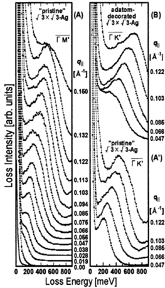 b)
b)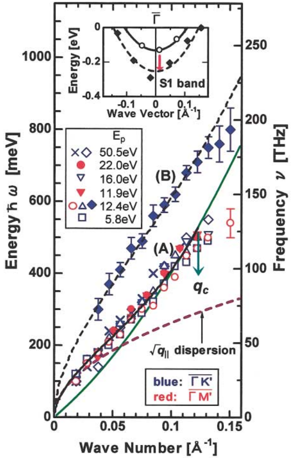
Here we discuss the prototype system Ag/Si(111) [13]. Similar results have been obtained for Dy/Si(111) [51]. The flat Ag/Si(111) system has been a prototype for the investigations of surface conductance on a low-doped Si substrate [52], in which metallic conductance has been shown to be associated with the formation of a R structure. Conductance can be changed by adding further Ag atoms. In fact, such -structure turned out to be a semi-metal [30], and metalliticy is attained only by adding surplus Ag atoms to this structure [52]. The most natural explanation for this self-doping phenomenon seems to be the formation of a lattice gas in the second layer, as also suggested by a HREELS study as a function of Ag concentration [53]. The investigations on stepped Si(557) yield however a somewhat different picture (see below).
In any case, 2D metallicity can be generated in this system. A direct proof is the existence of a plasmonic excitation whose energy goes to zero at long wavelengths, no further excitation being necessary to create this plasmon. The first test for such a purely 2D system has indeed been carried out in Ag/Si(111) at monolayer concentration [13]. The main results are shown in Fig. 2.
As seen in Fig. 2b), the dispersion can be well described by a 2D non-relativistic NFEG using the two terms given explictly in eq. 1. Within errors there was no angular dependence of the dispersion, but the slope of dispersion changes when further Ag was added to the (already self-doped) R30∘-Ag structure. From their fits the authors determined electron concentrations between 1.9 and cm-2 and an effective electron mass around . This result is in good agreement with data from angular-resolved photoemission (ARPES) for the same system [30]. From these numbers an effective electron transfer of about 1/3 of an electron per surplus Ag atom was deduced. For the present case, the screening by the substrate can thus be accurately described by an effective dielectric constant of the interface.
2.2.2 Plasmons in the 2D relativistic electron gas
Since its final discovery in 2004 [54] graphene has become one of the most studied materials in nanoscience. The coupling of light into flat and nanostructured graphene in the terahertz and far infrared frequency regime, using the plasmonic properties of graphene in order to form surface plasmon polaritons (SPP) has been a widely covered subject [55, 56, 57], and many potential applications have been suggested [58, 59, 60, 61]. We refer the reader to these excellent reviews and will not elaborate on these topics here, since although in this range of frequencies sub-wavelength phenomena (compared with optical and infrared wavelengths) can be observed, the typical wavelengths of several m do not allow to enter the nanoscale of 10 nm and below.
However, there is a unique property of 2D plasmons that have became obvious by studying 2D plasmons in graphene. Here we concentrate again on the low-energy plasmons. Other plasmons in graphene, in particular the standard plasmon excitations has already been reviewed before [15] and we refer the reader to this literature. At low (typically in the range of m-1), i.e. at plasmon frequencies in the terahertz range, a series of studies have exploited the fact that the plasmon frequencies of plasmon polaritons, i.e. the combined excitation of a plasmon in an external electromagnetic field, can be tuned by changing the carrier concentration in the graphene layer. This can most conveniently be done by using a gate voltage [62, 63]. Thus plasmon polaritons at a wavelength of a few hundred nanometers can be excited with light in the far to middle infrared range. This result is attractive because its relatively low damping: decay lengths reaching 1m allow indeed to foresee many perspectives potential applications such as tunable infrared lasers [64], plasmonic quasicrystals [58], ultrasensitive detection down to the single-molecule level [65], improved photovoltaics,[66], or nonlinear optics [67]. This tunability, however, is subject to certain physical limitations that we will describe further below.
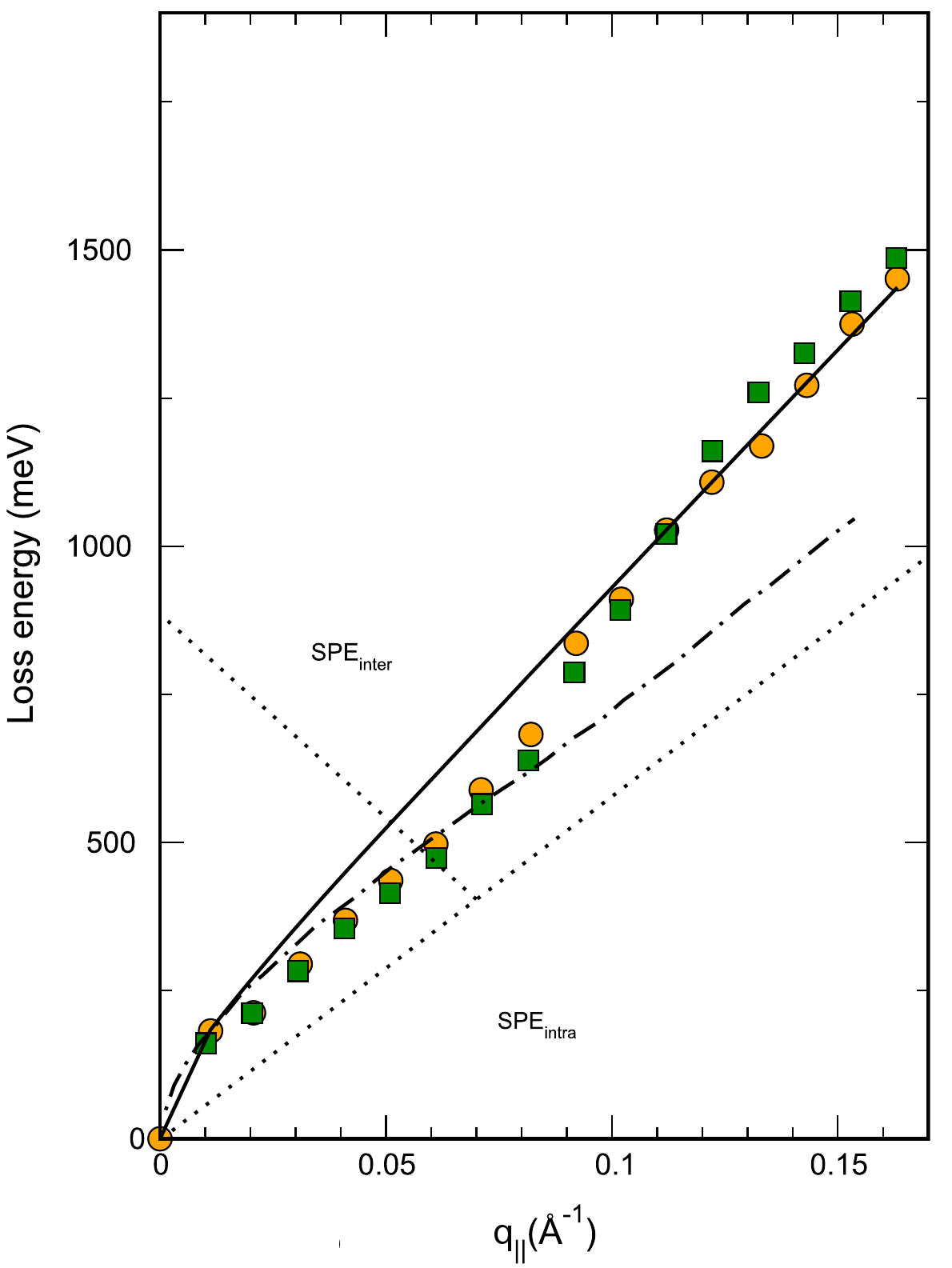
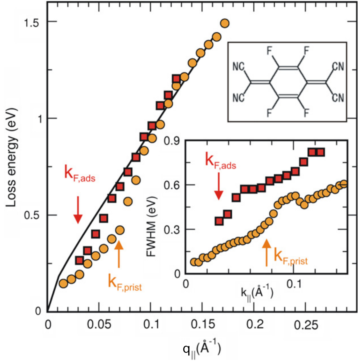
Surprisingly, this tunability seems to completely disappear, when is in the range of 1 nm-1. An example is shown for graphene on Si-terminated 6H-SiC(0001) in Fig. 3. The left part shows the plasmon dispersion, recorded with electron energy loss spectroscopy with simultaneous high momentum and high energy resolution [68]. These results agree well with those of ref. [69]. The first layer of graphene on SiC grows on a carbon buffer layer. It turns out to be n-doped with a doping concentration of cm-2, and the Fermi level under these conditions is about 400 meV above the Dirac point [68].
At very low the dispersion is compatible with a dispersion, as predicted by the first term of eq. 1. It clearly deviates from this function already at Å-1, similar to the Ag/Si(111) case discussed above. For Å-1, on the other hand, there is a linear slope of m/s, very close to the Fermi velocity in graphene on SiC [70]. Between these two regimes there is a characteristic cusp that was ascribed to resonant damping since the plasmon dispersion enters the continuum of single particle interband transitions.
Qualitatively, the experimental dispersion curve follows the theoretical curve developed for a 2D Fermi gas of relativistic electrons within the random phase approximation (RPA) [71]. The resonant damping has not been considered in theory. Nevertheless, there is still a cusp seen in theory (see Fig. 4), which is a characteristic property of the relativistic electron gas. It is much less pronounced than in experiment because of the neglect of damping in the theoretical calculation. Therefore, quantitative agreement between theory and experiment cannot be expected.
The main qualitative difference between the non-relativistic and the relativistic 2D electron gas comes from the second term in the expansion of plasmon dispersion, which becomes dominant for large . This term disperses linearly with a slope , as already outlined above (see eq.1). For the relativistic electron gas of graphene, this limit is reached for [71]. If this second term dominates, its slope, according to eq.1, does not depend on the embedding environment. Even more important, for the relativistic electron gas with a constant Fermi velocity this term is independent of the doping level. Thus the slope of the dispersion in this limit should be usable as a calibration standard. This prediction can easily be tested.
One test is shown in the right part of Fig. 3. Here the plasmon dispersion curves before and after covering the graphene layer with about one percent of a monolayer of 4F-TCNQ molecules at 300 K are compared. F4-TCNQ is known to reduce the carrier density of graphene and hence to shift downwards [72]. As expected, the dip shifts to lower values (to Å-1). This shift is also seen in the resonance of the FWHM. Since the added molecules act as scattering centers, the loss structure is further broadened. This reduction of the doping concentration to cm-2 also reduces both and correspondingly. Therefore, the transition to the linear part of the dispersion happens at smaller , as expected from the considerations mentioned above, and the linear range is extended. The average slope of the linear part, however, remains unchanged, in accordance with a constant Fermi velocity and eq. 1. A very similar behavior has been found for a quasi free standing graphene layer on SiC(0001), generated with a graphene buffer layer by intercalation with hydrogen, by gradual desorption of the hydrogen [73], which mainly shifts the Fermi level and thus the doping concentration.
A second example of this finding is shown by comparing these results with those obtained for graphene on Ir(111) [74, 75]. The graphene layer on Ir grows self-limiting as one layer by decomposition of hydrocarbons (ethylene) at temperatures around 1320 K, at a pressure of Pa. It is characterized by a Fermi level very close to the Dirac point [76, 77], i.e. a doping concentration of less than cm-2. Therefore, and in accordance with the results just presented, only a linear slope can be observed within the range resolvable with ELSLEED. This result is shown in Fig. 5 together with the results obtained after doping the layer by intercalation with half a monolayer of Na and in comparison with those from SiC. Here we concentrate first on the lower dispersion branch. When comparing the slopes of the quasi linear dispersion for graphene on Ir(111) with that on SiC(0001) (middle panel of Fig. 5), they are virtually identical. While the more effective shielding of the metallic surface compared to SiC should lower the slope of dispersion [70], this shielding is not static and leads to a more complicated interaction between the 2D electron gas of graphene and the 3D electron gas in the conduction bands of Ir, which may compensate the expected red shift. However, this effect has not been studied quantitatively in this system. Completely linear dispersion has also been found for graphene on Pt(111) [78, 15]. The slope, however, is about 15% smaller than in the examples just shown, possibly due to different interaction and shielding compared with the Ir(111) substrate.
Intercalation of graphene on Ir(111) by half a monolayer of Na has the effect of strong p-doping of graphene due a shift of the Fermi level of graphene by nearly 1 eV. As a consequence, linearity of plasmon dispersion is only seen over a reduced range upto 0.1 Å-1, whereas for higher values there is a tendency for levelling off. The slope measured in the linear range is about 10% larger compared to graphene on clean Ir(111). This is a remarkably small effect considering the change of doping level by about four orders of magnitude. On the other hand, both findings indicate that Na intercalation not only rigidly shifts the graphene bands, but Na interacts more strongly both with graphene and Ir causing the deviations measured. The increase in measured halfwidths of plasmon losses also point in this direction [75].

In view of eq. 1, these results are not expected, since the doping level considerably increases the first term of this equation, so that it should dominate over a larger range of . A clear dependence of the plasmon dispersion has indeed been seen on SiC(0001) by varying amounts of intercalated potassium [79]. In fact, due to the high doping level studied there, this first term of eq. 1 dominates most of those results, and there is semi-quantitative agreement with the predictions of eq. 1 with this assumption. At this point, we want to stress, however, that the findings of ref.[79] are not in contradiction to the results found on Ir and the others discussed above. On the contrary, they fully agree with the predictions of eq. 1. Since on a metal the screening is much more effective, the dielectric function is up to 2 orders of magnitude larger than for SiC, so that the first term of eq. 1 is smaller by the same factor on metals like Ir or Pt compared to SiC: the linear term in thus dominates already at small . Moreover the interaction with the shielding metal electrons leads to further linearization of the dispersion curves [23, 24], a mechanism not present on a semiconductor like SiC.
From these results we conclude that the tunability of the plasmon frequencies in the relativistic 2D electron gas is only possible if the term dominates the dispersion. The strong sensitivity of this term to the environment via its dielectric function not only influences the accessible frequencies, but also the range of tunablity. This range can easily be exceeded particularly on metals, where the term linear in is responsible for the insensitivity of plasmon dispersion to the doping level and to the environment. This robustness hasn’t been exploited yet, but is quite important for many potential applications.
2D plasmons were also shown to couple to other excitations, in particular to phonons and single electron excitations. The enhanced coupling of plasmons to single particle excitations is quite well known: similarly to the situation described above [68] due to opening of new decay channels, it causes resonantly enhanced damping. Similar phenomena have also been observed in photoemission, but here the linear dispersion of (ideally) non-interacting single quasi-electrons and -holes is modified close to the Dirac point by the interaction with the plasmon due to excitations of so-called plasmarons [80, 81]. F or the coupling between sheet plasmons and phonons a prominent example is the coupling in graphene to the surface optical phonon of the underlying SiC on the Si-terminated surface [82, 83]. The coupling of this phonon turned out to be remarkably robust. It cannot be quenched by intercalation and modifications of the intercalation. Instead, new coupled modes appear that are due to the coupling between the sheet plasmon with phonons of the intercalated material. Only for bilayer graphene coupling of the plasmon with the internal LO phonon was found to be detectable. These coupling may give a further handle to tailoring plasmonic properties.
Finally, we turn to the observation of multipole modes, which were identified for graphene on Ir(111) and on SiC(0001) [75]. As seen from Fig. 5, these modes follow closely the dispersion of the basic mode, but with a different slope depending on the substrate material. On the metal the ratio between slopes is roughly 2, while on SiC it is reduced to 1.4. The halfwidths of the multipole losses turned out to be essentially the same as for the basic mode. Both modes appear at the same so that it seems that both modes are excited by the same mechanism. It is indeed only a matter of probability which one dominates. The different ratios of slope found on the metal and on the semiconductor may, on the other hand, be due again to different efficiency of screening. These multipole modes in low-dimensional systems have not been explicitly considered by theory yet, even if this improvement is highly desirable in order to get deeper insight.
2.2.3 The acoustic surface plasmon (ASP) for Be(0001), Cu(111) and Au(111)
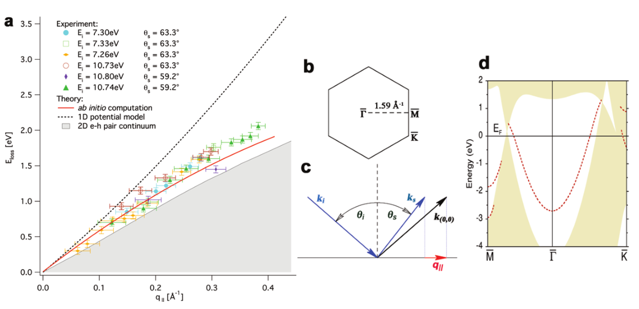
As mentioned in the Introduction, a new mechanism of linearization of plasmon dispersion comes into play when excitations of different electron gases can be coupled. An important example is the 2D electron gas of a Shockley surface state, which exists, e.g., on the close-packed surfaces of the noble metals (Ag(111), Au(111) and Cu(111)), but also on Be(0001). The 2D sheet plasmon will inevitably be screened by the underlying 3D electron gas of the metal. The ASP was first observed experimentally on Be(0001) with HREELS. Experimental data are shown in Fig. 6 along the direction for two different kinetic energies (7.26 and 10.74 eV) while keeping the scattering angle fixed (63.3∘ and 59.2 ∘) and changing the angle of incidence . The parallel momentum is obtained using eq. 6.
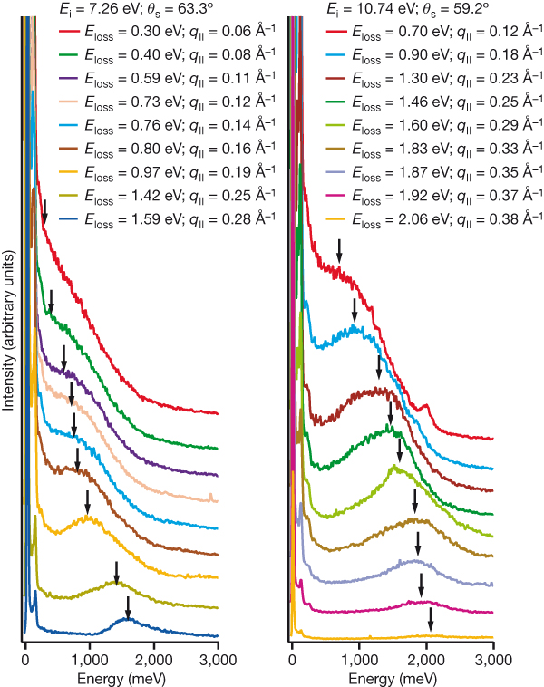
It is apparent that a relatively broad energy loss feature is present and that it shifts to higher energy with increasing parallel wavevector. The position of the loss feature for several scattering conditions is shown in Fig. 7. The slope of the dispersion curve turned out to be 5.5 eV (for comparison: 1 eV m/s), slightly lower than predicted by a simplified 1D model and in very good agreement with the prediction of a more accurate ab-initio model. Measurements along were performed by another group [17]. The slope (group velocity) came out to be slightly higher (6.4 ) than for the direction. Moreover along the high symmetry direction the ASP has a larger width than along due to the fact that the ASP dispersion is closer to the electron-hole pair continuum along [84].
The discovery of the ASP on Be(0001) triggered further measurements on other surfaces such as Cu(111) [18] and Au(111) [21], for which theory had already predicted its existence. For Au(111), actually two linearly dispersing losses were found [20] with group velocities of 3.95 and 8.1 , respectively. Only the latter loss was seen in ref. [21]. A selection of spectra for different scattering conditions and the dispersion curves are shown in Fig. 8. According to time dependent DFT calculations [20], however, only the first with the lower slope corresponds to the ASP, whereas the second higher energy branch was assigned to an interband transition between a band edge of the bulk and the Shockley surface state. A further contribution to this loss from a multipole ASP cannot be excluded.
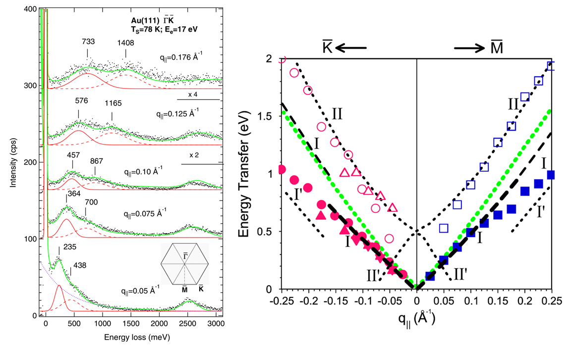
Interestingly, as seen from Fig. 8, the slope of the low energy branch corresponds to a value of 1 in eq. 4, i.e. to a loss running slightly below the edge of the electron - hole pair continuum. As demonstrated theoretically [20], this is a particular screening effect of the surface state excitation by the bulk electrons. For Au(111) the electrons in the Shockley surface state close to the Fermi level have velocities higher than the corresponding majority of bulk electrons, thus leading to a value of slightly lower than 1. The complication with two losses also appeared for the Cu(111) case, as a recent investigation with very high energy resolution showed, i.e. the loss feature assigned to the ASP by Pohl et al. [18] consists actually of two losses. The component with the lowest slope among them was then assigned to the ASP for Cu(111), suggesting a scenario similar to Au(111) [49]. Thanks to the higher energy resolution, the width of the ASP is now lower than estimated before: using the time-energy principle of indeterminacy, it is thus possible to estimate the lifetime and the propagation length of the ASP, a parameter relevant to assess the feasibility of ASP-based devices.
2.2.4 ASP for nanostructured and regularly stepped surfaces
After having shown that the ASP exists for most of the surfaces for which its existence had been predicted, a quite natural question arises: How robust is this excitation? Is it affected by surface nanostructuring? In order to address such issues, experiments for both ion bombarded Cu(111) and for stepped Au surfaces were performed. In the former case domes and pits of different size form upon ion bombardment, the morphology of which is determined by the interplay between thermal diffusion and removal of atoms by the incoming ions. In the latter case an ordered array of terraces separated by monoatomic steps is present. The ASP turns out to be a relatively robust excitation: it is not destroyed by surface nanostructuring both at RT and at 393 K, at least for moderate ion doses [19]. The linear best fit to the dispersion data yields a slope of . This value has to be compared with that found for the pristine surface (, [18]). As demonstrated by Theilmann et al. [85] the Shockley Surface state (SSS) shifts from -0.4 eV to about -0.3 eV when the roughness of the Cu(111) surface is increased. This causes a decrease of the Fermi velocity and thus a decrease of the slope of the plasmon dispersion, in qualitative agreement with experiment. For large enough ion doses and while sputtering at 393 K a non-dispersing loss was observed and tentatively assigned to a non-vertical inter-band transition from the bottom of the SSS to the Fermi level, the required momentum being provided by surface disorder [19].
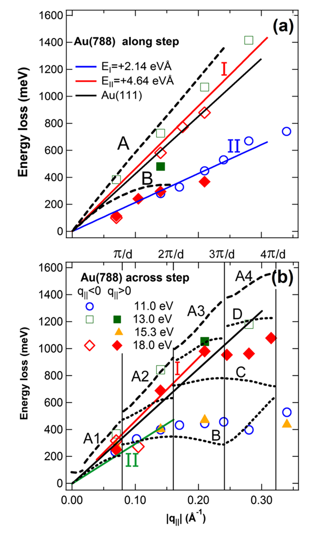
With decreasing wavelength, also plasmons become more and more susceptible to scattering at atomic defects. This effect has clearly been seen for plasmons scattered at substrate steps in graphene on SiC(0001) [87]. On a metallic surface, scattering at steps is expected to be smaller due to the less directed bonds, but as was demonstrated for the regularly stepped Au(788) surface, it leads to subband formation and partical localization of plasmons. The (788) surface consists of (111) terraces that are wide, separated by monatomic steps. The choice of this particular terrace size is motivated by the fact that the distance between steps exceeds the critical value (around for Au) beyond which the short-range interaction between steps becomes negligible, so that opening of an energy gap in the surface band structure can occur [88]. The choice of Au surfaces is motivated by their chemical inertness: the existence of the ASP is indeed closely related to the existence of a partly unoccupied Shockley surface state, which can in turn be destroyed by surface oxidation. The dispersion of the ASP for Au(788) was measured using an ELS-LEED setup [86].
The data are summarised in Fig. 9. Two losses with sound-like dispersion are present, denoted by I and II. The branch with the steeper slope originates from the ASP associated to the SSS of the (111) terraces, and has indeed a very similar slope as the ASP on flat Au(111). The branch with lower slope has no analogue on Au(111). Although fully ab initio calculations are not feasible because of the too large unit cell, it was possible with the help of theoretical calculations to assign all the features observed experimentally [86].
In particular we underline that:
-
(a)
Along the steps two ASP modes exist. They have different group velocities determined by the Fermi velocities of two partly occupied SSS sub-bands.
-
(b)
The anisotropy introduced by the steps on Au(788) does not automatically lead to plasmon localization normal to the terraces.
-
(c)
The QW1 and QW2 sub-bands are still able to generate propagating plasmonic modes across the steps at wavelengths longer than the terrace width. The slightly different slopes of the modes parallel and normal to the steps reflect the anisotropy of the system.
-
(d)
Across the steps, plasmon localization becomes visible when exceeds the reciprocal lattice vector of the periodic step array.
The interest for the effect of the presence of a regular array of steps on the ASP existence and dispersion is not purely academic: it has been suggested indeed that vicinal surfaces might provide naturally a diffraction grating of the nanometric size needed to couple the ASP with light [7]. Due to the large difference between the speed of light and the Fermi velocity in the Shockley Surface State (almost 3 orders of magnitude!), an (infrared) photon with an energy of 0.5 eV could excite on Be(0001) an ASP with a wavelength of 50 to 80 , provided that a diffraction grating allows to bridge the momentum gap. A hypothetical device converting effectively photons into ASP should therefore have a characteristic spacing of that order, i.e. about two/three orders of magnitudes smaller than a traditional optoelectronic system operating at the same frequency.
Although some theoretical estimates for nanoparticles predict a low efficiency for the conversion of photons into ASPs [89], no experiments have been reported yet. In Table 1 experimental and theoretical values obtained for the slope of the ASP dispersion are summarised.
| System | Fermi velocity () | Experimental slope | ||
| () | (non ab initio: [24] ) | |||
| Be(0001) | 0.41 | 5.5 [16] | 1.08 | |
| Cu(111) | 0.28 | 4.33 [18] | 1.13 | 1.053 |
| Cu(111) | 0.28 | 3.11 [49] | 0.81 | |
| Au(111) | 0.35 | 3.95 | 0.83 | 1.032 |
| Ag(111) | 0.11 | - | - | - |
| Ag(111) | - | 7 [90] |
Summarizing the ASP observations, is apparent that the interaction between two electron gases provides a mechanism of mutual screening that leads to linearization of the dispersion, particularly also for small . Therefore, it is not described by eq. 1, which at small predicts a -dependence.
The fact that can be , as observed for Au(111), so that the ASP runs below the electron hole pair continuum, does not directly lead to overdamping of the ASP, as often assumed. Possible reasons are small overlap between SSS and bulk states, but also phase mismatch of wave functions, expressed by the different Fermi velocities of bulk and surface state.
The reliable calculation of these phenomena is still a challenge for simulations, as seen by two conflicting predictions for the Ag(111) surface: according to Ref. [90] this system should exhibit a slope even higher than for Au(111), while the non ab initio theory predicts a slope even lower than on Cu(111), in agreement with a third, independent calculation [91]. No experiments have measured the ASP dispersion for Ag(111) yet, so that this controversy remains open. On the other hand, the experiments carried out so far for ASP by HREELS measurements demonstrate that ambituities due to the appearance of several losses can only be resolved by reliable quantitative theoretical descriptions.
3 Quasi-one dimensional plasmons
As already demonstrated above for the case of Au(788), the introduction of extended defects such as steps on highly symmetric surfaces reduces the symmetry of surface states so significantly that subbands are formed, as also visible by two separate subband-plasmons for the two occupied subbands in the ground state. These plasmons, however, propagate across the steps for long wavelengths and get only localized to single terraces for wavelengths of the order of the terrace width. Therefore, they cannot be considered to be quasi-one dimensional.
On the other hand, the experimental observation of a purely 1D dispersion of a plasmonic signal is clearly a necessary condition for quasi-1D behavior, but is it sufficient? In the ideal case, a Tomonaga-Luttinger liquid may appear, in which, due to spin and charge separation of the lowest excitations, the plasmon should appear as a holon with a linear dispersion [92, 93, 94]. While there is no final answer to this question yet, we will discuss in the following systems in which the requirement of 1D dispersion is cleary fulfilled: the formation of metallic chains of single atomic height on regularly stepped Si surfaces. Regular arrays of these chains are formed by self-organization, and the widths of the wires vary from single atomic chains to metallic strips that fill a whole (111) terrace, depending on the metal, but also on the step orientation. The main question is of course, how strongly the potential 1D properties of these wires are modified by their environment and the coupling to neighboring wires. As it turns out, there is again a wide variation in the strength of interaction, which still has to be understood.
A possible approach to 1D plasmonic properties start from a 2D quasi-free electron gas that is confined to a wire of finite width by an appropriate potential. Within this model, following ref. [95], the plasmon dispersion for a single isolated wire can be expressed as a function of the upper and lower boundary of the electron-hole continuum of excitations, as
| (8) |
with . V(q) is the Fourier transform of the confining potential, the local field correction factor due to electronic correlations, and the spin degeneracy (1 or 2). Already this model yields to lowest order a dispersion linearin , contrary to a 2D electron gas. As one sees from eq. 8, the dispersion depends not only on electron density (via ) and effective masses, but also explicitly on the form of the confining potential, and electronic correlations. For the coupling between wires, no such analytic expression can be given, but an approximate description of coupling, valid in the limit of small [96, 97, 98] exist and will be discussed below for Au wires on Si surfaces.
3.1 Arrays of quasi-1D wires with small coupling
From the few investigations of low-dimensional plasmons carried out on quasi-1D systems so far, Ag/Si(557) [43, 99, 100] and DySi2/Si(100)vic. [41] are those systems in which the properties of individual wires seem to be dominant, i.e. the coupling between wires is weak. Since the plasmonic properties of DySi2/Si(100)vic. resemble those in the Ag/Si(557) system in many aspects, we concentrate here on the latter system.
As mentioned above, the Ag/Si(111) system is a prototype system for the investigation of 2D plasmons, since carrier concentration in the Ag-modified Si surface state can be tuned by Ag surplus concentration. Similar properties have been found in the Ag/Si(557) system by investigations of the concentration dependent plasmonic properties. Although the doping mechanism on the flat and stepped surfaces need not be exactly the same, these studies allow to gain some surprising insights, not only into the doping mechanism, but also into general plasmonic properties in 1D [43, 99, 100]. A possible reason for the decoupling of wires on different (111)-oriented mini-terraces in this system may be the separation of these terraces by (112)-oriented minifacets, which contain 3 atomic double-steps.
The atomic Ag wires formed in this system at coverages below 0.3 ML turned out to be semi-conducting. Low energy plasmons do not exist below 0.3 ML, therefore. The formation of metallic wires is coupled to the appearance of -order on the (111)-oriented mini-terraces, which have a local coverage of 1 ML.
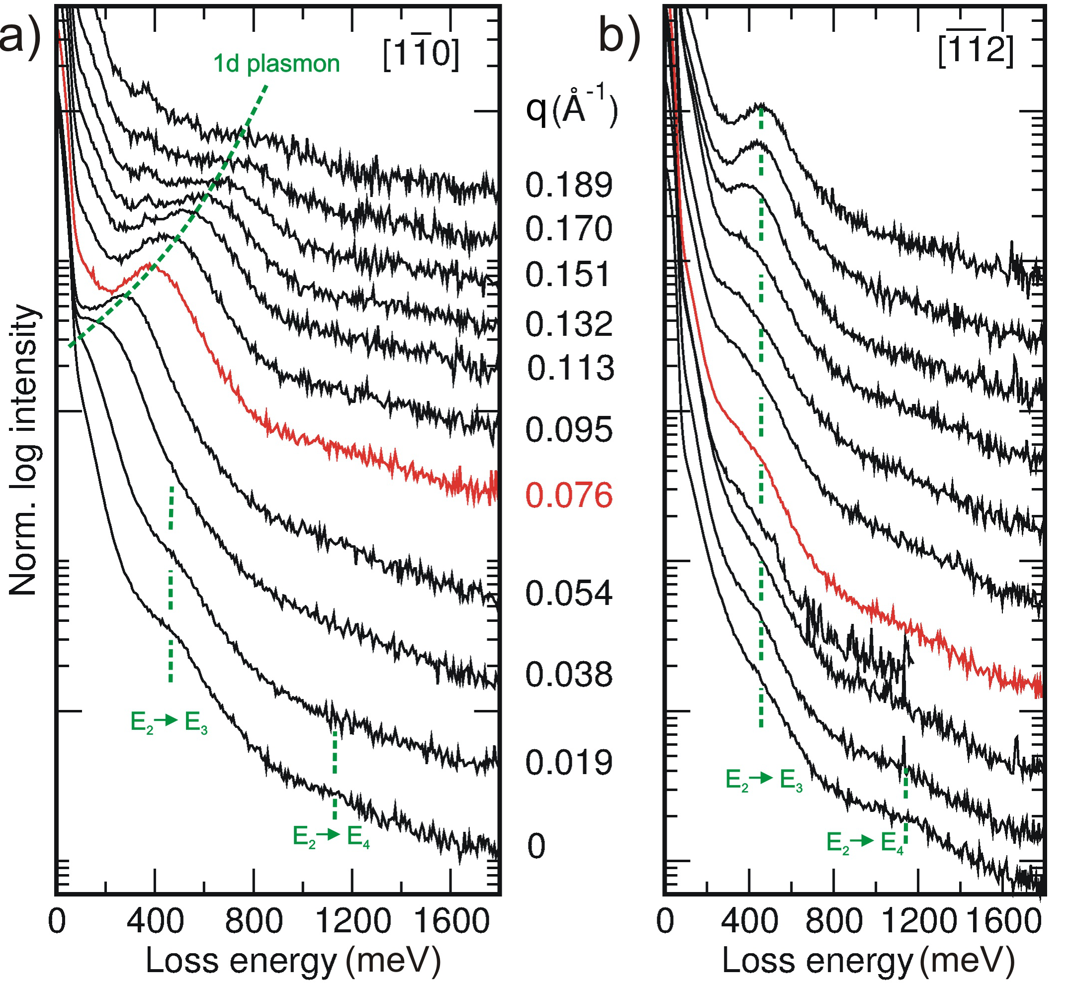
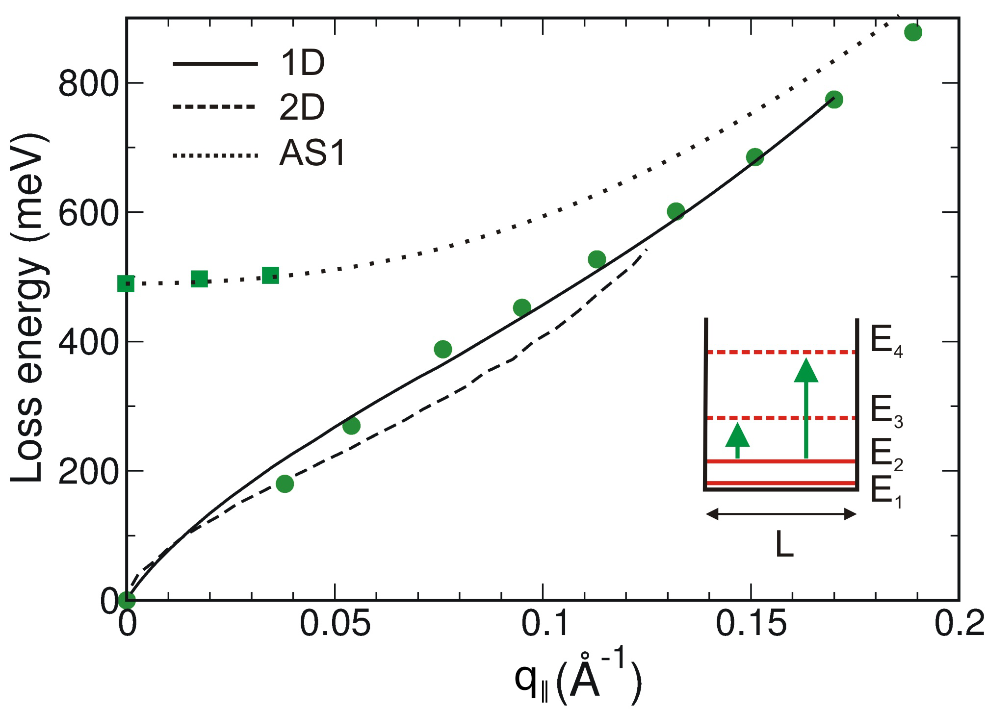
As seen in Fig. 10, a clear 1D dispersion was measured by EELS-LEED, which means that the triple steps between the (111)-terraces act as insulating separators between the conducting strips. Indeed, the measured dispersion for the lowest plasmon mode, shown in the right part of Fig. 11, agrees quantitatively with calculations [41], which assume a single strip of a 2D electron gas that is confined by parabolic barriers to a width of 3.6 nm. Not only the 1D dispersion is reproduced, but also the appearance of intersubband plasmons along the wires, which are expected to appear as coupled (and simultaneous) excitations of quantum well states and plasmons in these wires of finite width [44]. In the limit of long wavelengths they merge into the non-dispersing losses measured in the direction perpendicular to the wires (see Fig. 10b). They correspond to quantum well states formed normal to the wires. Their positions can be quantitatively fitted assuming a simple particle-in-a-box model with the measured wire width of 3.6 nm.
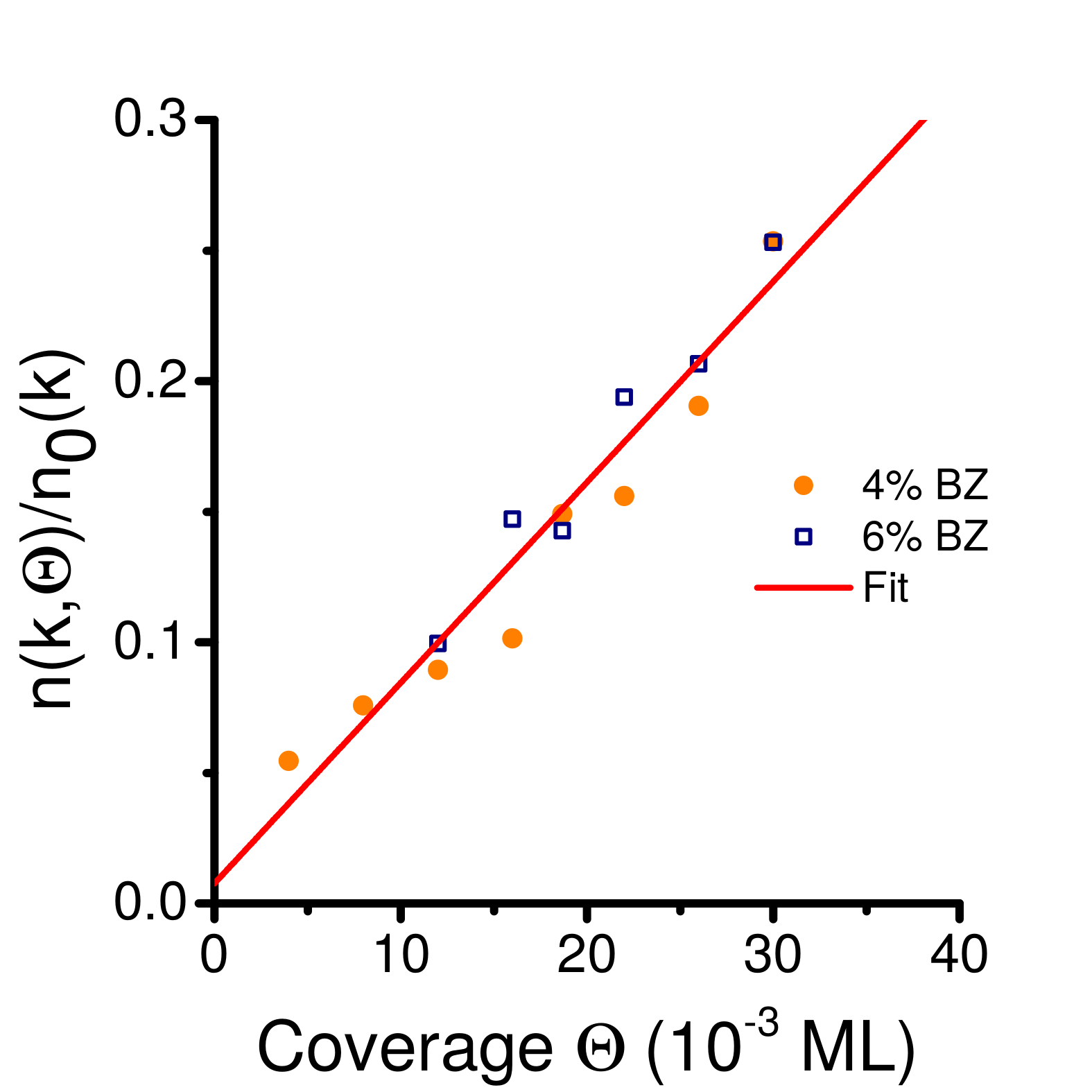
The metallic properties of the wires are not intrinsic, but are induced by extrinsic self-doping caused by Ag atoms adsorbed at the adjacent step edges, i.e. the bare Ag-wires with -order are semi-metallic. The doping atoms can be desorbed thermally without destroying the majority of Ag wires on the (111)-terraces, but can be made metallic again by the tiniest amounts of post-adsorbed Ag atoms. Thus this system allowed to determine precisely the dependence of plasmon excitation energy on doping concentration in the range between 0.003 and 0.03 of a monolayer. Assuming that all parameters except the electron density remain constant, and that each surplus Ag atom contributes the same amount of charge to the system at low concentrations, we found that , in agreement with theory (see also right part of Fig. 11). Remarkably, this dependence turns out to be universal, independent of dimension, and to be valid even for a Luttinger liquid. To our knowledge this is the first direct experimental verification of the dependence for plasmons in a quasi-1D system.
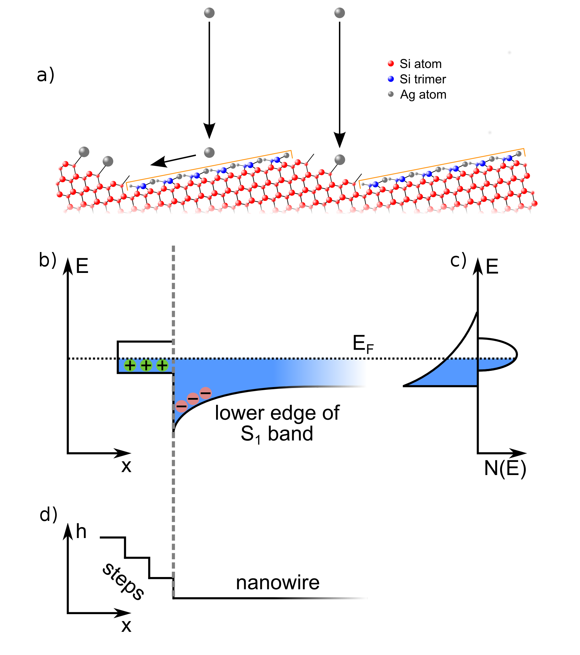
This lateral doping mechanism on the atomic scale is most likely caused by the different binding strength of Ag atoms on terraces and at step edges. It leads to preferential trapping of Ag surplus atoms at the step edges and results in lateral band bending, as sketched in Fig. 12. As a consequence, the effective wire width is reduced with increasing doping concentration, since the doping chains of atoms are partially charged. This charging also limits, depending on the chemical differences between terrace and step, the maximum doping concentration. Impurity atoms of different sorts can change this situation drastically, but this hasn’t been tested yet in any detail. These experiments also clearly ruled out the long debated doping process by a lattice gas in the second Ag layer, which turned out to be inactive with respect to formation of a low-energy plasmon.
The final proof for this model came from the fact that, similar to the Pb/Si(557) system (see below), also Ag/Si(557) modifies surface and step energies so that at high temperature (here 600∘C) the surface becomes unstable in the presence of a monolayer of Ag and tends to form larger (111) terraces and step bunches. Extended heating to 600∘C of the Ag covered surface roughly doubled the average terraces size. This allowed a unique proof of the extrinsic doping mechanism, since the line doping concentration remains essentially constant at saturation, but the overall concentration is reduced with increasing terrace size, since the mount of electrons donated by the dopant atoms is distributed over the larger (111) terraces [100].
3.2 Between 1D and 2D: Pb/Si(557)
The situation is much less clear in the Pb/Si(557) system, although at first glance it looks quite similar to Ag/Si(557). For a critical coverage of 1.31 ML and at low temperature (below 78 K) the system clearly has 1D properties in electrical conductance due to Fermi nesting and 1D band filling induced by facet formation. Facettiing locally transforms the surface into a (local) (223) orientation [31, 36] that causes the opening of a small 1D gap of 25 meV around the critical coverage. On the other hand, this high Pb concentration exhibits relatively strong electronic coupling between the terraces so that the general appearance of the band structure is 2D-like, although with 1D properties close to the Fermi energy. This leads to the following intriguing questions: are such 1D properties still visible in collective electronic excitations with excitation energies by far higher than the bandgap of 25 meV ? There may even be a transition between 1D and 2D behavior depending on the available decay processes into single particle excitations.
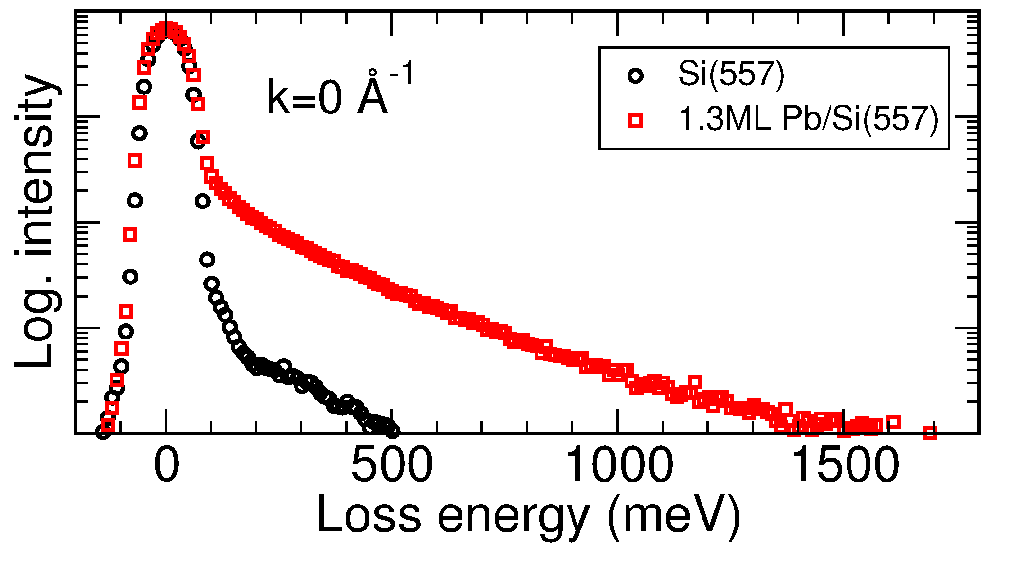
Metallicity of the layer at 1.31 ML Pb coverage can easily be identified even qualitatively by comparing the electron energy loss spectra for the clean and Pb covered Si(557) surface. Whereas for Si(557) only phonons can be created at small excitation energies, the continuum of low energy electronic excitations in a metallic system results in a broad structureless background with exponentially decaying intensity as a function of loss energy. This is a clear signature of metallicity for the monolayer Pb/Si(557) system.
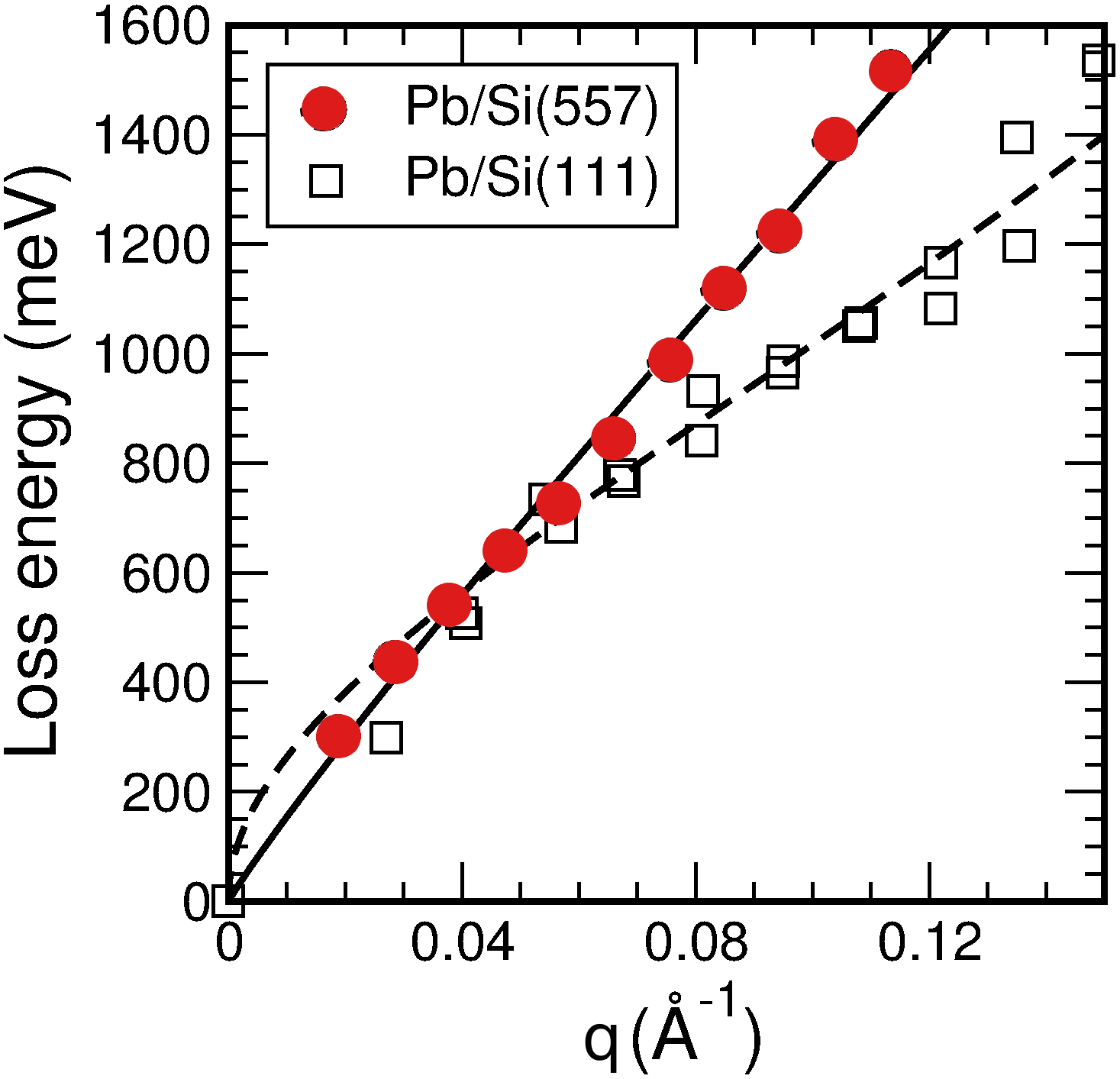
For the critical Pb concentration of 1.31 ML the HREELS spectra as a function of both parallel and perpendicular to the terraces were measured at room temperature and with He cooling (Fig. 13). No clear temperature dependence was found. While in the direction along the wires a clear dispersing loss peak was observed, no such loss was detected in perpendicular direction. In other words, plasmonic excitations have clearly a 1D dispersion at this Pb coverage. As seen from Fig. 14, the measured data points can be naturally extrapolated to zero momentum and zero energy. The dispersion can quantitatively be described by a model of a confined 2D electron gas with local field corrections and correlations [101, 44] using a single, four atoms wide metallic strip that is confined in a parabolic potential with the effective mass, , and the 1D electron density, , given in the caption of Fig.14. Further details can be found in ref.[42]. As seen also by the comparison with an analogous measurement for the isotropic Pb/Si(111) layer (see Fig. 14), there is a clear qualitative difference between a 1D and a 2D system (note that both dispersions must go through zero). Contrary to the Ag/Si(557) system [43], however, no indications for quantum well confinement were detected.
The missing temperature dependence of the 1D plasmonic dispersion can be taken as an indication that the physical mechanism for decoupling the plasmonic excitation on the various terraces cannot be related to Fermi nesting and opening of the 1D band gap alone. The absence of quantum well states means that the simple picture of a confining potential must be questioned. The key for this at first glance contradictory behavior may be hidden in the spin structure and the preferentially anti-ferromagnetic spin orientation on adjacent terraces, which leads to orthogonal electronic states. While there are no measurements, part of this spin correlation may still exist even at room temperature and reduce coupling. In the direction normal to the steps, the high resistance of steps [102], which at this Pb concentration turned out not to be covered by Pb [103], is already sufficient to prevent formation of plasmon waves in this direction. This situation, however, is modified by the gradual filling of step edges with Pb at higher Pb concentrations.
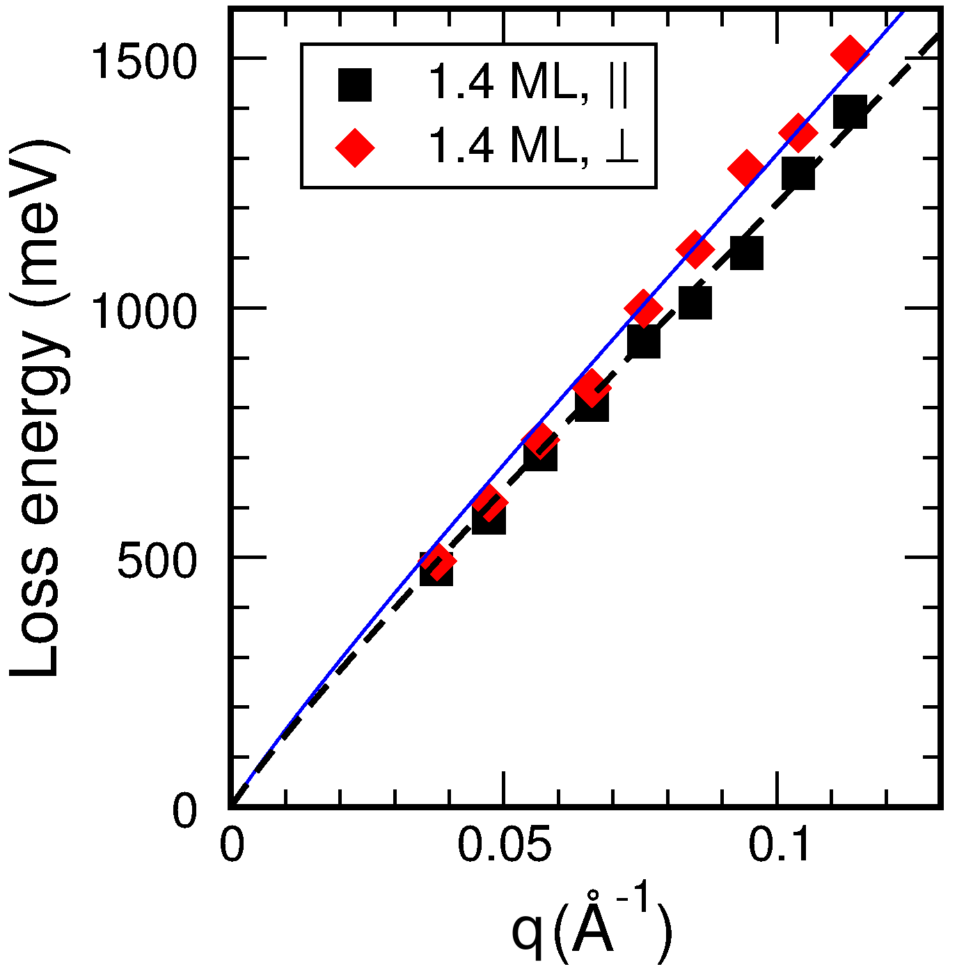
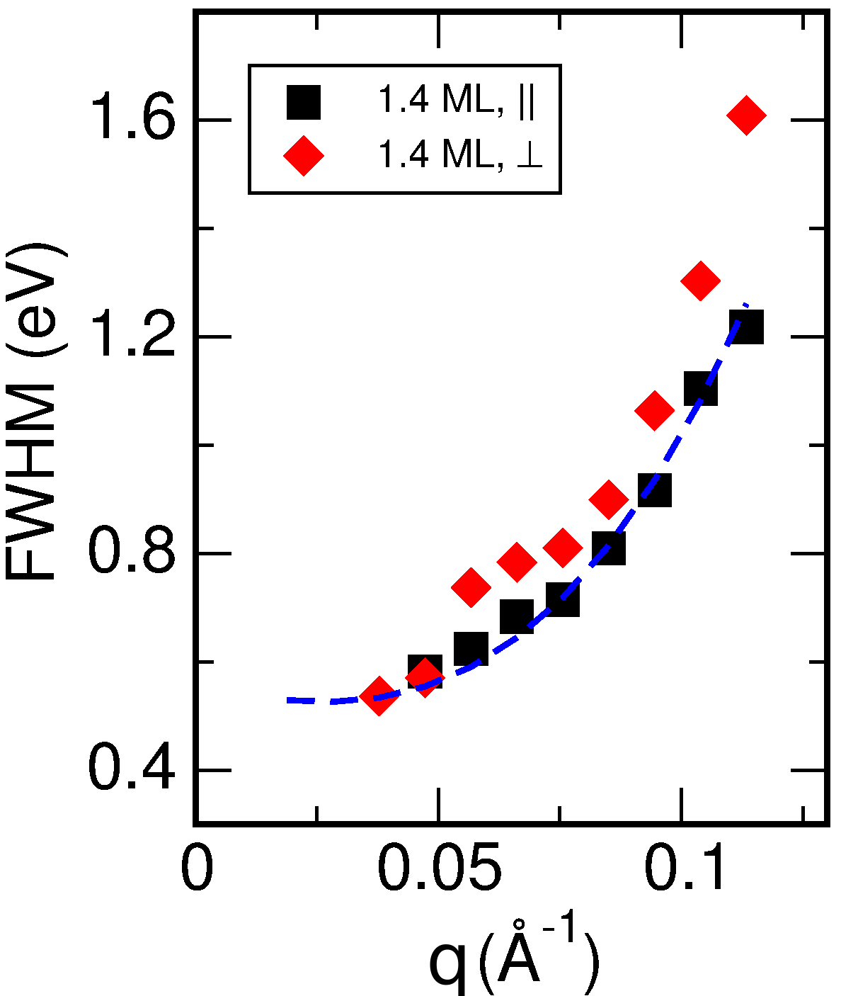
Interestingly, the quasi-linear dispersion remains when the steps are decorated by Pb, as shown now by increasing Pb coverage to 1.4 ML. At this Pb concentration about half of the Si step edges are decorated [104]. While these added chains increase coupling between different terraces, also the effective band gap is reduced [105]. Both changes in coupling parameters between terraces obviously now lead to the behavior documented in Fig. 15. While there was no detectable signal for long wavelengths, losses and their dispersion were found both parallel and perpendicular to the steps for wavelengths shorter than 15 nm, and with a quite small anisotropy of about 10%. This means that when changing the coupling between terraces, dispersing plasmonic excitations appear with wavelengths that exceed up to ten times the terrace width.
It should be noted that in both directions still a quasi-linear dispersion is detected, similar to the Au(788) system discussed above. Anisotropy seems to be sufficient for linearization of the plasmon dispersion. This finding may be obvious from eq. 8 for the direction parallel to the wires, but not in perpendicular direction. Contrary to the Au(788) surface, we find here that propagating and dispersing plasmons normal to the wire direction are found only at wavelengths considerably shorter than the undistorted periodicity of (223) facets. This lack of periodicity for distances larger than 20 nm of course also makes it impossible to form long wavelength plasmons here.
Thus there is a clear crossover behavior from 1D to 2D induced by a very small change of surface concentration of Pb. At this moment there is neither a clear understanding of the underlying physical mechanism for the crossover nor a quantitative theory for the plasmonic excitations in these anisotropic low-D systems.
Interestingly, the metal-insulator transition of In/Si(111), historically the first well investigated quasi-1D system [28], was seen not only in DC conductance, but could also be detected by the disappearance of the plasmonic loss [3, 40], in contrast to the Pb/Si(557) system.
These findings seem to be contradictory at first glance: the phase transitions in both systems are obviously of first order, though with opposite sign of temperature, the main difference lying in the structural changes involved. In Pb/Si(557) the Pb structure on each terrace essentially remains the same when going through the phase transition [106]. Just the average step distance is changed by only 3.5% [103], which turned out to be enough to destroy the nesting condition at the critical coverage of 1.31 ML, and to form a sequence of charge density waves with varying periodicity and decreasing band gap normal to the steps as a function of increasing Pb concentration [104]. Also the electronic changes in the bandstructure of this system associated with the metal-insulator transition seem to be small. The plasmon excitation seems to be quite insensitive to these small electronic changes. This scenario contrasts very much with the strong structural and electronic changes in the In/Si(111) system when going from the to the low-temperature phase [33, 107], which involves melting and disappearance of the whole CDW system.
3.3 Coupling in atomic wires: Si(hhk)-Au
Au chains on regularly stepped Si(111) surfaces, tilted at various angles towards the direction, provide the narrowest possible arrays of chains consisting either of one or two atoms, depending on the type of step. Here only double steps of Si separate the (111)-oriented terraces. Although purely 1D dispersion along the chain direction is found, the lateral extension of the charge distribution, determined both by the structural motif and the terrace width, turns out to explicitly influence the slope of the measured plasmon dispersion curves. In other words, the crossover into the second dimension is crucial for the quantitative interpretation of this quasi-1D phenomenon, but is not described completely by existing theories.
Depending on coverage and vicinality, the widths of the Au-chains and their interwire spacing can be tuned, while their electronic band structures are still very similar. 0.2 ML of Au on Si(557), e.g., result in growth of single atom Au-chains and a row of Si-adatoms on each mini-terrace with an interwire spacing of 19.2 Å [108, 3]. In contrast, Si(553) and Si(775)-Au host double Au chains in the center of the terrace [109, 34]. The interwire spacing is 14.8 Å for Si(553) and 21.3 Å for Si(775) [108, 110, 111]. For double Au chains, nominal coverages of 0.48 ML on Si(553) and of 0.32 ML on Si(775) result. Common to all these structures is a graphitic Si-honeycomb chain located at the step edges [108, 110, 111]. Each of these system is characterized by metallic bands that are well known from angular resolved photoemission (ARPES) measurements [108]. They only disperse along the chain direction , and have their minima at the zone boundary. Thus, also the (equilibrium) electron density available for plasmonic excitations is well known.
Here we compare the collective excitations in Si(553)-Au and Si(775)-Au, which have the same structural motif of the double gold chain. Furthermore, the Si(553)-Au system allows to vary coupling between wires, because it forms two phases. In the high coverage phase (HCW) at a Au coverage of 0.48 ML all terraces are covered with a double strand of Au, whereas in the low coverage phase at a coverage of 0.21 ML only every second terrace hosts the double gold chain [112, 45]. We will also make reference to the Si(557)-Au system with only a single gold chain.
Interestingly, the step structure also seems to have significant influence on the coupling between wires on different terraces. While the Au wires on Si(553) and Si(775) seem to be strongly coupled, as shown below, this coupling turned out to be weak for Au/Si(557) [95]. The plasmonic coupling between the wires in the ordered arrays, which is another aspect of dimensional crossover, is quantitatively modeled by existing mesoscopic theories [97, 98].
Contrary to the EELS spectra for Ag/Si(557) shown above, the spectra for all Au systems close to are structureless, apart from a small non dispersing feature that dies out quickly with increasing . Metallicity is demonstrated by the exponentially decaying background intensity as a function of loss energy, known as Drude tail [100], in agreement with findings from ARPES for the Si(553)-Au [108], STM [113], and theory [111]. However, this result is at variance with the ARPES data for the Si(775)-Au [108] for reasons still to be explored. In the direction along the wires, clear loss features are observed, which shift to higher loss energies with increasing scattering angles, i.e. with increasing . In the direction, however, and similar to Ag/Si(557), no dispersing mode is seen.
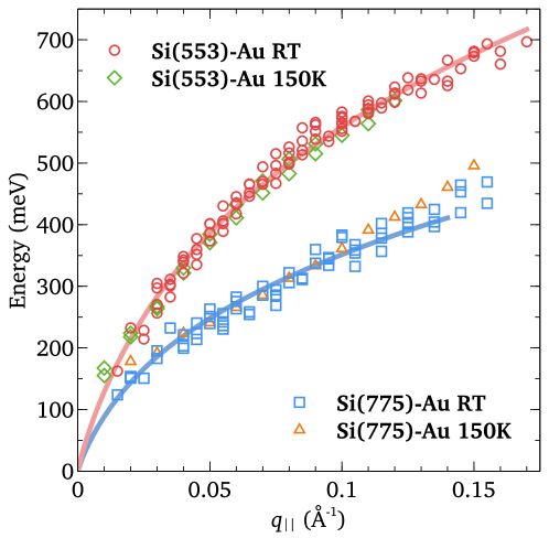
The dispersion curves along the wires, derived from the loss maxima, are shown for Si(775)-Au and for the HCW phase of Si(553)-Au in Fig. 16. From the ARPES data cited above, the ratio of electron densities and effective masses turns out to be virtually identical in the two systems for all surface bands. Therefore (see formula below), and in spite of two existing bands, only one plasmon loss is expected, in agreement with our findings. Thus for a true 1D system, no dependence on terrace width, d, is expected to first order. This is obviously not the case, since a 1/d dependence is found. Using existing theories for a nearly-free electron gas confined into quasi-1D wires [96, 97, 40, 114], a quantitative fit turned out to be possible with a modified model of coupled wires, sitting in a periodic array of square potentials at distance [97, 98]. At small , the dispersion is given by
| (9) |
where the first term of the product contains the electronic and structural properties of a single wire, the second the intrawire (first term under square root) and the interwire interaction. is the electron density per unit length, the elementary charge, the effective mass. is the dielectric function of Si as partially embedding medium. are modified Bessel functions of zeroth order and second kind, is the momentum normal to the wires. If (the effective wire width) is set equal to (a constant for normalization), eq. 9 corresponds to the original formula given in refs. [97, 98], which, however, turns out not to describe our findings. The ratio accounts both for differences in structural motifs and effective wire widths of a single wire, and is the only free parameter in eq. 9. In the array of square potentials the first term under the second square root accounts for the self-interaction of a single wire, whereas the second term describes the interaction between different wires at multiple distances of .
A further test to the sensitivity of the dispersion to the structural motif was carried out by fitting the published data of ref. [3] for Si(557)-Au to eq. 9. The Si(775) and Si(557) surfaces have almost the same terrace widths (21.2 vs. 19.8 Å, respectively). For the best fit the first term of eq. 9 has to be a factor of 1.6 larger for Si(557)-Au than for Si(775)-Au. Taking the differences in and the -dependence from above for the two systems, the effective width , as suggested in eq. 9, is reduced by roughly a factor of 2 for Si(557)-Au compared to Si(775)-Au. These results demonstrate that not only the periodicity, given by the wire distances , has a direct influence on the dispersion, but also the internal 2D distribution of the (excited) electron density within each wire. This result for Au/Si(557) is very much in agreement with the findings of ref. [95]. Subband excitations, as in the Si(557)-Ag system, can be ruled out here as possible source for the observed differences, since for these narrow structures and the given kF only the lowest subband of a quantum well is occupied. These results demonstrate that even in case of purely 1D plasmonic dispersion, there is a crossover to 2D, and both the width of a wire on the atomic scale and the internal electronic distribution within the very wire enter directly the slope of plasmonic dispersion. More details, e.g. about the choice of , can be found in ref. [45].
As it turns out, the LCW phase of Si(553)-Au can be described by the same formalism of eq. 9 [115]. In fact, according to the analysis of Song et al. [112], the Au covered terraces are supposed to have the same terrace width as in the HCW phase, whereas the empty terrace acts as separator between the Au wires.
This same effective wire width, however, does not reproduce the measured dispersion for the LCW phase, if we only assume reduced coupling between wires due to their increased interwire distance from 14.8 Å to 32.7 Å. By actually fitting the data with as a free parameter we obtain an effective wire width of 8.8 Å, compared to 7.5 Å for the HCW phase. This effective spreading of the plasmon excitation on the terrace is in fact quite plausible. In the LCW phase terraces not covered by gold are under tension [112] with the consequence of atomically rough edges. This gives the plasmon mode the possibility to spill out more into the uncovered neighboring terrace by approximately Å. Assuming the same proportionality factor between terrace width and effective wire width as for the HCW phase [45], a corrected value of 8.5 Å is obtained that is very close to the value obtained here. Therefore, this result fits into the general picture for the stepped Au covered Si surfaces that the electron density spills out as far as possible limited by the structure of the step edges, and expresses the crossover of two-dimensional properties on the one-dimensional plasmon dispersion. The effect of spillout of electrons in the LCW phase compared to HCW may be also taken as indication of softening of the confining potential. A softer potential than the square would in fact have a qualitatively similar effect at constant effective wire width.
Summing up this section, we demonstrated that the Si(hhk)-Au systems offer the unique possibility to study both the spreading of the chain-induced electron density on the mini-terraces and the influence of wire coupling in plasmonic excitations of quasi-one dimensional arrays of gold chains. As it turns out, there is an intriguing interplay between geometric terrace width and structural motiv that influences the effective wire width, as obvious from a comparison of, e.g., Si(775)-Au and Si(557)-Au. Coupling between wires, on the other hand varies both with terrace size and with the step structure. It is mainly the large average separation between terraces in the Si(557)-Ag system that makes them appear as essentially isolated wires. Weak coupling across Si(557) steps, which was found to be much weaker for Si(557)-Au than for Si(775)-Au, acts in the same direction.
4 Measured peak width of plasmon losses
So far, we have used only the information of peak positions, but we did not discuss the line widths of the plasmon losses. These loss peaks turned out to be fairly broad and not limited by the energetic resolution of the measurements. We discuss this problem using the recent example of Au/Si(553).
From a quick look at the measured width of the loss peaks, as shown in Fig. 17 for both Au phases on Si(553), particularly in the limit of , it is already obvious that these widths cannot be attributed to a lifetime, since in this limit the plasmonic excitation energies also go to zero. Consequently, the life times have to go to infinity. Taking the measured width as lifetime would mean that the plasmonic excitation is highly overdamped and plasmonic excitations would not exist. This is in sharp contrast to plasmons (at 125 meV) in comparable systems, where mean free paths exceeding 200 nm were observed [116]. Therefore, the FWHM at must be the convolution of instrumental resolution in reciprocal space and in energy of the spectrometer, possibly also with a contribution caused by the short interaction time of the electron scattering process. The energy resolution of the instrument, however, cannot be the main source of the measured half widths – it accounts to only up to 10% of the measured FWHM. Geometrical imperfections, as seen by the finite width in for the elastic peak, is another source, since it will cause corresponding averaging over the dispersion and thus energetic broadening. From systematic studies of LEED profile analysis it can also be safely ruled out here as a main source of broadening. The finite k-space resolution of Å-1, however, can be the main source of broadening, as seen by a comparison with the slope of dispersion of the HCW phase from Fig. 16. Since this slope is generally lower by about 30% for the LCW phase compared with the HCW phase, the broading in the limit of is correspondingly reduced, as indeed seen in Fig. 17. Therefore, the short interaction time of the inelastically scattering electrons as the possible reason for broadening seems to play a minor role. It may, however, not be negligible in the present case, since only near-field multipole scattering can be effective here – dipole scattering cannot transfer the momentum necessary for excitation – the scattering process being closer to impact scattering [117].
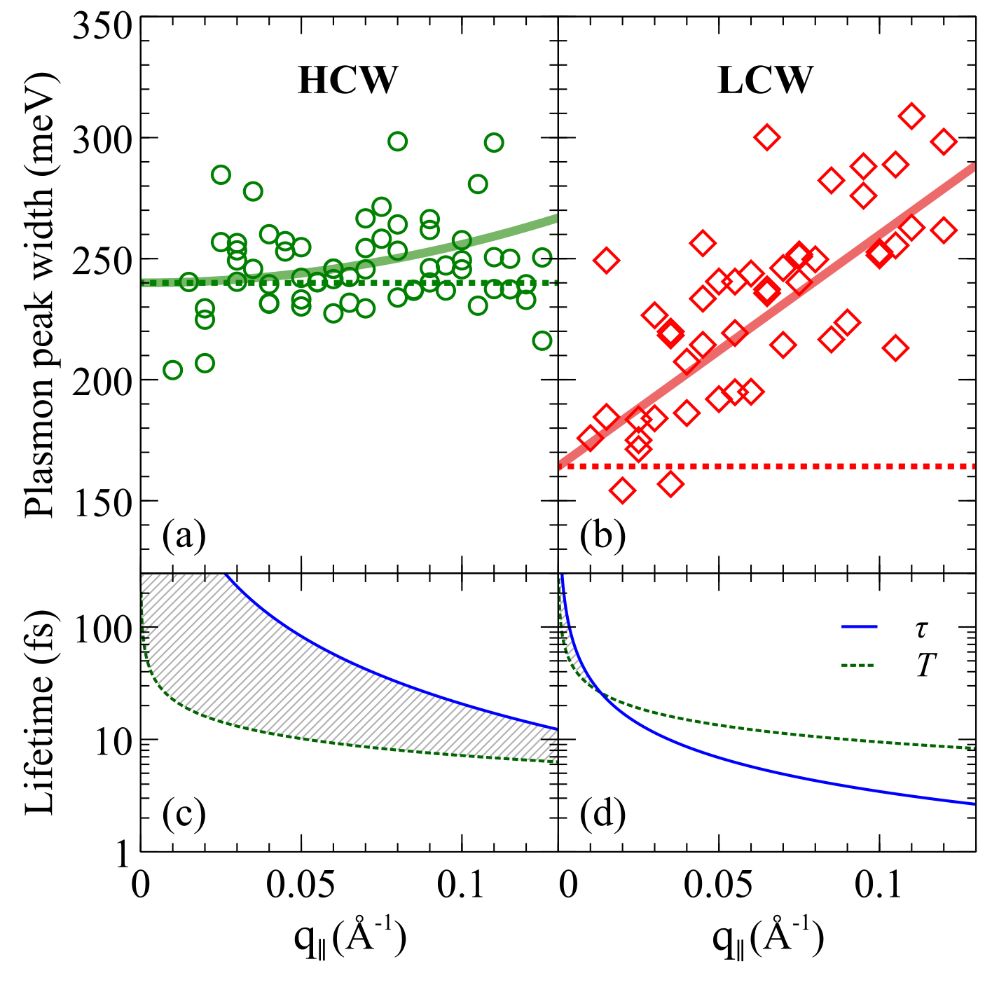
Starting from the FWHM at as an “instrumental” baseline, there is a tendency for a slight increase of FWHM by about 30 meV at Å for the HCW phase. This increase is much higher for the LCW phase and amounts to about 120 meV for the same range of . Two interpretations seem to be possible: broadening due to reduced lifetime with increasing energy of excitation, or inhomogeneous broadening caused by the existence of two plasmons.
For the HCW phase lifetime broadening alone seems to be a possible explanation for the observed increase in FWHM as a function of , depicted in figure 17(c). Using the procedures as just described, we approximated the increase of the peak widths by polynomial functions of second order (solid curves), subtracted the offset (dotted lines), and estimated the lifetime with Heisenberg’s uncertainty principle of , which yields the blue curve in the lower left part (c) of figure 17. This curve represents still a lower limit, since no broadening due to slight energetic differences in the two plasmon modes, especially at higher , was assumed to exist also here. In any case, it is compatible with other data [116].
For the LCW phase, on the other hand, lifetime broadening as the main source for the increase in FWHM can be ruled out right away. Assuming that we can simply subtract the halfwidths of the baseline from those measured, the determined “lifetime” as a function of quickly falls below the time necessary for a single plasmon oscillation, as shown in the lower right part (d) of figure 17. Of course, this overdamped situation is unphysical. Therefore, it seems to be more realistic that a large part of the broadening seen is due to the existence of two plasmons.
From the large linewidths of the plasmonic losses observed for both phases and their weak dependence on we conclude that the main contribution is not due to short life times, but even with the high momentum resolution of the present instrument is still mainly caused by the finite instrumental q-resolution, i.e there is still a need for further experimental improvement. While the two plasmons originating from the two Au-induced electronic surface bands cannot be resolved in both HCW and LCW phases, their larger difference in excitation energy in the LCW phase leads to an additional contribution to the measured halfwidths.
5 Conclusions
Considerable knowledge has been gathered on the dispersion of 2D sheet plasmons over the last 20 years. Plasmon dispersion in these systems - a few characteristic examples have been shown above - can surprisingly well be described by a nearly-free electron gas, even with the modifications of massless fermions in a relativistic electron gas. The inclusion of correlation effects beyond RPA seems to have mainly a quantitative effect on the general slope of dispersion. At long wavelengths, the dependence on electron density of plasmons in a non-relativistic electron gas, on the other hand, seems to follow the dependence in all dimensions. Only in the relativistic case it is reduced to .
Furthermore, two main possibilities for linearization of plasmon dispersion have been identified that are quite important for potential signal transmission via plasmonic coupling. The first one is due to the general form of plasmon dispersion (see eq. 1), if the second term of this equation dominates. This condition depends on , and it can be easily achieved at low electron concentrations and large . In the special case of a relativistic electron gas like in graphene, it leads to the observed insensitivity of plasmon dispersion on the doping level at large . In other words, tunability of plasmons in graphene by changes of the doping level only exists at long wavelengths (terahertz to far infrared range). The short wavelengths can still be used, but the strategy must be the selection of certain wavelengths, which are then quite robust against distortion. Particularly on metal surfaces, this range is even more limited due to the large value of the real part of the dielectric function of metals at terahertz frequencies.
Linearization of plasmon dispersion already in the long wavelength limit can be achieved by coupling of a 2D electron gas to other 2D or 3D electron gases, leading to the acoustic surface plasmon (ASP). This property has been demonstrated for the Shockley surface states on Be(0001) and on the (111) surfaces of noble metals, but this concept is fairly general. E.g. it might also be applicable for stacks of 2D metallic sheets separated by insulating material, or for stacks of graphene sheets, thereby combining linear dispersion with tunability.
In the anisotropic 2D case, which as a limit includes the quasi-1D wires, the situation less clear. While it is obvious that restriction of an electron gas to 1D leads to linearization of the plasmon dispersion already to lowest order in , there is an explicit dependence of dispersion on the form of the confining potential. Furthermore, the crossover into the second dimension by explicit consideration of the wire width and the role of coupling of plasmonic excitations with the environment is a general problem the description of which is still imcomplete. Also the role of correlations exceeding NFEG properties is still an open question. This sensitivity to the embedding environment, on the other hand, opens many still largely unexplored possibilities for tuning and manipulation both on the experimental and the theoretical side.
The present experimental setups, mainly electron loss spectroscopy (HREELS, EELS-LEED) still only allow limited studies of dynamics of 2D and 1D plasmons. The main limit is k-space resolution. It is obvious that there is sensitivity to atomic-size defects such as steps, which increases as a function of [87], i.e. there is high sensitivity to the quality of long-range order and its imperfection on the atomic scale.
The questions related to electronic effects in plasmon dynamics, on the other hand, is an
urgent problem that has been touched qualitatively at best, as our examples show. Since the low-D plasmons are
more strongly damped than, e.g., surface plasmons due to the conductive properties of the metallic sheets and wires,
but also of their environment, it is clear that solving these questions will be a key issue for any
application of these plasmons.
Acknowledgements
It is a pleasure to acknowledge the experimental contributions of the groups in Hannover and in Genova to several parts of this work,
in particular by T. Block, U. Krieg, T. Lichtenstein. We also strongly benefitted from collaborations and discussions with
the theory group at DIPC, San Sebastian, Spain, in particular by the collaboration with V.M. Silkin.
Financial support to this work by the Deutsche Forschungsgemeinschaft
mainly through FOR1700 and project Pf238/28 is gratefully acknowledged.
References
- [1] D. Pines, D. Bohm, Phys. Rev. 85, 338 (1952). DOI 10.1103/PhysRev.85.338
- [2] D. Pines, Rev. Mod. Phys. 28, 184 (1956). DOI 10.1103/RevModPhys.28.184
- [3] T. Nagao, S. Yaginuma, T. Inaoka, T. Sakurai, Phys. Rev. Lett. 97(11), 116802 (2006). DOI 10.1103/PhysRevLett.97.116802
- [4] R.H. Ritchie, Phys. Rev 106, 874 (1957). DOI 10.1103/PhysRev.106.874
- [5] H. Raether, Surface Plasmons on Smooth and Rough Surfaces and on Gratings, Springer Tracts in Modern Physics, vol. 111 (Springer, Heidelberg, 1988)
- [6] A. Liebsch, Electronic excitations at metal surfaces (Plenum Press, New York, 1997)
- [7] J.M. Pitarke, V.M. Silkin, E.V. Chulkov, P.M. Echenique, Rep. Prog. Phys. 70, 1 (2007)
- [8] W. Barnes, A. Dereux, T.W. Ebbesen, Nature 424, 824 (2003)
- [9] M. Jahn, S. Patze, I.J. Hidi, R. Knipper, A.I. Radu, A. Muhlig, S. Yuksel, V. Peksa, K. Weber, T. Mayerhofer, D. Cialla-May, J. Popp, Analyst 141, 756 (2016). DOI 10.1039/C5AN02057C. URL http://dx.doi.org/10.1039/C5AN02057C
- [10] S. Kawata (ed.), Near field optics and surface plasmon polaritons, Topcis in applied physics, vol. 81 (Springer, Heidelberg, 2001)
- [11] J. Grzelczak, M.and Pérez-Juste, P. Mulvaney, L.M. Liz-Marzán, Chem. Soc. Rev. 37, 1783 (2008). DOI 10.1039/B711490G
- [12] N.J. Halas, S. Lal, W. Chang, S. Link, P. Nordlander, Chem. Rev. 111, 3913?3961 (2011). DOI 10.1021/cr200061k
- [13] T. Nagao, T. Hildebrandt, M. Henzler, S. Hasegawa, Phys. Rev. Lett. 86, 5747 (2001)
- [14] E.P. Rugeramigabo, T. Nagao, H. Pfnuer, PHYSICAL REVIEW B 78(15) (2008). DOI 10.1103/PhysRevB.78.155402
- [15] A. Politano, G. Chiarello, Nanoscale 6, 10927 (2014). DOI 10.1039/c4nr03143a
- [16] B. Diaconescu, K. Pohl, L. Vattuone, L. Savio, P. Hofmann, V.M. Silkin, J.M. Pitarke, E.V. Chulkov, P.M. Echenique, D. Farias, M. Rocca, Nature 448, 57 (2007). DOI 10.1038/nature05975
- [17] M. Jahn, M. Muller, M. Endlich, N. Neel, J. Kröger, V. Chis, B. Hellsing, Phys. Rev. B 86, 085453 (2012)
- [18] K. Pohl, B. Diaconescu, G. Vercelli, L. Vattuone, V.M. Silkin, E.V. Chulkov, P.M. Echenique, M. Rocca, Europhys. Lett. 90, 57006 (2010)
- [19] L. Vattuone, G. Vercelli, M. Smerieri, L. Savio, M. Rocca, Plasmonics 7(2), 323 (2012). DOI 10.1007/s11468-011-9310-8
- [20] L. Vattuone, M. Smerieri, T. Langer, C. Tegenkamp, H. Pfnür, V. Silkin, E.V. Chulkov, P.M. Echenique, M. Rocca, Phys. Rev. Lett. 110, 127405 (2013)
- [21] S. Park, R. Palmer, Phys. Rev. Lett. 105, 016801 (2010)
- [22] F. Stern, Phys. Rev. Lett. 18, 546 (1967)
- [23] A. Bill, H. Morawitz, V.Z. Kresin, Phys. Rev. B 68, 144519 (2003)
- [24] V.M. Silkin, J.M. Pitarke, E.V. Chulkov, P.M. Echenique, Phys. Rev. B 72, 115435 (2005)
- [25] V.M. Silkin, A. Garcia-Lekue, J.M. Pitarke, E.V. Chulkov, E. Zaremba, P.M. Echenique, Europhys. Lett. 66, 260 (2004)
- [26] G. Güner, Density Waves in Solids (Addison Wesley, 1994)
- [27] P. Snijders, H. H.H. Weitering, Rev. Mod. Phys 82, 307 (2010). DOI 10.1103/RevModPhys.82.307
- [28] H.W. Yeom, S. Takeda, E. Rotenberg, I. Matsuda, K. Horikoshi, J. Schaefer, C.M. Lee, S.D. Kevan, T. Ohta, T. Nagao, S. Hasegawa, Phys. Rev. Lett. 82, 4898 (1999). DOI 10.1103/PhysRevLett.82.4898
- [29] J.N. Crain, A. Kirakosian, K.N. Altmann, C. Bromberger, S.C. Erwin, J.L. McChesney, J.L. Lin, F.J. Himpsel, Phys. Rev. Lett. 90, 176805 (2003). DOI 10.1103/PhysRevLett.90.176805
- [30] J.N. Crain, M.C. Gallagher, J.L. McChesney, M. Bissen, F.J. Himpsel, Phys. Rev. B 72, 045312 (2005)
- [31] C. Tegenkamp, Z. Kallassy, H. Pfnür, H.L. Günter, V. Zielasek, M. Henzler, Phys. Rev. Lett. 95, 176804 (2005). DOI 10.1103/PhysRevLett.95.176804
- [32] C. Blumenstein, J. Schäfer, S. Mietke, S. Meyer, A. Dollinger, M. Lochner, X. Cui, L. Patthey, R. Matzdorf, R. Claessen, Nature Phys. 7, 776 (2011). DOI 10.1038/nphys2051
- [33] S. Wippermann, W.G. Schmidt, Phys. Rev. Lett. 105, 126102 (2010). DOI 10.1103/PhysRevLett.105.126102
- [34] M. Krawiec, Phys. Rev. B 81(11) (2010). DOI 10.1103/PhysRevB.81.115436
- [35] T. Tanikawa, I. Matsuda, T. Kanagawa, S. Hasegawa, Phys. Rev. Lett. 93, 016801 (2004). DOI 10.1103/PhysRevLett.93.016801
- [36] C. Tegenkamp, T. Ohta, J.L. McChesney, H. Dil, E. Rotenberg, H. Pfnür, K. Horn, Phys. Rev. Lett. 100, 076802 (2008). DOI 10.1103/PhysRevLett.100.076802
- [37] C. Tegenkamp, D. Lükermann, H. Pfnür, B. Slomski, G. Landolt, J.H. Dil, Phys. Rev. Lett. 109, 266401 (2012). DOI 10.1103/PhysRevLett.109.266401
- [38] C. Brand, H. Pfnür, G. Landolt, S. Muff, J.H. Dil, T. Das, C. Tegenkamp, Nat. Commun. 6, 8118 (2015). DOI 10.1038/NCOMMS9118
- [39] T. Giamarchi, Quantum Physics in One Dimension (Clarendon Press, Oxford, 2003)
- [40] T. Nagao, S. Yaginuma, T. Inaoka, T. Sakurai, D. Jeon, J. Phys. Soc. Japan 76(11), 114714 (2007). DOI 10.1143/JPSJ.76.114714
- [41] E.P. Rugeramigabo, C. Tegenkamp, H. Pfnür, T. Inaoka, T. Nagao, Phys. Rev. B 81, 165407 (2010)
- [42] T. Block, C. Tegenkamp, J. Baringhaus, H. Pfnür, T. Inaoka, Phys. Rev. B 84(20), 205402 (2011). DOI 10.1103/PhysRevB.84.205402
- [43] U. Krieg, C. Brand, C. Tegenkamp, H. Pfnür, J. Phys. Condens. Matter 25(1), 014013 (2013). DOI 10.1088/0953-8984/25/1/014013
- [44] T. Inaoka, Phys. Rev. B 71, 115305 (2005)
- [45] T. Lichtenstein, J. Aulbach, J. Schäfer, R. Claessen, C. Tegenkamp, H. Pfnür, Phys. Rev. B 93(16), 161408 (2016). DOI 10.1103/PhysRevB.93.161408
- [46] C.C. Grimes, G. Adams, Phys. Rev. Lett. 36, 145 (1976). DOI 10.1103/PhysRevLett.36.145
- [47] S.J. Allen, D.C. Tsui, R.A. Logan, Phys. Rev. Lett. 38, 980 (1977)
- [48] B. Jusserand, D. Richards, G. Fasol, G. Weimann, W. Schlapp, Surf. Sci. 229, 394 (1990)
- [49] J. Pischel, E. Welsch, O. Skibbe, A. Pucci, . Phys. Chem. C 117, 26964 (2013). DOI 10.1021/jp407447p
- [50] H. Claus, A. Büssenschütt, M. Henzler, Rev. Sci. Instr. 63, 2195 (1992)
- [51] E.P. Rugeramigabo, T. Nagao, H. Pfnür, Phys. Rev. B 78, 155402 (2008)
- [52] S. Hasegawa, N. Sato, I. Shiraki, C.L. Petersen, P. Bøggild, T.M. Hansen, T. Nagao, F. Grey, Jap. J. Appl. Phys. 39, 3815 (2000)
- [53] Y. Liu, R.F. Willis, Surf. Sci. 603(13), 2115 (2009). DOI 10.1016/j.susc.2009.04.013
- [54] A. Castro Neto, F. Guinea, N. Peres, K. Novoselov, A. Geim, Rev. Mod. Phys. 81, 109 (2009). DOI doi.org/10.1103/RevModPhys.81.109
- [55] Y. Wang, E.W. Plummer, K. Kempa, Adv. Phys. 60(5), 799 (2011). DOI 10.1080/00018732.2011.621320
- [56] F.J. Garcia de Abajo, ACS Photonics 1(3), 135 (2014). DOI 10.1021/ph400147y
- [57] N.K. Emani, A.V. Kildishev, V.M. Shalaev, A. Boltasseva, Nanophotonics 4(2, SI), 214 (2015). DOI 10.1515/nanoph-2015-0014
- [58] V.G. Achanta, Prog. Quantum Electr. 39, 1 (2015). DOI 10.1016/j.pquantelec.2014.12.002
- [59] C.H. Chou, F.C. Chen, Nanoscale 6(15), 8444 (2014). DOI 10.1039/c4nr02191f
- [60] P.C. Eng, S. Song, B. Ping, Nanophotonics 4(3), 277 (2015). DOI 10.1515/nanoph-2015-0012
- [61] X. Gao, T.J. Cui, Nanotech. Rev. 4, 239 (2015). DOI 10.1515/ntrev-2014-0032
- [62] Z. Fei, A.S. Rodin, G.O. Andreev, W. Bao, A.S. McLeod, M. Wagner, L.M. Zhang, Z. Zhao, M. Thiemens, G. Dominguez, M.M. Fogler, A.H.C. Neto, C.N. Lau, F. Keilmann, D.N. Basov, Nature 487, 82 (2012). DOI 10.1038/nature11253
- [63] A. Woessner, M.B. Lundeberg, Y. Gao, A. Principi, P. Alonso-González, M. Carrega, K. Watanabe, T. Taniguchi, G. Vignale, M. Polini, J. Hone, R. Hillenbrand, F.H.L. Koppens, Nat. Mater. 14, 421 (2015). DOI 10.1038/nmat4169
- [64] M. Pollini, Science 351, 229 (2016). DOI 10.1126/science.aad7995
- [65] K. Kneipp, Y. Wang, H. Kneipp, L.T. Perelman, I. Itzkan, R.R. Dasari, M.S. Feld, Phys. Rev. Lett. 78, 1667 (1997). DOI 10.1103/PhysRevLett.78.1667
- [66] H.A. Atwater, A. Polman, Nat.Mater. 9, 205213 (2010). DOI 10.1038/nmat2629
- [67] H. Harutyunyan, S. Palomba, J. Renger, R. Quidant, L. Novotny, Nano Lett. 10(12), 5076 (2010). DOI 10.1021/nl1033304
- [68] C. Tegenkamp, H. Pfnuer, T. Langer, J. Baringhaus, H.W. Schumacher, J. Phys: Condens. Matt. 23(1) (2011). DOI 10.1088/0953-8984/23/1/012001
- [69] Y. Liu, R.F. Willis, K.V. Emtsev, T. Seyller, Phys. Rev. B 78, 201403 (2008)
- [70] C. Hwang, D.A. Siegel, S.K. Mo, W. Regan, A. Ismach, Y. Zhang, A. Zettl, A. Lanzara, Scient. Rep. 2, 590 (2012). DOI dx.doi.org/10.1038/srep00590
- [71] E.H. Hwang, S. Das Sarma, PHYSICAL REVIEW B 75(20) (2007). DOI 10.1103/PhysRevB.75.205418
- [72] W. Chen, S. Chen, D.C. Qi, X.Y. Gao, A.T.S. Wee, J. Amer. Chem. Soc. 129, 10418 (2007). DOI 10.1021/ja071658g
- [73] T. Langer, H. Pfnür, C. Tegenkamp, S. Forti, K. Emtsev, U. Starke, New J. Phys. 14(10), 103045 (2012)
- [74] T. Langer, D. Förster, C. Busse, T. Michely, H. Pfnür, C. Tegenkamp, New J. Phys. 13, 053006 (2011)
- [75] H. Pfnuer, T. Langer, J. Baringhaus, C. Tegenkamp, J. Phys. Condens. Matt. 23(11) (2011). DOI 10.1088/0953-8984/23/11/112204
- [76] I. Pletikosić, M. Kralj, P. Pervan, R. Brako, J. Coraux, A.T. N’Diaye, C. Busse, T. Michely, Phys. Rev. Lett. 102, 056808 (2009). DOI 10.1103/PhysRevLett.102.056808
- [77] S. Rusponi, M. Papagno, P. Moras, S. Vlaic, M. Etzkorn, P.M. Sheverdyaeva, D. Pacilé, H. Brune, C. Carbone, Phys. Rev. Lett. 105, 246803 (2010). DOI 10.1103/PhysRevLett.105.246803
- [78] A. Politano, A.R. Marino, V. Formoso, D. Farías, R. Miranda, G. Chiarello, Phys. Rev. B 84, 033401 (2011). DOI 10.1103/PhysRevB.84.033401
- [79] S.Y. Shin, N.D. Kim, J.G. Kim, K.S. Kim, D.Y. Noh, K.S. Kim, J.W. Chung, Applied Physics Letters 99(8), 082110 (2011). DOI 10.1063/1.3630230
- [80] A. Bostwick, F. Speck, T. Seyller, K. Horn, M. Polini, R. Asgari, A.H. MacDonald, E. Rotenberg, Science 328(5981), 999 (2010). DOI 10.1126/science.1186489
- [81] A.L. Walter, A. Bostwick, K.J. Jeon, F. Speck, M. Ostler, T. Seyller, L. Moreschini, Y.J. Chang, M. Polini, R. Asgari, A.H. MacDonald, K. Horn, E. Rotenberg, Phys. Rev. B 84, 085410 (2011). DOI 10.1103/PhysRevB.84.085410
- [82] R.J. Koch, T. Seyller, J.A. Schaefer, Phys. Rev. B 82, 201413 (2010). DOI 10.1103/PhysRevB.82.201413
- [83] R.J. Koch, S. Fryska, M. Ostler, M. Endlich, F. Speck, T. Hänsel, J.A. Schaefer, T. Seyller, Phys. Rev. Lett. 116, 106802 (2016). DOI 10.1103/PhysRevLett.116.106802
- [84] V. Silkin, J.M. Pitarke, E. Chulkov, B. Diaconescu, K. Pohl, L. Vattuone, L. Savio, P. Hofmann, D. Farıas, M. Rocca, M. Echenique, P, phys. stat. sol. a 205, 1307 (2008)
- [85] F. Theilmann, R. Matzdorf, A. Goldmann, Surf. Sci. 420, 33 (1999)
- [86] M. Smerieri, L. Vattuone, L. Savio, T. Langer, C. Tegenkamp, H. Pfnür, V.M. Silkin, M. Rocca, Phys. Rev. Lett. 113(18), 186804 (2014). DOI 10.1103/PhysRevLett.113.186804
- [87] T. Langer, J. Baringhaus, H. Pfnür, H. Schumacher, C. Tegenkamp, New J. Phys. 12, 033017 (2010)
- [88] J. Ortega, A. Mugarza, V. Pérez-Dieste, V. Repain, S. Rousset, A. Mascaraque, Mater. Sci. Eng. B 96, 154 (2002)
- [89] M. Hrton, M. Poyli, V. Silkin, J. Aizpurua, Ann. Phys. 524(11), 751 (2012). DOI 10.1002/andp.201200141
- [90] J. Yan, K. Jacobsen, K.S. Thygesen, Phys. Rev. B 86, 241404 (2012)
- [91] J.K. Ahn, Y.I. Kim, K.H. Kim, C.J. Kang, M.C. Ri, S.H. Kim, Physica B 481, 257 (2016). DOI 10.1016/j.physb.2015.11.020
- [92] S. Tomonaga, Prog. Theor. Phys. 5, 544 (1950). DOI 10.1143/ptp/5.4.544
- [93] J. Luttinger, J. Math. Phys. (N.Y.) 4, 1154 (1963)
- [94] J. Voit, Rep. Prog. Phys. 58(9), 977 (1995)
- [95] R.K. Moudgil, V. Garg, K.N. Pathak, J. Phys.: Condensed Matter 22(13), 135003 (2010). DOI 10.1088/0953-8984/22/13/135003
- [96] S. Das Sarma, W.y. Lai, Phys. Rev. B 32(2), 1401 (1985). DOI 10.1103/PhysRevB.32.1401
- [97] Q. Li, S.D. Sarma., Phys. Rev. B 41, 10268 (1990)
- [98] S. Das Sarma, E. Hwang, Phys. Rev. B 54(3), 1936 (1996). DOI 10.1103/PhysRevB.54.1936
- [99] U. Krieg, Y. Zhang, C. Tegenkamp, H. Pfnür, New J. Phys. 16, 043007 (2014)
- [100] U. Krieg, T. Lichtenstein, C. Brand, C. Tegenkamp, H. Pfnür, New J. Phys. 17(4), 043062 (2015). DOI 10.1088/1367-2630/17/4/043062
- [101] T. Inaoka, J. Phys. Soc. Jpn. 73, 2201 (2004)
- [102] J. Rönspies, S. Wießell, H. Pfnür, Applied Physics A 100(4), 1007 (2010). DOI 10.1007/s00339-010-5902-y
- [103] M. Czubanowski, A. Schuster, H. Pfnür, C. Tegenkamp, Phys. Rev. B 77, 174108 (2008). DOI 10.1103/PhysRevB.77.174108
- [104] M. Czubanowski, H. Pfnür, C. Tegenkamp, Surf. Sci. 603, L121 (2009)
- [105] C. Tegenkamp, D. Lükermann, S. Akbari, M. Czubanowski, A. Schuster, H. Pfnür, Phys. Rev. B 82, 205413 (2010). DOI 10.1103/PhysRevB.82.205413
- [106] H. Pfnuer, C. Brand, M. Jaeger, J.P. Roenspies, C. Tegenkamp, Surf. Sci. 643, 79 (2016). DOI 10.1016/j.susc.2015.08.007
- [107] S. Wall, B. Krenzer, S. Wippermann, S. Sanna, F. Klasing, A. Hanisch-Blicharski, M. Kammler, W.G. Schmidt, M. Horn-von Hoegen, Phys. Rev. Lett. 109, 186101 (2012). DOI 10.1103/PhysRevLett.109.186101
- [108] J.N. Crain, J.L. McChesney, F. Zheng, M.C. Gallagher, P.C. Snijders, M. Bissen, C. Gundelach, S.C. Erwin, F.J. Himpsel, Phys. Rev. B 69, 125401 (2004). DOI 10.1103/PhysRevB.69.125401
- [109] J. Aulbach, S.C. Erwin, R. Claessen, J. Schäfer, Nano Lett. 16(4), 2698 (2016). DOI 10.1021/acs.nanolett.6b00354
- [110] I. Barke, F. Zheng, S. Bockenhauer, K. Sell, V.V. Oeynhausen, K.H. Meiwes-Broer, S.C. Erwin, F.J. Himpsel, Phys. Rev. B 79(15), 155301 (2009). DOI 10.1103/PhysRevB.79.155301
- [111] S.C. Erwin, F.J. Himpsel, Nat. Commun. 1(5), 58 (2010). DOI 10.1038/ncomms1056
- [112] I. Song, D.H. Oh, H.C. Shin, S.J. Ahn, Y. Moon, S.H. Woo, H.J. Choi, C.Y. Park, J.R. Ahn, Nano Lett. 15(1), 281 (2015). DOI 10.1021/nl503558g
- [113] J. Aulbach, J. Schäfer, S.C. Erwin, S. Meyer, C. Loho, J. Settelein, R. Claessen, Phys. Rev. Lett. 111, 137203 (2013). DOI 10.1103/PhysRevLett.111.137203
- [114] T. Inaoka, T. Nagao, Mater. Trans. 48(4), 718 (2007). DOI 10.2320/matertrans.48.718
- [115] T. Lichtenstein, C. Tegenkamp, H. Pfnür, Journal of Physics: Condensed Matter 28, 354001 (2016). DOI 10.1088/0953-8984/28/35/354001
- [116] F. Hötzel, K. Seino, C. Huck, O. Skibbe, F. Bechstedt, A. Pucci, Nano Letters 15(6), 4155 (2015). DOI 10.1021/acs.nanolett.5b01279
- [117] H. Ibach, D.L. Mills, Energy electron loss spectroscopy and surface vibrations (Academic Press, San Francisco, 1982)