Photo-spintronics of spin-orbit active electric weak links
Abstract
We show that a carbon nanotube can serve as a functional electric weak link performing photo-spintronic transduction. A spin current, facilitated by strong spin-orbit interactions in the nanotube and not accompanied by a charge current, is induced in a device containing the nanotube weak link by circularly polarized microwaves. Nanomechanical tuning of the photo-spintronic transduction can be achieved due to the sensitivity of the spin-orbit interaction to geometrical deformations of the weak link.
I Introduction
Spintronics is a rapidly developing research area of modern solid state physics. In contrast to traditional electronics, where the electric charge of electrons is in focus, the field of spintronics relies on another fundamental property of electrons, viz. their magnetic moment, which is associated with their spin degree of freedom.
Issues related to the electrical control of spin currents as well as to spin control of charge currents are at the heart of spintronics research today, both from a fundamental and an applied perspective review . Recently it has been suggested that such controls may be effectively implemented in nanodevices containing an electric weak link with strong spin-orbit interactions (SOI) that bridges bulk electrodes Shekhter.2013.2014x ; Shekhter.2016x ; Shekhter.2017 . In Shekhter.2013.2014x it was demonstrated that a spin-orbit coupling results in a “splitting” of the spin of electrons passing through such a weak link (Rashba spin splitting), which under certain conditions may generate a spin current. This was shown to occur if an imbalance of the population of spin states in the electrodes is established by spin-flip assisted electronic transitions due to the absorption (or emission) of circularly polarized photons created by microwave pumping microwaves . The SOI-induced spin generation inside the weak link makes it a point-like source of a spin current due to a photo-spintronic effect on the nanometer length scale. Estimations show, however, that if the SOI is caused by an external electric field, as implicitly assumed in Shekhter.2013.2014x , that field has to be quite strong for the induced Rashba spin splitting to be significant. The aim of the present work is to demonstrate that a much stronger photo-spintronic transduction effect can be achieved if a material with an intrinsic SOI, here assumed to be induced by stresses, is used for the weak link.
The precise form of the stress-induced SOI depends on the material used for the electric weak link and the type of strains involved. In a single-wall carbon nanotube, which will be considered here, the strain can be thought of as occurring when a graphene ribbon is rolled up to form a tube. The strain-induced SOI in a simple one-dimensional model of such a nanotube is described by the Hamiltonian
| (1) |
where is the Fermi velocity, is a phenomenological parameter that gives the strength of the SOI in units of inverse length, is a vector whose components are the Pauli matrices , and is a unit vector pointing along the longitudinal axis of the nanotube in the direction of electron propagation (). Equation (1), which was used in Ref. Shekhter.2016x, , is a simplified form of the SOI Hamiltonian previously derived for a realistic model of such a nanotube Rudner.Rashba.2010 .
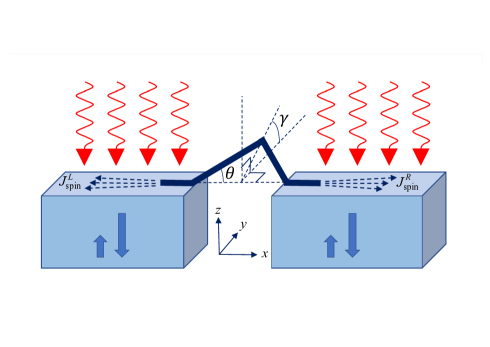
The SOI active weak-link device shown in Fig. 1 comprises a nanowire that bridges two bulk electronic reservoirs. The spin-orbit interaction described by Eq. (1) is restricted to the nanowire and has the effect of scattering the spins of electrons that pass through the wire. Following the approach developed in Refs. Shekhter.2013.2014x, ; Shekhter.2016x, ; Shekhter.2017, we will describe the transfer of electrons through the nanowire-based weak link with the help of a spin-dependent tunnel Hamiltonian. Hence, the total Hamiltonian of the system can be written as a sum of three parts,
| (2) |
where
| (3) |
are Hamiltonians that describe the electrons in the left and right leads. These electrons are characterized by the momentum quantum numbers and , respectively, and by the spin projection on the axis. We label the latter by , so that the spin projections are . The tunnel Hamiltonian is expressed in terms of the probability amplitudes for electron transmission through the wire,
| (4) |
These amplitudes have to be calculated taking the spin dynamics given by Hamiltonian (1) into account.
II Spin-biased electric weak link
Electronic transport through the weak link shown in Fig. 1 can be induced in a number of different ways. The standard method would be to apply a voltage bias across the link, so that the chemical potentials for electrons in the left and right reservoirs are shifted by a small amount with respect to each other. The result of such charge biasing is that excess charge of opposite polarity is accumulated on either side of the link, which leads to an electrical current through the link in a direction that counters the bias-induced charge imbalance.
Another method, which will be in focus here and which is illustrated in Fig. 1, is to arrange for the chemical potential to be different for the two possible projections of the electron spin along a certain axis. Such spin biasing can be achieved by illuminating the entire device with circularly-polarized microwave radiation of a frequency that enables electron spin-flip assisted photon absorption. This photonic pumping of the electronic spin creates an imbalance between the number of electrons with opposite spin projections on an axis defined by the direction of the radiation and leads to a spin-dependent shift in the chemical potentials for electrons with opposite spin projections. The magnitude of the shift, which extends throughout the device, depends on the intensity of the radiation and on the spin relaxation rate. If we assume that the SOI, which is restricted to the weak link, is the dominant spin relaxation mechanism the SOI becomes a source of a spin current, which flows out of the weak link into the two reservoirs and which counteracts the spin pumping. Referring to Fig. 1, we note that both the orientation of the plane that contains the weak link with respect to the pumped spin orientation and the bending angle of the link can be used to tune the generated spin current.
The spin bias can be defined by noting that for the electron spin reservoirs are described by Fermi-Dirac distributions with different chemical potentials,
| (5) |
where
| (6) |
and is the chemical potential of both leads at equilibrium. The spin current generated by electrons tunneling out of the SOI-active weak link can be obtained as the time derivative of the total spin, , of the electrons,
| (7) |
where
| (8) |
A straightforward calculation of the spin current (7) can be done using the tunnel Hamiltonian (1) to lowest order in perturbation theory Shekhter.2013.2014x . Then, one finds for the spin conductance (defined in analogy with the electrical conductance ) the relation
| (9) |
III Rashba spin splitting as a source of spin generation in SOI active weak link
In order to calculate the spin current given by Eq. (7) one needs to evaluate the electronic transmission amplitudes , which appear in the tunnel Hamiltonian (4), and specifically their dependence on the spin-orbit interaction as given by Eq. (1). In our simple model the weak link consists of two straight parts of equal length joined by a bend. Neglecting the momentum (but not the spin) dependence, the probability amplitude for an electron of energy to pass from, say, the left to the right lead can be written as a product of five factors,
| (10) |
Here is a 22 matrix in spin space, is the probability amplitude to tunnel from the wire to the left (right) lead and is the transfer matrix through the bend in the wire. In Ref. Shekhter.2017, the Green’s function for the straight segments of the wire, in which the SOI interaction takes place, was evaluated for a Hamiltonian of the form
| (11) |
A comparison with Eq. (1) shows that in the present case . Hence, from Eqs. (A12) and (A13) of Ref. Shekhter.2017, we conclude that
| (12) |
where we have used the short-hand notation , which is a measure of the strength of the SOI, and where
| (13) |
with , is the propagator on the left (right) segment in the absence of SOI. It follows that we can factor out the dependence on the SOI and write the amplitude given by Eq. (10) as
| (14) |
where
| (15) |
is the SOI-independent part and
| (16) |
contains the effect of the SOI.
In our geometry the axis is the spin quantization axis, and the bent wire lies in a plane that (i) contains the axis and (ii) is rotated by an angle away from the axis towards the axis. In the plane of the wire, the left (right) straight leg of the wire forms an angle (-) with the axis. In other words,
| (17) |
which means that we can write Eq. (16) in a matrix form,
| (18) |
where
| (19) |
and
| (20) |
Hence, the probability for a SOI-induced spin-flip transition is
| (21) |
The spin conductance can now be expressed in terms of the spin-flip probability as
| (22) |
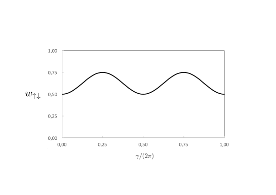
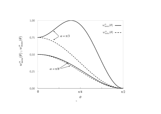
Equations (III) and (22) represent the main results of the paper. The strength of the SOI, characterized by the dimensionless parameter , determines the amount of photo-spintronic transduction that can be achieved by the studied Rashba spin-splitter device. The sensitivity of the effect to the geometry of the experimental set-up opens the possibility for tuning the device nanomechanically, by varying the angles and . The dependence of the spin conductance on these experimentally accessible device parameters is illustrated in Figs. 2 and 3.
The photo-spintronic transduction occurs even for a straight wire (i.e., when ). However, wire deformation provides a tool for a nanomechanical control of the generated spin current. Depending on the strength of SOI coupling , both a monotonic and a non-monotonic dependence of the dimensionless spin-conductance on mechanical deformations can be achieved.
Figure 2 illustrates that the dimensionless conductance, , is an oscillatory function of the angle . As is clear from Eq. (III), the maximal [minimal] value, [], of is achieved when the normal to the plane containing the nanowire weak link is perpendicular [parallel] to the spin quantization axis, i.e. when [ or ] and therefore [], independent of the values of and .
For a strong enough SOI, i.e., when , the largest possible value, , is reached when the bending angle is , where , as illustrated in Fig. 3. On the other hand, for the effect is smaller since then .
IV Conclusions
In this paper we have shown that a nanowire, in which the electrons are subjected to a spin-orbit interaction (SOI), can be used as a functional electric weak link between SOI-inactive leads and serve as an essentially point-like source of a spin-current induced by circularly-polarized microwave radiation. This spin current is not accompanied by a charge current. The possibility to concentrate such “pure” spin-currents at the nanometer length scale suggests novel spintronic devices.
Whether realistic applications are feasible crucially depends on how strong a photo-spintronic effect can be realized in practice, which in turn depends on the strength of the SOI that can be achieved. Consider, for instance, a single-wall carbon nanotube. Its strain-induced SO energy gap has been measured to be around 0.4 meV McEuen.2008 . Since , this value corresponds to m-1 for m/s. For nanowire lengths of the order of a m, can therefore be of order , which is large enough to allow the dimensionless spin conductance to be tuned near to its maximal value .
Acknowledgements.
This work was partially supported by the Swedish Research Council (VR), by the Israel Science Foundation (ISF) and by the infrastructure program of Israel Ministry of Science and Technology under contract 3-11173.References
- (1) D. D. Awschalom, L. C. Bassett, A. S. Dzurak, E. L. Hu, and J. R. Petta, Science 339, 1174 (2013).
- (2) R. I. Shekhter, O. Entin-Wohlman, and A. Aharony, Phys. Rev. Lett. 111, 176602 (2013); R. I. Shekhter, O. Entin-Wohlman and A. Aharony, Phys. Rev. B 90, 045401 (2014).
- (3) R. I. Shekhter, O. Entin-Wohlman, M. Jonson, and A. Aharony, Phys. Rev. Lett. 116, 217001 (2016).
- (4) R. I. Shekhter, O. Entin-Wohlman, M. Jonson, and A. Aharony, Low Temp. Phys. 43 (2) (2017) [Fiz. Niz. Temp. 43 (2) (2017)].
- (5) K. Koyama and H. Merz, Z. Physik B 20, 131 (1975); M. Wohlecke and G. Borstel, Phys. Stat. Solidi (b) 106, 593 (1981).
- (6) M. S. Rudner and E. I. Rashba, Phys. Rev. B 81, 125426 (2010); K. Flensberg and C. M. Marcus, Phys. Rev. B 81, 195418 (2010).
- (7) F. Kuemmeth, S. Ilani, D. C. Ralph, and P. L. McEuen, Nature 452, 448 (2008).