Thickness dependence of the resistivity of platinum-group metal thin films
Abstract
We report on the thin film resistivity of several platinum-group metals (Ru, Pd, Ir, Pt). Platinum-group thin films show comparable or lower resistivities than Cu for film thicknesses below about 5 nm due to a weaker thickness dependence of the resistivity. Based on experimentally determined mean linear distances between grain boundaries as well as ab initio calculations of the electron mean free path, the data for Ru, Ir, and Cu were modeled within the semiclassical Mayadas–Shatzkes model [Phys. Rev. B 1, 1382 (1970)] to assess the combined contributions of surface and grain boundary scattering to the resistivity. For Ru, the modeling results indicated that surface scattering was strongly dependent on the surrounding material with nearly specular scattering at interfaces with SiO2 or air but with diffuse scattering at interfaces with TaN. The dependence of the thin film resistivity on the mean free path is also discussed within the Mayadas–Shatzkes model in consideration of the experimental findings.
I Introduction
Finite size effects in the resistivity of metallic thin films or nanowires have been a topic of research for several decades both from a fundamental as well as an applied point of view. While the resistivity of bulk metals is dominated by phonon (and possibly impurity) scattering at room temperature, surface scattering can become dominant when the size of the thin films or nanowires is reduced 1 ; 2 ; ZB . In addition, grain sizes (i.e. mean linear distances between grain boundaries) in polycrystalline films or wires have typically been found to decrease for decreasing film thickness or wire diameter, which leads to an increasing contribution of grain boundary scattering in thin films or nanowires 3 ; 4 . Ultimately, when the structure size becomes of the order of a few nanometer, electron confinement effects will also alter the resistivity of metallic nanostructures Tesa ; NA ; ZB ; Mey ; Moors ; Hedge1 ; Jones ; Lanzillo ; Munoz . While this behavior is universally found in all metals, there is still controversy over the relative importance of the different additional scattering contributions even for the most studied material, Cu 7 ; 8 ; Maitre ; Marom ; Josell ; Sun1 ; Graham ; Sun2 ; Chawla1 ; Chawla3 , and only few comparative studies for different metals have been reported DeVries ; Tay ; Camacho .
From an applied point of view, the understanding of the resistivity of metals in small dimensions is crucial since metallic nanowires form the interconnect structures that are used in integrated microelectronic circuits. At present, the widths of scaled interconnect wires are of the order of 25 to 30 nm and are expected to reach dimensions of about 10 nm in the next decade. At such dimensions, surface and grain boundary scattering in Cu, the standard conductor material presently used in interconnects, dominate over phonon scattering, resulting in resistivities much larger than in the bulk 5 ; 6 ; 7 ; 8 ; Maitre and leading to a deterioration of the interconnect properties 9 ; 10 ; 11 ; Ceyhan . In addition, Cu-based interconnects require diffusion barriers and adhesion liners to ensure their reliability. Since their resistivity is typically much higher than that of Cu, their contribution to the wire conductance is often negligible. Barriers and liners are difficult to scale and may occupy a significant volume when the interconnect width approaches 10 nm, reducing the volume available for Cu. Therefore, alternative metals have recently elicited much interest as they could serve as a barrierless replacement for Cu. Among them, platinum-group metals (PGMs) have emerged as promising candidates due to the combination of low bulk resistivity, resistance to oxidation, and high melting point, which can be considered as a proxy for resistance to electromigration 12 ; 13 ; Kirou2 ; 14 .
The main quest for alternatives to Cu is motivated by the observation that the resistivity increase for thin films due to surface or grain boundary scattering depends on . Here, is the intrinsic mean free path (MFP) of the charge carriers in the metal and the characteristic length scale is the film thickness for surface scattering or the average linear distance between grain boundaries for grain boundary scattering 1 ; 2 ; ZB ; 3 ; 4 . Hence, metals with short MFPs should be inherently less sensitive to surface or grain boundary scattering for a given . As a result, such metals may show lower resistivities than Cu for sufficiently small dimensions despite their larger bulk resistivity 5 ; Zhang ; Naeemi . In addition, quantum effects for very small may also lead to such a behavior Simbeck ; Gao ; Lanzillo . However, such a crossover behavior has been elusive so far despite its strong interest for interconnect metallization.
In this paper, we discuss the thickness dependence of the resistivity of PGM (Ru, Pd, Ir, Pt) ultrathin films with thicknesses between 3 and 30 nm. We demonstrate that their resistivity exhibits a much weaker thickness dependence than that of Cu films in the same thickness range. As a result, for films thinner than about 5 nm, the resistivities of Ru and Ir films fall below that of Cu. The thickness dependence of the resistivity of Ru and Ir is then modeled using the analytical semiclassical Mayadas–Shatzkes approach. We demonstrate that, within the Mayadas–Shatzkes model, the shorter MFP of PGMs is indeed predominantly responsible for the resistivity crossover with respect to Cu. The data suggest that Ru, and Ir are promising metals for future interconnects in advanced technology nodes with interconnect widths below 10 nm ACSRuIC .
II Experimental and theoretical methods
All films were deposited by physical vapor deposition (PVD) at room temperature on Si (100). Prior to metal deposition, a 90 nm thick thermal oxide was grown on the Si wafers to ensure electrical isolation. Cu, Ru, and Ir films were deposited on 300 mm wafers in a Canon Anelva EC7800 system. In addition to films directly deposited on SiO2, Cu and Ru films were also grown in situ on 1.5 nm thick PVD TaN and capped by 1.5 nm thick PVD TaN. This was done to prevent the oxidation of the Cu surface, to avoid Cu diffusion into the underlying SiO2 during annealing, and to study the effect of the “cladding” material on the Ru thin film resistivity. Pt films were sputter deposited on small samples in a home build system using thin ( nm) Ti to promote adhesion. Pd films were obtained by e-beam evaporation using a Pfeiffer PLS 580 system on a thin TiN adhesion layer.
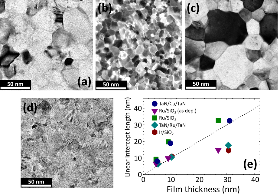
The thin film resistivity was calculated from sheet resistance measurements using KLA Tencor RS100 and Jandel 4-point probe systems as well as the film thickness measured by x-ray reflectivity (XRR). XRR was performed using Cu K radiation in a Bede MetrixL diffractometer from Jordan Valley or a Panalytical X’Pert diffractometer. Film thicknesses by XRR were cross-calibrated by Rutherford backscattering spectrometry (RBS) measurements using a 1.52 MeV He+ ion beam in a rotating random mode at a backscatter angle of 170∘. In all cases, the contribution of the adhesion layers to the sheet resistance was obtained by independent measurements and taken into account in the determination of the PGM thin film resistivity. The diffractometers mentioned above were also used to assess the film crystallinity using x-ray diffraction (XRD). Surface roughnesses were measured by atomic force microscopy (AFM) using a Bruker IconPT microscope. Lateral correlation lengths of the surface roughness were obtained from the autocorrelation function. The microstructure of the films was determined from plan-view transmission electron microscopy (TEM) images using Tecnai F30 and Titan3 G2 microscopes. Based on these images, the mean linear grain boundary intercept distance (the average linear distance between grain boundaries) was determined ASTM ; Abrams . Due to the almost columnar nature of the microstructure and their expected relatively weak contribution to the resistivity, grain boundaries parallel to the surface were neglected.
Electronic structures of the PGMs, Ru, Rh, Pd, Os, Ir, and Pt, as well as of Cu were obtained by first-principles calculations based on density functional theory as implemented in the Quantum Espresso package K8 . Projector augmented wave K9 potentials with the Perdew–Burke–Ernzerhof generalized gradient K10 approximation of the exchange-correlation functional have been used together with a Monkhorst–Pack k-point sampling grid and an energy cutoff of 80 Ry to ensure the convergence of the total energy differences (10 – 12 eV). The Fermi surface was determined from the calculated electron energy as a function of the wave vector k for each band with index . In addition, using the obtained Fermi surfaces and electronic densities of states, scattering times due to electron–phonon interactions have been calculated using standard first-order perturbation theory Allen . Details of these calculations can be found in Ref. 13 .
III Material properties and resistivity of platinum-group metal thin films
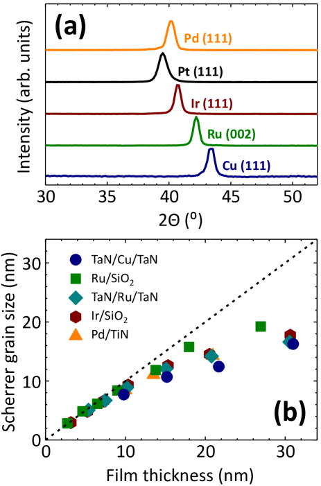
All films were polycrystalline as deposited. The - XRD patterns were consistent with the expected crystal structures of the stable phases (hcp for Ru, fcc for all other metals) with (partial) texture [(001) for Ru, (111) for other metals]. Post deposition annealing at 420 ∘C in forming gas for 20 min improved both the crystallinity and led to strong texturing [Fig. 1(a)]. The out-of-plane Scherrer crystallite size of annealed films [Fig 1(b)] was typically of the order of the film thickness for films up to about 15 nm and deviated slightly towards smaller values for thicker films. This indicates that the microstructure of the films was (nearly) columnar.
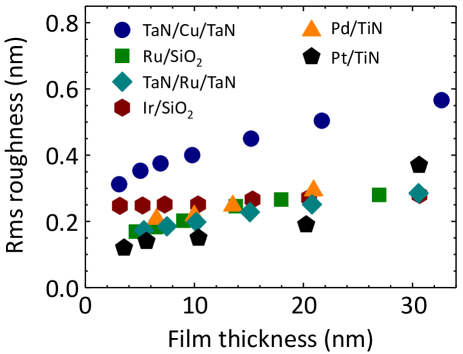
Figure 2 shows the root-mean-square (RMS) roughness of Cu (TaN/Cu/TaN), Ru (both Ru/SiO2 and TaN/Ru/TaN), Ir, Pd, and Pt films as a function of the film thickness after post deposition annealing at 420∘C. The roughness of the annealed films increased with increasing film thickness but remained below 0.4 nm even for 30 nm thick PGM films. Cu films were slightly rougher with RMS values of 0.5 to 0.6 nm for the thickest films. XRR measurements (not shown) indicated that the roughness of the top surface was very similar to that of buried interfaces (typically also 0.3 to 0.5 nm). The lateral correlation length of the surface roughness (obtained with Gaussian correlation statistics) was between 10 and 15 nm for all films with insignificant differences between materials/stacks and only little coarsening in the studied thickness range up to 30 nm.
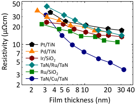
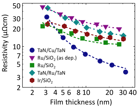
Figure 3 shows the resistivity of Cu (TaN/Cu/TaN), Ru (Ru/SiO2 and TaN/Ru/TaN), Pd, Ir, and Pt as a function of the film thickness. All films were annealed at 420 ∘C for 20 min in forming gas. Cu showed a strong increase with decreasing film thickness, as observed previously and ascribed to the combination of surface and grain boundary scattering. Note that the Cu resistivity values were close to the ones reported in the literature for scaled Cu interconnect lines of the same critical dimension ITRS ; PR .
By contrast, all PGM thin films showed a much weaker thickness dependence of the resistivity than Cu. For films with thicknesses of 10 nm and above, the resistivities were much higher than for Cu owing to the higher bulk resistivities of PGMs. However, for film thicknesses of about 5 nm and below, the resistivities of Ru and Ir became comparable and even lower than the resistivity of Cu. From a technological point of view, this resistivity crossover renders PGMs, in particular Ru and Ir highly interesting for scaled interconnects with critical dimensions of 10 nm and below, where the current combination of Cu, diffusion barriers, and adhesion liner layers may be outperformed by barrierless Ru or Ir metallization. Indeed, scaled Ru filled interconnect structures have already shown first promising results ACSRuIC demonstrating the prospects of these materials for future interconnect technology nodes.
From a more fundamental point of view, these data raise the question of the material dependence of the thin film scattering contributions, such as surface and grain boundary scattering. It has been asserted that a shorter electron MFP leads to a weaker thickness dependence of both surface and grain boundary scattering 5 ; Zhang ; Naeemi . However, to confirm this argument, effects of potentially different microstructures (e.g. the thickness dependence of the mean linear distance between grain boundaries) have to be understood.
IV Fermi surfaces and electron mean free paths of platinum-group metals
In a first step, we have computed the bulk electron MFPs of the PGMs as well as of Cu. The MFP in transport direction t of an electron with wave vector k is given by , where is the relaxation time of an electron with wave vector k and is the projection of the Fermi velocity on the transport direction. Here, is the Fermi energy of the band with index .
In a semiclassical approximation, the conductivity along the transport direction t can be expressed as Jacoboni ; Mahan
| (1) |
where is the (Fermi) distribution function, and has the dimension of an energy. The summation is carried out over the band index . At low temperature, . Assuming that the relaxation time is isotropic and does not depend on the band index, i.e. , one obtains 14
| (2) |
Here, the integration is carried out over the Fermi surface. Hence, the product of the relaxation time and the bulk resistivity depends only on the morphology of the Fermi surface. When the bulk resistivity is known, can be deduced and thus the MFP in the transport direction, . For polycrystalline materials, suitable averages can be obtained from the isotropic in combination with an average of over the relevant transport directions.
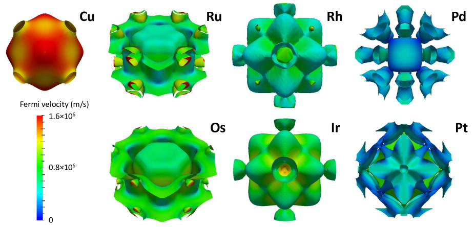
Using ab initio calculated Fermi surfaces (Fig. 4), was calculated for all PGMs as well as for Cu as a reference. Based on these values and experimental bulk resistivities Resistivity , relaxation times were then deduced. In addition, relaxation times due to electron–phonon scattering were directly calculated 13 ; Allen . Since all films were polycrystalline and textured, an effective Fermi velocity was obtained by averaging over transport directions perpendicular to [001] for the hcp metals (Ru, Os) and [111] for the fcc metals (Rh, Pd, Ir, Pt, and Cu). MFP values and were then calculated using and , respectively. The results are summarized in Tab. 1. Note that the resistivity of bulk hcp Ru and Os is anisotropic with the higher resistivity perpendicular to [001] Ru_aniso , i.e. along the transport direction of our textured films. The values are generally in good agreement with a previous report 14 .
As discussed above, metals with short MFPs may be less sensitive to surface or grain boundary scattering and thus may show a weaker thickness dependence of the resistivity than Cu 5 ; Zhang ; Naeemi . As indicated in Tab. 1, all PGMs show significantly shorter MFPs than Cu. Since the thin film resistivity for a given thickness or linear grain boundary distance also depends on the bulk resistivity, has been used as a figure of merit of a metal for the expected resistivity scaling at small dimensions 13 ; Kirou2 ; 14 . As shown in Tab. 1, all PGMs show higher figures of merit than Cu with Pt showing the highest value. However, due to a comparatively high bulk resistivity, Pt (as well as Pd and Os) may show benefits only for very small thicknesses or short linear grain boundary distances.
V Semiclassical thin film resistivity modeling
To gain further insight into the contributions of surface and grain boundary scattering, the resistivity of Ru, Ir and Cu was modeled using the semiclassical model developed by Mayadas and Shatzkes 4 . Despite recent advances in ab initio modeling Hedge1 ; Hedge2 ; Zhou ; Jones ; Lanzillo , the approach by Mayadas and Shatzkes remains the only tractable quantitative model for thin film resistivities in the studied thickness range up to 30 nm that contains both surface and grain boundary scattering. Here, transport is calculated within a Boltzmann framework using an isotropic Fermi surface. Band structure effects are however included in our calculations via an anisotropic mean free path, as discussed above.
The model also neglects confinement effects that are expected to further increase the resistivity. For nanowires, ab initio calculations have shown an orientation dependent increase of the resistivity although the magnitude of the increase varied between studies Hedge1 ; Hedge2 ; Jones ; Lanzillo ; Zhou . As a consequence, the thickness dependence of confinement effects in nanowires (and the transition to bulk-like behavior) cannot be considered as fully understood for (Cu) nanowires and even less so for (Cu or PGM) thin films, where confinement effects are expected to be weaker than for nanowires. Estimations of confinement effects within an anisotropic effective mass approximation (using anisotropic effective masses calculated from the above Fermi surfaces) lead to characteristic energies of the order of a few () meV for 5 nm thick Cu, Ru, and Ir films and the experimentally observed textures. These confinement energies are much smaller than the Fermi energy (and hence a large number of subbands are occupied) and even at room temperature. Recent ab initio results by Zhou et al. Zhou and Lanzillo Lanzillo for Cu suggest that expected confinement effects are still small compared to the experimentally observed increase of the thin film resistivity with respect to the bulk; therefore, grain boundary and surface scattering are expected to dominate over confinement effects in our thin films. We also note that we have observed no different trends for the thinnest films of 5 nm thickness and below, in the sense that fitting data subsets including thicker films only did not lead to significantly different fitting parameters. However, future work will be required to unambiguously identify the effect of band structure and confinement on the thin film resistivity, especially for film thicknesses far below 10 nm.
In the Mayadas–Shatzkes model, the resistivity of a thin film with thickness and average linear distance between grain boundaries (average linear intercept length RemGS ) is given by
| (3) |
with , , , and RemR . and are parameters that describe the surface and grain boundary scattering processes, respectively. The phenomenological surface specularity parameter varies between 0 for diffuse and 1 for specular scattering of charge carriers at the surface or interface; is the reflection coefficient () of a charge carrier at a grain boundary. In general, can take different values at the top and bottom interface, e.g. when the surface and interface roughnesses are strongly different, as described by the model of Soffer Soffer . However, given the observation that surface and buried interface roughnesses in the stacks considered here are low and very similar, we will assume that a single parameter can describe both interfaces of the metal films.
V.1 Film thickness dependence of the linear grain boundary distance
While surface scattering depends directly on the film thickness, grain boundary scattering depends on the average linear distance between grain boundaries, , along the transport direction. Therefore, a quantitative model of the thin film resistivity as a function of film thickness requires the knowledge of the thickness dependence of in polycrystalline films. Historically, it has often been assumed that is identical or proportional to the film thickness and this assumption has often been used to model the thickness dependence of the resistivity. However, it has been pointed out that such simple relations are generally not valid Marom_GS .
We have therefore experimentally determined the average linear grain boundary distance using the intercept method ASTM ; Abrams from plan-view transmission electron micrographs for 5, 10, and 30 nm thick Ru/SiO2 (as deposited and after annealing at 420 ∘C), TaN/Ru/TaN (annealed), Ir/SiO2 (annealed), and TaN/Cu/TaN (annealed) thin films. Figure 5 shows both sample TEM images as well as the deduced film thickness dependence of the mean linear grain boundary intercept length. While for TaN/Cu/TaN and annealed Ru/SiO2 the mean linear intercept length was close to the film thickness, other stacks clearly showed a saturating effect for nm thick films. Linear intercept lengths for in-between thicknesses were obtained by piecewise linear interpolation. Other more nonlinear interpolation schemes did not have any significant effects on the modeling results discussed below.
V.2 Semiclassical modeling results and discussion
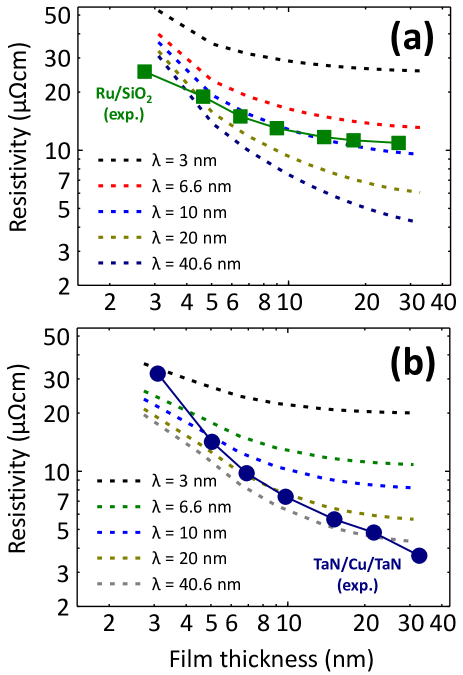
Figure 6 shows the experimental thickness dependence of the resistivities of Ru/SiO2, TaN/Ru/TaN, Ir/SiO2, and TaN/Cu/TaN, together with the best fits using the Mayadas–Shatzkes model in Eq. (3). All films were annealed at 420 ∘C for 20 min except for an additional data set of as deposited Ru/SiO2. To obtain best fits, the experimentally determined thickness dependences of the linear distance between grain boundaries for the different materials and stacks, as discussed in the previous section, were used. In addition, bulk electron MFPs obtained by ab initio calculations, (see Tab. 1), were employed in combination with experimental bulk resistivities. As discussed above, quantum confinement effects are difficult to quantify and have been neglected as they can still be expected to be small for the studied film thicknesses at room temperature except maybe for the very thinnest films (see also the discussion in Ref. Choi ). For Ru, the bulk resistivity has been reported to be anisotropic Ru_aniso . Since all films studied here showed strong (001) texture, the bulk in-plane resistivity (perpendicular to the hexagonal axis) has been used. Only and were used as adjustable parameters. In general, the model described well the thickness dependence of the thin film resistivity for all materials and stacks over the entire thickness range. The resulting parameters are listed in Tab. 2.
Using the Mayadas–Shatzkes model, the best fit to the data for Cu films (within a TaN/Cu/TaN stack) indicated that both surface () and grain boundary scattering () contribute to the thin film resistivity. The values of and fall well within the range of published values 7 ; 8 ; Maitre ; Marom ; Josell ; Sun1 ; Graham ; Sun2 ; Chawla1 ; Chawla3 . Moreover, they are in good agreement with a recent review Josell that concluded that the scattering at TaN/Cu interfaces is highly diffuse, in agreement with our results.
By contrast, fitted grain boundary reflection coefficients for Ru and Ir were larger than for Cu with to 0.58 for the different Ru stacks and for Ir/SiO2. Although grain boundary configurations, in particular the average misorientation angle of contiguous grains, can have an influence on the grain boundary resistance, as discussed below, a simple model of the material dependence of for polycrystalline films has been proposed by relating to the surface energy (and to the melting point) of the material Zhu . This is fully consistent with our observations that was larger for the more refractory Ru and Ir than for Cu. Moreover, our fitted values of for Ru and for Ir are in reasonable quantitative agreement with the predictions of this model of for Ru and for Ir Zhu . Note that the predicted value for Cu is , also in reasonable agreement with our results. Recently, Lanzillo calculated for twin boundaries in PGMs (Pt, Rh, Ir and Pd) by ab initio methods Lanzillo and found them to be higher than for Cu, in qualitative agreement with our results. It should however be noted that all such fitted values describe ”effective“ grain boundary reflection coefficients since the grain structures of the films certainly contain many different grain boundary structures. Moreover, the grain boundary transmission might also be affected by confinement effects for the thinnest films. For this reason, the quantitative understanding of grain boundary reflection coefficients both in Cu and PGMs will still require further work.
The fitted grain boundary coefficients of Ru/SiO2 showed a significant reduction upon annealing ( vs. ). This may be attributed to a reduction of the average misorientation of adjacent grains, as typically observed during recrystallization processes due to the preferred movement of large-angle grain boundaries Doherty ; recryst . It has been both calculated Cesar1 and experimentally observed Lu_Science ; Kim_GG_resistance ; Kim_GG_resistance2 for Cu that the resistance of boundaries between randomly oriented grains is much larger than that of coherent or coincidence grain boundaries. We speculate that a similar behavior also applies to Ru grain boundaries, leading to a reduction of upon annealing. The intermediate fitted value for the TaN/Ru/TaN stack is also in qualitative agreement with this argument since the observed small grain size even after annealing may be correlated with larger grain boundary resistances than for annealed large grain Ru on SiO2.
Interestingly, the best fits indicated that both Ru and Ir on SiO2 showed nearly specular surface scattering with . Hence, in those films, the Mayadas–Shatzkes model suggests that, despite their small thicknesses, surface scattering did not appear to contribute strongly to the resistivity. It has been calculated that the surface scattering coefficient for a given interface should be a strong function of both the magnitude (RMS) as well as its lateral correlation length of the surface roughness Moors ; FDD ; Ke ; RB . Although the Ru/SiO2 and Ir/SiO2 films were somewhat smoother than the TaN/Cu/TaN films (Fig. 2), the difference is small and the lateral correlations lengths are similar. Therefore, it appears unlikely that the difference between Ru/SiO2 as well as Ir/SiO2 and TaN/Cu/TaN was only due to differences in the physical surface properties. Thus, the electronic structure and the scattering potentials at the interface may contribute significantly Zahid .
Moreover, the fits indicated strongly diffuse scattering at Ru/TaN interfaces (as in TaN/Ru/TaN stacks) with . This implies that surface scattering depends less on the conducting metal (Ru vs. Cu) than on the cladding material of the thin film (SiO2/air vs. TaN). Note that surface roughnesses for TaN/Ru/TaN and Ru/SiO2 were almost identical. Similar observations have been made for Cu 7 ; Chawla_O2 ; Zheng . In particular, Rossnagel and Kuan 7 have observed that the surface scattering contribution to the thin film resistivity was lower in contact with oxides (SiO2, Ta2O5) than with TaN, very similar to our observations.
Several models for the surface specularity parameter have been reported in the literature FDD ; Ke ; RB ; Soffer ; FD_Ta_Cu ; Zahid that quantitatively link to the surface roughness and the intrinsic properties of the Fermi surface of the conducting material. However, only very few studies have considered the effect of the cladding material FD_Ta_Cu ; Zahid , which appears essential in view of the experimental results. Zahid et al. Zahid have studied the resistivity of Cu films surrounded by different metals using ab initio calculations and found that metals can both lower as well as increase with respect to a free Cu surface, depending on the difference of the density of states at the Fermi level of conducting metal (Cu) and the cladding atom at the interface. Although the density of states at the Ru/TaN interface has not yet been calculated, the bulk densities of states of Ru and TaN at the respective Fermi levels are rather similar. Additional work is thus needed to clarify the contributions of the properties of the conductor and the cladding material and its interface on the surface scattering parameter.
V.3 Relative contributions of surface and grain boundary scattering in the Mayadas–Shatzkes model and deviations from Matthiessen’s rule
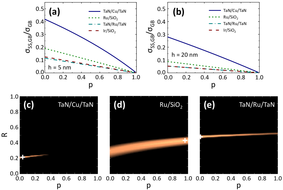
Equation (3) does not fulfill Matthiessen’s rule and the contributions of grain boundary and surface scattering can therefore not be separated. While the first term in Eq. (3), , describes grain boundary scattering independently of surface scattering, the second term, describes combined effects of surface and grain boundary scattering. Nonetheless, the ratio of the two terms can be evaluated and allows to shed some light on the relative importance of grain boundary and surface scattering within the Mayadas–Shatzkes model. Figure 7 shows the ratio of and as a function of the surface scattering parameter for TaN/Cu/TaN, Ru/SiO2, TaN/Ru/TaN, as well as Ir/SiO2 and film thicknesses of 5 nm [Fig. 7(a)] and 20 nm [Fig. 7(b)]. Experimental mean linear intercept lengths and surface scattering parameters corresponding to best fits were used. It should be noted that in Eq. (3), a ratio of corresponds to equal contributions of the two terms. If for all values of , the second term can be neglected and the thin film resistivity in the Mayadas–Shatzkes model is dominated by grain boundary scattering. However, due to the violation of Matthiessen’s rule, the opposite conclusion, namely the dominance of surface scattering for , is not necessarily valid.
The data indicate a general prevalence of grain boundary scattering over surface scattering within the Mayadas–Shatzkes model for all stacks even for the most diffusive case of since generally . Only for TaN/Cu/TaN (in particular for 5 nm film thickness), contributed strongly to the overall conductivity. By contrast, the contributions were weak for PGM containing stacks—even for fully diffusive surface scattering, as observed for TaN/Ru/TaN.
The different magnitudes of and have strong repercussions on the accuracy of the extracted and values. Figures 7(c)–(e) show the sum of squared errors (SSE) of the different fits as a function of the fitting parameters and for TaN/Cu/TaN, Ru/SiO2, and TaN/Ru/TaN. In general, due to the small contribution of , SSE minima were rather elongated along the -axis but well defined along the -axis. Generally, a rather weak gradient was visible along the elongated SSE minima towards the values reported in Tab. 2. Correlations between and were also visible that increase the otherwise very small errors in . Nonetheless, this resulted in much larger error bars (by about ) of as compared to .
This shows that the surface scattering specularity parameter of PGMs can therefore only approximately be determined by modeling of the thickness dependence of the resistivity within the Mayadas–Shatzkes model, at least for the film thicknesses and grain sizes considered here. However, the discussion above suggests that grain boundary scattering dominates the Ru and Ir thin film resistivities, even more so than for Cu, due to the much smaller MFP and that this holds independently of the exact value of . This also indicates that the absolute value of should not necessarily be taken as a measure whether surface scattering contributes significantly or not.
By contrast, the contribution of was much larger for TaN/Cu/TaN [Figs. 7(a) and (b)]. This can be linked to the long MFP of 40.6 nm and indicates that surface scattering cannot be simply neglected for thin Cu. Although both and are reduced with increasing MFP [via the dimensionless parameters and in Eq. (3)], appears more sensitive than , leading to an increasing prevalence of for large . In addition, the grain boundary reflection coefficient of Cu, was found to be much smaller than for PGMs (), which also leads to a weaker relative contribution of for Cu with respect to PGMs.
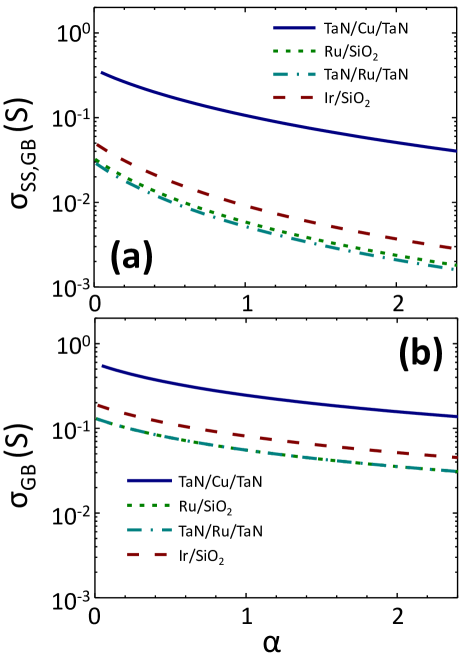
Among the PGMs, of Ru/SiO2 showed a much stronger dependence on [Figs. 7(a) and (b)] than TaN/Ru/TaN or Ir/SiO2. This can be linked to deviations from Matthiessen’s rule, as shown in Fig. 8. As pointed out by Mayadas and Shatzkes 4 , the (effective) MFP that determines surface scattering in a polycrystal (i.e. in presence of grain boundary scattering) is reduced over the bulk value by . This leads to a dependence of surface scattering on . The effect is illustrated in Fig. 8(a) for nm, which shows as a function . To make the curves more comparable, was assumed in all cases. For comparison, the dependence of on is also shown in Fig. 8(b). The data show that an increase of (i.e. stronger grain boundary scattering) leads to an decrease in that is generally faster than for . At nm, due to the combination of large grains and short MFP, for Ru/SiO2, much smaller than for TaN/Ru/TaN (), and Ir/SiO2 (), which leads to a relatively larger of Ru/SiO2 for a given value of . In practice however, the scattering at Ru/SiO2 and Ru/air interfaces was found to be nearly specular and the contribution of to the thin film resistivity was also negligible for Ru/SiO2.
V.4 Influence of the mean free path on the thickness dependence of the resistivity
Finally, we evaluate within the Mayadas–Shatzkes model the relative impact of the different material parameters (, , , ) on the slope of the thickness dependence of the thin film resistivity. It has been previously proposed that metals with a shorter MFP may show a much weaker thickness dependence of their thin film resistivity. However, this effect may potentially be complemented or domineered by other factors such as the material (stack) dependence of surface and grain boundary scattering coefficients as well as the thickness dependence of the mean linear grain boundary intercept length, which will in generally depend both on the material and the applied thermal budget.
To gain further insight in the importance of the electron MFP, we have calculated the expected thickness dependence of the resistivity of Cu or Ru as a function of the MFP, keeping constant as it is only a function of the Fermi surface morphology. The result, using the experimentally deduced parameters (, , and mean linear grain boundary intercept length) for Cu, is shown in Fig. 9(a). The data indicate that the overall slope of the resistivity vs. thickness curves shows a strong dependence on the MFP. Reducing the MFP to that of Ru (6.6 nm, see Tab. 1) while keeping constant ( m2) leads to both a slope and absolute resistivities that are close to what was experimentally observed for annealed Ru/SiO2 [Fig. 9(a)].
Conversely, as shown in Fig. 9(b), using the parameters obtained for annealed Ru/SiO2 (, , and average linear intercept between grain boundaries) and increasing the MFP to that of Cu (40.6 nm, see Tab. 1) while again keeping constant ( m2) leads to a slope almost identical to that experimentally observed for TaN/Cu/TaN. The residual differences stem from the material dependence of (see Tab. 1), , and (see Tab. 2), as well as from the different thickness dependence of the mean linear grain boundary intercept length, and are rather small. The larger deviations for the 3 nm thick films in both graphs can be ascribed within the Mayadas–Shatzkes model to the much stronger contribution of surface scattering to the Cu resistivity, which becomes significant only for such small thicknesses. As a whole, however, this confirms that the shorter MFP is the main root cause for the different thickness dependence of the resistivity of Cu and the PGMs.
VI Conclusion
In conclusion, we have studied the thickness dependence of the resistivity of ultrathin PGM films in the range between 3 and 30 nm. All studied PGMs (Ru, Pd, Ir, Pt) show a much weaker thickness dependence than Cu, the reference material. As a consequence, PGM thin film show comparable or even lower resistivities than Cu for film thicknesses of about 5 nm and below.
The thickness dependence of the resistivity of TaN/Cu/TaN, Ru/SiO2, TaN/Ru/TaN, and Ir/SiO2 was modeled using the Mayadas–Shatzkes model 4 and experimentally determined mean linear grain boundary intercept lengths as well as ab initio calculations of the MFP for bulk metals. Fitted grain boundary scattering coefficients for Ru and Ir ( to 0.5) were significantly higher than for Cu (), in good qualitative agreement with recent calculations Zhu ; Lanzillo . The model also found nearly specular scattering () was observed for both Ru and Ir on SiO2 but the interface scattering was much more diffuse () for TaN/Ru/TaN indicating that specular surface scattering is not an intrinsic material property of Ru. This behavior is currently not yet well understood owing to the lack of a general predictive theory for the material dependence of interface scattering. However, it should be noted that in all cases—irrespective of —surface scattering contributed only weakly to the overall resistivity, which was dominated by grain boundary scattering, except for the thinnest TaN/Cu/TaN films.
Simulations within the Mayadas–Shatzkes model showed that the much shorter MFP of Ru and Ir was indeed responsible for the much weaker thickness dependence of the thin film resistivity. This confirms earlier predictions 5 ; Zhang ; Naeemi and justifies the usage of as a figure of merit of alternative metals for beyond-Cu interconnects 13 ; 14 , in particular with respect to the the expected scaling behavior. Indeed, PGMs—and in particular Ru—have recently shown excellent prospects to replace Cu in future nanoscale interconnects with scaled widths of 10 nm and below ACSRuIC ; AM1 ; AM2 ; AM3 ; DuttaEDL .
Supplementary Material
See the supplementary material for the derivation of the correct definition of in Eq. (3).
Acknowledgements.
The authors would like to thank Sofie Mertens, Thomas Witters, and Karl Opsomer (imec) for the support of the PVD depositions, as well as Christian Witt (GlobalFoundries) for many stimulating discussions. Olivier Richard and Niels Bosman are acknowledged for the TEM imaging as well as Danielle Vanhaeren, Lien Landeloos, and Inge Vaesen (imec) for the AFM measurements. Johan Meersschaut is acknowledged for the RBS measurements. S.D. would like to thank Anamul Hoque, Kristof Peeters, Michiel Vandemaele, Christopher Gray, and Margo Billen (KU Leuven) for their assistance in the TEM image analysis. This work has been supported by imec’s industrial affiliate program on nano-interconnects.References
- (1) K. Fuchs, Math. Proc. Camb. Philos. Soc. 34, 100 (1938).
- (2) E. H. Sondheimer, Adv. Phys. 1, 1 (1952).
- (3) X.-G. Zhang and W. H. Butler, Phys. Rev. B 51, 10085 (1995).
- (4) A. F. Mayadas, M. Shatzkes, and J. F. Janak, Appl. Phys. Lett. 14, 345 (1969).
- (5) A. F. Mayadas and M. Shatzkes, Phys. Rev. B 1, 1382 (1970).
- (6) Z. Tešanović, M. V. Jarić, and S. Maekawa, Phys. Rev. Lett. 57, 2760 (1986).
- (7) N. Trivedi and N. W. Ashcroft, Phys. Rev. B 38, 12298 (1988).
- (8) A. E. Meyerovich and I. V. Ponomarev, Phys. Rev. 65, 155413 (2002).
- (9) K. Moors, B. Sorée, and W. Magnus, J. Appl. Phys. 118, 124307 (2015).
- (10) G. Hegde, M. Povolotskyi, T. Kubis, J. Charles, and G. Klimeck, J. Appl. Phys. 115, 123704 (2014).
- (11) S. L. T. Jones, A. Sanchez-Soares, J. J. Plombon, A. P. Kaushik, R. E. Nagle, J. S. Clarke, and J. C. Greer, Phys. Rev. B 92, (2015).
- (12) R. C. Munoz and C. Arenas, Appl. Phys. Rev. 4, 011102 (2017).
- (13) N. A. Lanzillo, J. Appl. Phys. 121, 175104 (2017).
- (14) S. M. Rossnagel and T. S. Kuan, J. Vac. Sci. Technol. B 22, 240 (2004).
- (15) J. J. Plombon, E. Andideh, V. M. Dubin, and J. Maiz, Appl. Phys. Lett. 89, 113124 (2006).
- (16) S. Maîtrejean, R. Gers, T. Mourier, A. Toffoli, and G. Passemard, Microelectron. Engin. 83, 2396 (2006).
- (17) H. Marom, J. Mullin, and M. Eizenberg, Phys. Rev. B 74, 045411 (2006).
- (18) D. Josell, S. H. Brongersma, and Z. Tőkei, Annu. Rev. Mater. Res. 39, 231 (2009).
- (19) T. Sun, B. Yao, A. P. Warren, K. Barmak, M. F. Toney, R. E. Peale, and K. R. Coffey, Phys. Rev. B 79, 041402(R) (2009).
- (20) R. L. Graham, G. B. Alers, T. Mountsier, N. Shamma, S. Dhuey, S. Cabrini, R. H. Geiss, D. T. Read, and S. Peddeti, Appl. Phys. Lett. 96, 042116 (2010).
- (21) T. Sun, B. Yao, A. P. Warren, K. Barmak, M. F. Toney, R. E. Peale, and K. R. Coffey, Phys. Rev. B 81, 155454 (2010).
- (22) J. S. Chawla, F. Gstrein, K. P. O’Brien, J. S. Clarke, and D. Gall, Phys. Rev. B 84, 235423 (2011).
- (23) J. S. Chawla and D. Gall, Appl. Phys. Lett. 94, 252101 (2009).
- (24) J. W. C. De Vries, Thin Solid Films 167, 25 (1988).
- (25) M. Tay, K. Li, and Y. Wu, J. Vac. Sci. Technol. B 23, 1412 (2005).
- (26) J. M. Camacho and A. I. Oliva, Microelectron. J. 36, 555 (2005).
- (27) P. Kapur, J. P. McVittie, and K. C. Saraswat, IEEE Trans. Electron Devices 49, 590 (2002).
- (28) W. Steinhögl, G. Schindler, G. Steinlesberger, and M. Engelhardt, Phys. Rev. B 66, 075414 (2002).
- (29) F. Chen and D. Gardner, IEEE Electron Device Lett. 19, 508 (1998).
- (30) P. Kapur, G. Chandra, J. P. McVittie, and K. C. Saraswat, IEEE Trans. Electron Devices 49, 598 (2002).
- (31) K. J. Kuhn, IEEE Trans. Electron Devices 59, 1813 (2012).
- (32) A. Ceyhan and A. Naeemi, IEEE Trans. Electron Devices 60, 4041 (2013).
- (33) C. Adelmann, L. G. Wen, A. P. Peter, Y. K. Siew, K. Croes, J. Swerts, M. Popovici, K. Sankaran, G. Pourtois, S. Van Elshocht, J. Bömmels, and Z. Tőkei, Proc. IEEE Int. Interconnect Technol. Conf., pp. 173 (2014).
- (34) K. Sankaran, S. Clima, M. Mees, C. Adelmann, Z. Tőkei, and G. Pourtois, Proc. IEEE Int. Interconnect Technol. Conf. pp. 193 (2014).
- (35) K. Sankaran, S. Clima, M. Mees, and G. Pourtois, ECS J. Solid State Sci. Technol. 4, N3127 (2015).
- (36) D. Gall, J. Appl. Phys. 119, 85101 (2016).
- (37) C. Pan and A. Naeemi, IEEE Electron Device Lett. 35, 250 (2013).
- (38) W. Zhang, S. H. Brongersma, O. Richard, B. Brijs, R. Palmans, L. Froyen, and K. Maex, Microelectron. Engin. 76, 146 (2004).
- (39) A. J. Simbeck, N. Lanzillo, N. Kharche, M. J. Verstraete, and S. K. Nayak, ACS Nano 6, 10449 (2012).
- (40) N. Gao, J. C. Li, and Q. Jiang, Appl. Phys. Lett. 103, 263108 (2013).
- (41) L. G. Wen, P. Roussel, O. Varela Pedreira, B. Briggs, B. Groven, S. Dutta, M. I. Popovici, N. Heylen, I. Ciofi, K. Vanstreels†, F. W. Østerberg, O. Hansen, D. H. Petersen, K. Opsomer, C. Detavernier, C. J. Wilson, S. Van Elshocht, K. Croes, J. Bömmels, Z. Tőkei, and C. Adelmann, ACS Appl. Mater. Interfaces 8, 26119 (2016).
- (42) ASTM E112-13, Standard Test Methods for Determining Average Grain Size, available at www.astm.org (ASTM International, West Conshohocken, PA, 2013).
- (43) H. Abrams, Metallography 4, 59 (1971).
- (44) P. Giannozzi, S. Baroni, N. Bonini, M. Calandra, R. Car, C. Cavazzoni, D. Ceresoli, G. L. Chiarotti, M. Cococcioni, I. Dabo, A. Dal Corso, S. Fabris, G. Fratesi, S. de Gironcoli, R. Gebauer, U. Gerstmann, C. Gougoussis, A. Kokalj, M. Lazzeri, L. Martin-Samos, N. Marzari, F. Mauri, R. Mazzarello, S. Paolini, A. Pasquarello, L. Paulatto, C. Sbraccia, S. Scandolo, G. Sclauzero, A. P. Seitsonen, A. Smogunov, P. Umari, and R. M. Wentzcovitch, J. Phys.: Condens. Matter 21, 395502 (2009).
- (45) P. E. Blöchl, Phys. Rev. B 50, 17953 (1994).
- (46) J. P. Perdew, K. Burke, and M. Ernzerhof, Phys. Rev. Lett. 77, 3865 (1996).
- (47) P. B. Allen, T. P. Beaulac, F. S. Khan, W. H. Butler, F. J. Pinski, and J. C. Swihart, Phys. Rev B 34, 4331 (1986).
- (48) International Technology Roadmap for Semiconductors – ITRS 2.0, available at www.itrs2.net, last accessed 10/24/2016.
- (49) P. Roussel, I. Ciofi, R. Degraeve, V. V. Gonzalez, N. Jourdan, R. Baert, D. Linten, J. Bömmels, G. Groeseneken, and A. Thean, Proc. IEEE Intern. Reliability Phys. Symp., IT-2 (2016).
- (50) C. Jacoboni, Theory of Electron Transport in Semiconductors (Springer, Berlin, Heidelberg, 2010).
- (51) G. D. Mahan, Many-Particle Physics (Springer, Boston, 2000).
- (52) J. Bass, Electrical Resistivity, Kondo and Spin Fluctuation Systems, Spin Glasses and Thermopower, in Landolt-Börnstein – Group III Condensed Matter, edited by K.-H. Hellwege and L. J. Olsen, Vol. 15A, SpringerMaterials, available at dx.doi.org/10.1007/b29240 (Springer Verlag, Berlin, Heidelberg, 1983).
- (53) E. M. Savitskii, P. V. Gel’d, V. E. Zinov’ev, N. B. Gorina, and V. P. Polyakova, Sov. Phys. Dokl. 21, 456 (1976); N. V. Volkenshteyn, V. Ye. Startsev, V. I. Cherepanov, V. M. Azhazha, G. P. Kovtun, and V. A. Yelenskiy, Phys. Met. Metallogr 45, 54 (1978).
- (54) Y. Zhou, S. Sreekala, P. M. Ajayan, and S. K. Nayak, J. Phys.: Condens. Matter 20, 095209 (2008).
- (55) G. Hegde, R. C. Bowen, and M. S. Rodder, Appl. Phys. Lett. 109, 193106 (2016).
- (56) Although Mayadas and Shatzkes in Ref. 4 employ the term grain size, their derivation of Eq. (3) is actually based on the average linear distance between grain boundaries, i.e. the mean linear grain boundary intercept length. While average grain size and mean linear intercept length are typically found to be proportional to each other, the proportionality constant deviates significantly from unity and depends on the grain size distribution. See e.g., A. Thorvaldsen, Acta Materialia 45, 595 (1997).
- (57) The definition of in Mayadas and Shatzkes, Ref. 4 , misses a factor of 2. For the derivation of the correct definition of , see the supplementary material. Our results can be compared to studies based on the original definition of by using .
- (58) S. B. Soffer, J. Appl. Phys. 38, 1710 (1967).
- (59) H. Marom, M. Ritterband, and M. Eizenberg, Thin Solid Films 510, 62 (2006).
- (60) D. Choi, X. Liu, P. K. Schelling, K. R. Coffey, and K. Barmak, J. Appl. Phys. 115, 104308 (2014).
- (61) Y. F. Zhu, X. Y. Lang, W. T. Zheng, and Q. Jiang, ACS Nano 4, 3781 (2010).
- (62) R. D. Doherty, D. A. Hughes, F. J. Humphreys, J. J. Jonas, D. Juul Jensen, M. E. Kassner, W. E. King, T. R. McNelley, H. J. McQueen, and A. D. Rollett, Mater. Sci. Engin. A 238, 219 (1997).
- (63) F. J. Humphreys and M. Hatherly, Recrystallization and Related Annealing Phenomena, 2nd ed. (Elsevier, Oxford, 2004).
- (64) M. César, D. Liu, D. Gall, and H. Guo, Phys. Rev. Applied 2, 44007 (2014).
- (65) L. Lu, Y. Shen, X. Chen, L. Qian, and K. Lu, Science 304, 422 (2004).
- (66) T.-H. Kim, X.-G. Zhang, D. M. Nicholson, B. M. Evans, N. S. Kulkarni, B. Radhakrishnan, E. A. Kenik, and A.-P. Li, Nano Lett. 10, 3096 (2010).
- (67) T.-H. Kim, D. M. Nicholson, X.-G. Zhang, B. M. Evans, N. S. Kulkarni, E. A. Kenik, H. M. Meyer, B. Radhakrishnan, and A.-P. Li, Jpn. J. Appl. Phys. 50, 08LB09 (2011).
- (68) B. Feldman, R. Deng, and S. T. Dunham, J. Appl. Phys. 103, 113715 (2008).
- (69) Y. Ke, F. Zahid, V. Timoshevskii, K. Xia, D. Gall, and H. Guo, Phys. Rev. B 79, 155406 (2009).
- (70) J. M. Rickman and K. Barmak, J. Appl. Phys. 112, 13704 (2012).
- (71) F. Zahid, Y. Ke, D. Gall, and H. Guo, Phys. Rev. B 81, 045406 (2010).
- (72) J. S. Chawla, F. Zahid, H. Guo, and D. Gall, Appl. Phys. Lett. 97, 132106 (2010).
- (73) P. Y. Zheng, R. P. Deng, and D. Gall, Appl. Phys. Lett. 105, 131603 (2014).
- (74) B. Feldman and S. T. Dunham, Appl. Phys. Lett. 95, 222101 (2009).
- (75) X. Zhang, H. Huang, R. Patlolla, W. Wang, F. W. Mont, J. Li, C.-K. Hu, E. G. Liniger, P. S. McLaughlin, C. Labelle, E. T. Ryan, D. Canaperi, T. Spooner, G. Bonilla, and D. Edelstein, Proc. IEEE Int. Interconnect Technol. Conf., pp. 31 (2016).
- (76) L. G. Wen, C. Adelmann, O. Varela Pedreira, S. Dutta, M. Popovici, B. Briggs, N. Heylen, K. Vanstreels, C. J. Wilson, S. Van Elshocht, K. Croes, J. Bömmels, and Z. Tőkei, Proc. IEEE Int. Interconnect Technol. Conf., pp. 34 (2016).
- (77) J. S. Chawla, S. H. Sung, S. A. Bojarski, C. T. Carver, M. Chandhok, R. V. Chebiam, J. S. Clarke, M. Harmes, C. J. Jezewski, M. J. Kobrinski, B. J. Krist, M. Mayeh, R. Turkot, and H. J. Yoo, Proc. IEEE Int. Interconnect Technol. Conf., pp. 63 (2016).
- (78) S. Dutta, S. Kundu, A. Gupta, G. Jamieson, J. F. Gomez Granados, J. Bömmels, C. J. Wilson, Z. Tőkei, and C. Adelmann, IEEE Electron Device Lett. 99, in print, DOI: 10.1109/LED.2017.2709248 (2017).
| ( ms) | (fs) | ( cm) | (fs) | ( m/s) | (nm) | (nm) | ( S/m2) | |
|---|---|---|---|---|---|---|---|---|
| Cu | 6.36 | 23.2 | 1.71 | 37.2 | 10.92 | 25.3 | 40.6 | 1.4 |
| Ru | 6.68 | 8.6 | 7.6 | 8.8 | 7.47 | 6.4 | 6.6 | 2.0 |
| Rh | 5.18 | 10.3 | 4.8 | 10.8 | 6.92 | 7.1 | 7.5 | 2.8 |
| Pd | 11.00 | 19.9 | 10.7 | 10.3 | 3.18 | 6.3 | 3.3 | 2.8 |
| Ir | 4.77 | 2.7 | 5.2 | 9.2 | 8.83 | 2.4 | 8.1 | 2.4 |
| Os | 6.81 | 9.1 | 10.0 | 6.8 | 8.39 | 7.6 | 5.7 | 1.8 |
| Pt | 5.64 | 8.6 | 10.6 | 5.3 | 5.20 | 4.5 | 2.8 | 3.4 |
| (nm) | ( cm) | ||||
|---|---|---|---|---|---|
| Ru/SiO2 (as deposited) | 0 | 6.6 | 7.6 | 0.99 | |
| Ru/SiO2 (annealed) | 6.6 | 7.6 | 0.92 | ||
| TaN/Ru/TaN (annealed) | 6.6 | 7.6 | 0.99 | ||
| Ir/SiO2 (annealed) | 8.1 | 5.2 | 0.95 | ||
| TaN/Cu/TaN (annealed) | 40.6 | 1.71 | 0.99 |