Controlling evanescent waves using silicon photonic all-dielectric metamaterials for dense integration
Abstract
Ultra-compact, densely integrated optical components manufactured on a CMOS-foundry platform are highly desirable for optical information processing and electronic-photonic co-integration. However, the large spatial extent of evanescent waves arising from nanoscale confinement, ubiquitous in silicon photonic devices, causes significant cross-talk and scattering loss. Here, we demonstrate that anisotropic all-dielectric metamaterials open a new degree of freedom in total internal reflection to shorten the decay length of evanescent waves. We experimentally show the reduction of cross-talk by greater than 30 times and the bending loss by greater than 3 times in densely integrated, ultra-compact photonic circuit blocks. Our prototype all-dielectric metamaterial-waveguide achieves a low propagation loss of approximately dB/cm, comparable to those of silicon strip waveguides. Our approach marks a departure from interference-based confinement as in photonic crystals or slot waveguides, which utilize nanoscale field enhancement. Its ability to suppress evanescent waves without substantially increasing the propagation loss shall pave the way for all-dielectric metamaterial-based dense integration.
pacs:
Valid PACS appear hereIntroduction
One of the long-standing goals of nanophotonics is the integration of electronic and photonic circuitry on a single CMOS chip for applications ranging from information processing and data centers to massively parallel sensing Jalali and Fathpour (2006); Bogaerts et al. (2005); Nagarajan et al. (2005); Soref (2006); Kim et al. (2017); Chrostowski and Hochberg (2015); Dai et al. (2012); Heck et al. (2013); Luo et al. (2014); Momeni et al. (2009); Shen et al. (2017). This necessarily requires miniaturization with low power consumption in optical interconnects, active as well as passive photonic devices. There are two major figures of merit in designing photonic devices for a densely integrated circuit. One is the cross-talk, which occurs due to the field overlap of two adjacent photonic waveguides, and the second is the radiation loss at sharp bends which limits the integration density Chrostowski and Hochberg (2015).
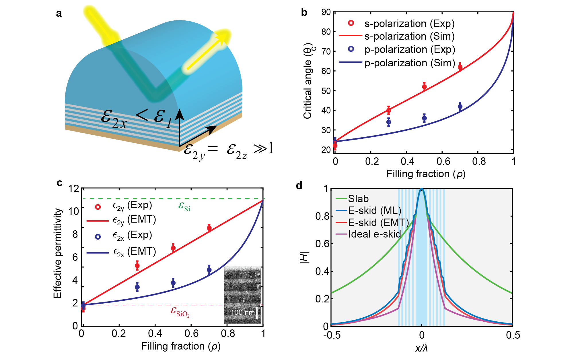
Plasmonic waveguides can strongly reduce cross-talk and bending loss due to the sub-diffraction nature of light coupling to the free electrons of metals Dionne et al. (2006); Oulton et al. (2008); Gramotnev and Bozhevolnyi (2010); Alù and Engheta (2009); Kim and Qi (2015a, b); Raza et al. (2014); Kinsey et al. (2015). However, the large ohmic loss of metals restricts the application of plasmonic structures for photonic integration Khurgin (2015, 2017). Over the last decade, many efforts have been made to miniaturize photonic components using all-dielectric structures Jahani and Jacob (2016); Priolo et al. (2014); Kuznetsov et al. (2016); Staude and Schilling (2017); Chang-Hasnain and Yang (2012); Krasnok et al. (2012); Baranov et al. (2017); Liu et al. (2016); Arbabi et al. (2015, 2016); Khorasaninejad et al. (2016); Shen et al. (2015a); Piggott et al. (2015); Hafezi et al. (2013); Slobozhanyuk et al. (2016). Figure 1 illustrates a few classes of dielectric waveguides for light confinement in photonic chips. Strip waveguides, the most common type of waveguides for routing light in a silicon chip, are composed of a silicon channel surrounded by silicon oxide Chrostowski and Hochberg (2015) (Fig. 1a). Due to the high contrast between the refractive index of the core and the cladding, light is confined inside the core as a result of total internal reflection. However, the mode size is seen to increase as we reduce the core size which hampers the use of strip waveguides to further miniaturize photonic circuits Jahani and Jacob (2014). Photonic crystal waveguides can confine light inside a line defect due to Bragg reflection Joannopoulos et al. (2008); Benisty et al. (1999); Hsu et al. (2013) (Fig. 1b). These waveguides perform efficiently at very sharp bends Mekis et al. (1996), however, the integration density is limited as the periodicity of Bragg reflectors is on the order of the wavelength and it cannot be perturbed by another waveguide nearby Dai et al. (2007). Additionally, slot waveguides have been proposed to confine light inside a sub-wavelength low index gap surrounded by high index dielectric rods Almeida et al. (2004) (Fig. 1c). To satisfy the continuity of the normal component of the displacement current at the high contrast interface, the electric field peaks inside the gap, leading to light confinement but at the cost of skin-depth expansion in the cladding. This causes cross-talk between adjacent waveguides and radiation loss at sharp bends in dense photonic integrated circuits.
 |
Several alternative approaches inspired from atomic physics Song et al. (2015); Mrejen et al. (2015), transformation optics Gabrielli et al. (2012), and inverse-design algorithms Shen et al. (2015b, 2016) have also been proposed to minimize the cross-talk and the bending loss. However, these techniques add design complexity often required modification of the core as well as cladding Gabrielli et al. (2012). They are not implementable on a large scale and cause propagation loss fundamentally limiting device performance. Thus, a new low-loss and scalable platform is needed for CMOS foundry compatible dense photonic integration with low cross-talk and reduced bending loss.
In this paper, we demonstrate a platform which is fundamentally different from the existing approaches for designing CMOS compatible, ultra-compact, and low loss waveguides using all-dielectric anisotropic metamaterials. Our approach works based on photonic skin-depth engineering of evanescent waves in the cladding using a recently proposed degree of freedom in total internal reflection (TIR) Jahani and Jacob (2014, 2015a). To describe the light confinement mechanism in our waveguides, first, we experimentally demonstrate the phenomenon of relaxed-total internal reflection in anisotropic metamaterials. These relaxed conditions allow the control of evanescent wave decay which is the fundamental origin of cross-talk and bending loss in silicon photonic devices. As illustrated in Fig. 1d, we use these anisotropic metamaterials as a cladding for on-chip dielectric waveguides fabricated on a monolithic silicon-on-insulator (SOI) platform. As a result, cross-talk is reduced down to -30 dB in the photonic circuit. Furthermore, we use a transformation optics approach to show that the radiation loss at sharp bends is strongly influenced by the skin-depth in the cladding. We experimentally show that the anisotropic metamaterial cladding can simultaneously reduce the bending loss at sharp bends up to 3 times compared to conventional silicon strip waveguides. We clarify the counter-intuitive nature of light confinement in our approach compared to existing photonic crystal, slot waveguide, and graded index waveguide methods Joannopoulos et al. (2008); Almeida et al. (2004); Bock et al. (2010); Halir et al. (2015); Yang et al. (2008); Levy et al. (2005). Our work shows that all-dielectric anisotropy on-chip presents a scalable route to simultaneously improve cross-talk and bending loss with propagation loss as low as dB/cm. For completeness, we show the improvements in figures of merit of our achieved platform with recent state-of-the-art photonic designs (See Table 1).
 |
| Reference | Cross-talk | Propagation loss |
|---|---|---|
| Superlattice Song et al. (2015) | -20 dB | dB/cm |
| Adiabatic elimination Mrejen et al. (2015) | -21.9 dB | N/A |
| Inverse design Shen et al. (2016) | -22.9 dB | dB/cm |
| Dissimilar waveguides Murray et al. (2015) | -20 dB | N/A |
| Sinusoidal waveguides Zhang et al. (2015) | -26.8 dB | dB/cm |
| This work (e-skid) | -30 dB | 3.67 dB/cm |
It is seen that the cross-talk is significantly reduced in e-skid waveguides at the negligible cost of propagation loss in comparison with other approaches.
Results
Relaxed total internal reflection. We demonstrate that only a single component of the dielectric tensor governs total internal reflection (TIR) in anisotropic media opening a new degree of freedom to control evanescent waves. In conventional TIR, if and the incident angle is greater than the critical angle (), light is reflected back to the first medium and decays evanescently in the second medium. However, we have recently found that the TIR conditions at the interface of an isotropic and an anisotropic dielectric are relaxed to Jahani and Jacob (2014, 2015b):
| (2) | |||
| (4) |
where is the permittivity tensor of the second medium, and the interface between the two media lies on the plane. As a result, the critical angle for s and p polarizations differ:
| (6) | |||
| (8) |
We emphasize that these relaxed conditions for p polarized incident light allow us to arbitrarily increase or decrease the permittivity in the direction while still preserving TIR. This hitherto un-utilized degree of freedom can thus be used to control the skin depth of evanescent waves. If , evanescent waves decay faster than in vacuum allowing for strong light confinement inside dielectric waveguides Jahani and Jacob (2014, 2015a). In this limit, note that the averaged index in anisotropic medium 2 can be larger than the refractive index in isotropic medium 1 yet the light will be totally reflected above the critical angle.
 |
 |
We implement this anisotropy using Si/SiO2 multilayers with subwavelength thicknesses (Fig. 2a) at the telecommunication wavelength ( nm). Figure 2 highlights the contrast between relaxed-TIR and conventional TIR, showing the measured light reflection at the interface of a hemi-cylindrical Si prism and the anisotropic multilayer metamaterial. The periodicity of the multilayer is nm and 5 periods have been deposited on the prism. The Maxwell-Garnett effective medium theory (EMT) Milton (2002) predicts that the multilayer with subwavelength periodicity demonstrates strong anisotropy Jahani and Jacob (2014); Herzig Sheinfux et al. (2014); Halir et al. (2016); Sayem et al. (2016); Gomis-Bresco et al. (2017) at the operating wavelength ( and where is the fill fraction of silicon). Note we are in the effective medium metamaterial limit () away from the photonic crystal regime (). Reflection occurs on two interfaces, the primary silicon-metamaterial interface and the secondary metamaterial-air interface. We have deposited a thin tungsten layer on top of the multilayer metamaterial to attenuate the unwanted reflection from the secondary metamaterial/air interface. Figure 2b displays different measured critical angles for s and p polarizations. Various samples with different fill fractions have been fabricated. As deviates from 0 and 1, the multilayer displays effective anisotropy and the critical angle for s and p polarized incidences are separated in agreement with relaxed-TIR theory in equation (6). The effective permittivity of the multilayer structure (extracted from the critical angle) shows strong anisotropy and is in good agreement with EMT (Fig. 2c). It is clearly seen that the critical angle depends on only one component of the permittivity tensor for each polarization irrespective of the fill-fraction. With the extra degree of freedom afforded by the other components of the dielectric tensor, this anisotropic structure can be used as a cladding for conventional dielectric waveguides to control the evanescent waves and skin-depth in the cladding Jahani and Jacob (2014); Li et al. (2017). Figure 2d displays the effect of the multilayer anisotropic cladding on reducing of the evanescent wave skin-depth as compared to a conventional slab waveguide. Note that this evanescent wave engineering approach in extreme skin-depth (e-skid) waveguides is due to the fast variation of the evanescent fields in a subwavelength high-index-contrast super-lattice (Fig. 2d). This is fundamentally different from other light confinement strategies which function on interference of propagating waves (photonic crystals) or field enhancement in a slot Joannopoulos et al. (2008); Almeida et al. (2004); Halir et al. (2015); Yang et al. (2008); Levy et al. (2005).
On-chip e-skid waveguides. To impact the field of silicon photonics, the one-dimensional e-skid waveguide (Fig. 2d) has to be implemented on an SOI platform. This places stringent restrictions on monolithic fabrication, minimum feature sizes, and deviations in field profiles due to quasi-2D behavior. Our design to adapt relaxed TIR and skin-depth engineering () on-chip is shown in Fig. 3. Here the conventional quasi-2D strip waveguide is surrounded by a cladding made of alternating vacuum-silicon sub-wavelength ridges which achieves strong anisotropy ( and ). Our goal is to confine the TE-like mode (its dominant electric field component is ) used in conventional silicon strip waveguides. Since the TM-like mode is polarized in the direction, the electric field does not probe/feel the anisotropy of the cladding. Hence, the metamaterial cladding does not play any role in TM-mode confinement. For more details about the polarization effect, see Supplementary Figures 6 and 7.
Figure 3a emphasizes the counter-intuitive nature of the confinement caused by anisotropic media which beats the confinement of conventional high index contrast interface consisting of silicon surrounded by vacuum (blue curve in Fig. 3a). As it is seen in Fig. 3a, if we increase the index of the cladding only in the direction while the index in the other directions are fixed, the evanescent wave decays faster in the cladding and the skin-depth reduces drastically. Note, the average cladding index increases but the mode decay length decreases. This behavior is in fundamental contrast to confinement in conventional strip waveguides with isotropic claddings or graded index claddings Levy et al. (2005) where decreasing the contrast between the core index and cladding index results in slow decay of evanescent waves, not faster decay Jahani and Jacob (2015a).
Figure 3b shows the field profile of a practical e-skid waveguide with the multilayer metamaterial cladding (). We can see the practical multilayer cladding shows strong effective anisotropy to ensure the fast decay of the evanescent wave in the cladding. The 2D field profiles in a plane perpendicular to the propagation direction and comparison of the practical e-skid waveguide with a homogeneous anisotropic cladding are shown in Fig. 3c and 3d. A good agreement with the effective medium approximation is seen. Figure 3e-3h illustrate the effective modal index and the decay constant in the cladding for a wide range of core sizes and the fill fractions of silicon in the multilayer cladding. First, a strong agreement is seen between EMT and practical multilayer structures indicating that the cladding indeed achieves effective all-dielectric anisotropy. Secondly, the effective modal index is below the core index indicative of relaxed total internal reflection as the mechanism of confinement. As expected, simulations prove that the primary role of the on-chip multi-layer cladding is to increase the decay constant of evanescent waves (), as shown in Figs. 3f and 3h, and it does not significantly change the effective modal index of propagating waves (), as shown in Figs. 3e and 3g. It is seen that the largest decay constant is achieved at where the strongest anisotropy is attained. Note that corresponds to the case of no cladding. We also emphasize that the power in the core is not compromised by the presence of the skin-depth engineering cladding and increased anisotropy causes an enhancement in power confinement.
 |
This light confinement strategy in e-skid waveguides is fundamentally different from that in photonic crystal waveguides. Our multilayer structures function in the deep subwavelength limit (), not the photonic crystal limit () and the performance of the e-skid waveguide is independent of the multilayer periodicity or disorder (see Supplementary note 2). Furthermore, there are no Dyakonov wave solutions in e-skid waveguides as the optical axis of the anisotropic cladding is perpendicular to the interface and the direction of propagation Dyakonov (1988); Takayama et al. (2009, 2014); Jahani and Jacob (2016); Polo and Lakhtakia (2011); Talebi et al. (2016). It is also important to note that the main goal of the anisotropic multilayer cladding is to control the decay constant of evanescent waves on-chip, not to achieve birefringence in the effective modal index of propagating waves as achieved previously in sub-wavelength grating structures Chang-Hasnain and Yang (2012); Bock et al. (2010); Halir et al. (2015); Boroojerdi et al. (2016), multi-slotted waveguides Yang et al. (2008), or nonlinear phase matching applications Fiore et al. (1998).
 |
Cross-talk in e-skid waveguides. The skin-depth of evanescent waves is the fundamental origin of cross-talk between waveguides that hinders dense photonic integration. Cross-talk, or power coupling between photonic devices, arises due to the perturbation of the optical mode when the evanescent tail of one waveguide overlaps with a nearby waveguide. However, if we control the skin-depth in the cladding, we can reduce the perturbation due to the adjacent waveguide, subsequently reducing the cross-talk to surpass the integration limit in current silicon photonics.
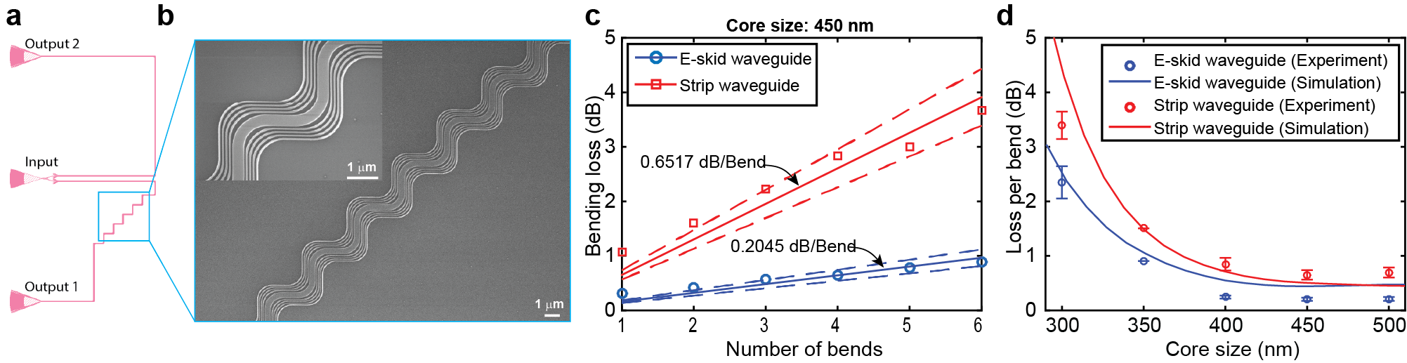
We now demonstrate this drastic reduction in the cross-talk made possible with the anisotropy in the cladding (Fig. 4a). The top view image of coupled e-skid waveguides fabricated on an SOI chip is shown in Fig. 4b. The power exchanged between two identical lossless coupled waveguides is:
| (9) |
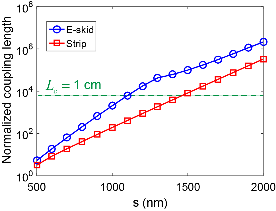
where is the input power, is the distance for which the two waveguides are coupled, and is the coupling length. Note is defined such that if the waveguides are coupled for a distance , complete power transfer occurs from the first waveguide to the adjacent waveguide. Figure 4c illustrates the experimental setup to measure the coupling length. Light is in-coupled to the first waveguide through the grating coupler Wang et al. (2014) and the second waveguide is coupled to the first waveguide over a distance of . The center-to-center separation between the two waveguides is only 1000 nm. The output power of the two waveguides is out-coupled by the two grating couplers at the ends of each waveguide. Note that we can ignore the propagation loss in this experiment as the total length does not exceed a few hundred microns whereas the propagation loss is 3.67 dB/cm at the operating wavelength nm (see Supplementary note 6 for details about the characterization of the propagation loss). The ratio between the measured powers for strip waveguides and e-skid waveguides are shown in Fig. 4d. This highlights that the analytical expression () matches the experimental data. It is clearly seen that the coupled power to the second waveguide is almost two orders of magnitude lower for the e-skid waveguide. The measured and simulated CST Microwave Studio coupling length normalized to the wavelength for different core sizes is plotted in Fig. 4e for waveguides with the same separation distance of 1000 nm. It is seen that the coupling length for the TE-like mode of e-skid waveguides is an order of magnitude higher than that for strip waveguides allowing miniaturization of photonic integrated circuits without considerable cross-talk between the waveguides. Note that increasing the core size in conventional strip waveguides, which corresponds to higher power confinement inside the core, does not guarantee the reduction in cross-talk (unshaded region Fig. 4e) as the evanescent tails are not controlled. These drastically increased are due to the reduced skin-depth with a higher anisotropy, reducing the waveguide cross-talk significantly in comparison with other dielectric structures which have been proposed to reduce the cross-talk (Table 1). Note that since the TM-like mode has a negligible electric field component in the direction, it does not probe/feel the dielectric anisotropy of the cladding. As expected, this results in higher cross-talk for TM-modes compared to strip waveguides (see Supplementary Figures 6 and 7 for more details about the polarization effect and the proposed design to control the skin-depth of the TM-like mode).
Bending loss in e-skid waveguides. The critical phenomenon of bending loss Heiblum and Harris (1975); Vlasov and McNab (2004); Marcatili (1969) can also be reduced by adding the anisotropic metamaterial cladding. The counterintuitive connection of bending loss and skin-depth is revealed by an approach adapted from transformation optics Heiblum and Harris (1975); Han et al. (2013). Here, we consider a curved waveguide in the plane with a bend and a bending radius of (). The center of the curved waveguide is at the origin (Figs. 5b and 5d (inset)). If we apply the transformation: Heiblum and Harris (1975); Han et al. (2013), the curved waveguide is mapped to a straight waveguide in the plane (Figs. 5b and 5d). This causes the refractive index of the transformed waveguide to become inhomogeneous in the new coordinate system as Heiblum and Harris (1975); Han et al. (2013): , where is the refractive index of the straight waveguide as shown in Figs. 5a and 5b. Bending loss or radiative power leakage from the core occurs in this straight inhomogeneous index waveguide when the local index of the cladding exceeds the effective modal index (). Hence, if we suppress the field near and beyond this radiation condition point (Fig. 5b and 5d), we can reduce the bending loss. Note that due to the spatial transformation of coordinates, the electromagnetic fields are also transformed causing the expansion of the skin-depth () on the right-hand side of the waveguide and shrinkage of it on the left-hand side (Figs. 5b and 5d):
| (10) |
However, if we add the anisotropic metamaterial cladding, we can reduce the skin-depth. As a result, less power will be radiated at the radiation condition point, leading to reduced bending loss.
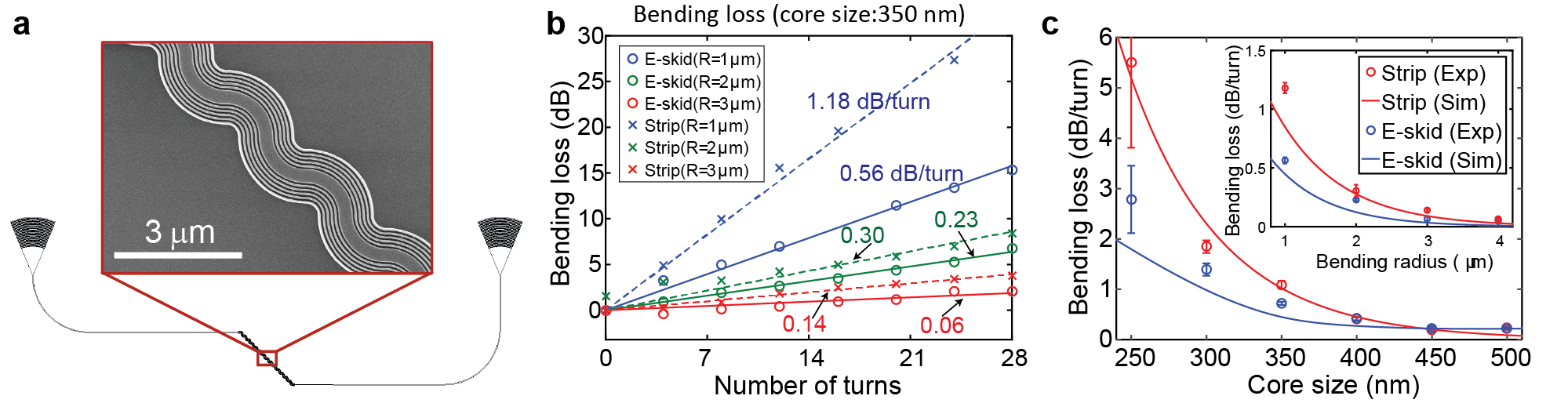
To confirm the effect of the anisotropic metamaterial claddings on the bending loss, we have investigated the bending losses of the e-skid and strip waveguides, both experimentally and numerically Lumerical FDTD Solutions . To characterize the bending losses, we have cascaded bent waveguides sequentially with different numbers of turns (Fig. 6a and Supplementary note 4), then characterized the bending loss per turn by comparing the transmissions. Figures 6b and 6c shows the measured bending losses vs. the core size and the bending radius. In all cases, the bending losses with the e-skid waveguide is lower than that with the strip waveguide, which is due to the reduced skin-depth with the anisotropic metamaterial claddings. Note that if the fabrication advancements on the CMOS platform allowed us to reduce the feature size and approach an ideal anisotropic cladding (), we would achieve further reduction of the bending loss for TE-like modes in e-skid waveguides (See Supplementary note 4 for more details as well as the bending loss calculation for TM-like modes). Our simulations account for all sources of bending loss including radiation and mode-mismatch.
Discussion
In summary, we have introduced a photonic platform which can add the critical but overlooked functionality of controlling evanescent waves to the CMOS foundry. We have shown that high index contrast grating structures in the deep sub-wavelength limit can act as an all-dielectric metamaterial cladding for simultaneously achieving total internal reflection and controlling the skin-depth of evanescent waves. The coupling length is improved more than an order of magnitude and the bending loss is improved three times compared to conventional on-chip waveguides with an average propagation loss of 3.67 dB/cm at telecommunication wavelengths. The decreased photonic skin depth regime has not been realized till date but has been attempted in initial studies Khavasi et al. (2016). This is because anisotropic all-dielectric metamaterial response requires more than one period of the unit cell to control evanescent wave decay Jahani and Jacob (2014, 2015a, 2015b). Although we use Electron Beam Lithography (EBL) as a convenient prototyping technique for the sub-wavelength structures, these devices can in principle be fabricated using deep ultraviolet (DUV) CMOS foundries; specifically, advanced 193 nm immersion lithography technology has been used to fabricate silicon photonic devices with feature sizes down to 50 nm Selvaraja et al. (2014). Our work paves the way for all-dielectric metamaterials to enter the practical realm of CMOS foundry photonics to achieve improved photonic integrated circuits.
Methods
Si/SiO2 multilayers were fabricated using magnetron sputtering and magnetron reactive sputtering, respectively. Silicon and silica were both deposited at a power of 150 W using a pulsed power supply at a frequency of 150 kHz and off time of 0.5 s for silicon and 0.8 s for silica. A special substrate holder was built to hold the prisms during deposition. With the new substrate holder and the large thickness of the prism, the film properties would change as the substrate was much closer to the target, producing films with higher loss. Reducing the deposition power produced lower loss films. A 200 nm thick layer of tungsten was deposited at 300 W, 150 kHz and 0.5 s on top of the multilayer structure at each fill fraction. The prism was illuminated with a 1530 nm narrow line width laser. A broadband linear polarizer placed in the beam path created s and p polarized light. The incident angle was increased in increments of 2∘ from 10∘ to 80∘. A Newport Optics Optical Power Meter calibrated to a wavelength of 1530 nm was then used to measure the reflected power. The two reflections at the prism/air interface in the optical path were accounted for when comparing experiment to EMT simulations.
The on-chip devices for measuring cross-talk in the main text and bending loss in Supplementary Figure 9 were fabricated using a JEOL JBX-6300FS Electron Beam Lithography system Bojko et al. (2011) operated at 100 keV energy, 8 nA beam current, and 500 m exposure field size. A silicon-on-insulator wafer (220 nm thick silicon on 3 m thick silicon dioxide) has been used. A solvent rinse and hot-plate dehydration baked. Then, hydrogen silsesquioxane resist (HSQ, Dow-Corning XP-1541-006) was spin-coated at 4000 rpm, and then hotplate baked at 80 ∘C for 4 minutes. Shape placement by the machine grid, the beam stepping grid, and the spacing between dwell points during the shape writing, were 1 nm, 6 nm, and 6 nm, respectively. An exposure dose of 2800 C/cm2 was used. The resist was developed by immersion in 25% tetramethylammonium hydroxide for 4 minutes, followed by a flowing deionized water rinse for 60 s, an isopropanol rinse for 10 s. Then blown dry with nitrogen. The inductively coupled plasma etching in an Oxford Plasmalab System 100 was used to remove silicon from unexposed areas, with a chlorine gas flow of 20 sccm, ICP power of 800 W, pressure of 12 mT, bias power of 40 W, and a platen temperature of 20 ∘C, resulting in a bias voltage of 185 V. During etching, perfluoropolyether vacuum oil was used to mount chips on a 100 mm silicon carrier wafer. Cladding oxide was deposited using plasma enhanced chemical vapor deposition (PECVD) in an Oxford Plasmalab System 100 with nitrous oxide (N2O) flow of 1000.0 sccm, a silane (SiH4) flow of 13.0 sccm, high-purity nitrogen (N2) flow of 500.0 sccm, high-frequency RF power of 120 W, pressure at 1400 mT, and a platen temperature of 350 ∘C. Chips rest directly on a silicon carrier wafer during deposition and are buffered by silicon pieces on all sides to aid uniformity.
To characterize the on-chip devices, a custom-built automated test setup was used Chrostowski and Hochberg (2015). An Agilent 81635A optical power sensor was used as the output detector and Agilent 81600B tunable laser as the input source. The wavelength was swept in 10 pm steps from 1500 to 1600 nm. To maintain the polarization state of the light, a polarization maintaining fiber was used for coupling the TE polarization into the grating couplers Wang et al. (2014). A polarization maintaining fiber array was used to couple light in/out of the chip.
For the bending loss experiment in the main text, the cross-talk experiment in Supplementary Figure 8, the insertion loss experiments in Supplementary Figure 13, and the propagation loss experiment in Supplementary Figure 14, a standard SOI wafer is used as a substrate with 2 m buried oxide (BOX) and 220 nm top silicon layer. Diluted hydrogen silsesquioxane (HSQ) with methyl isobutyl ketone (MIBK) was spun on the substrate as a negative-tone electron beam resist layer. The resist layer was exposed by a 100 kV electron-beam lithography system, VB6-UHR (Raith), which is capable of 2 nm beam step resolution. After the development of the resist, the top silicon layer was etched by Cl2/O2 based reactive-ion plasma etching tool (Panasonic P610) to transfer the waveguide pattern from the resist to the silicon layer.
Data availability. The data that support the findings of this study are available from the corresponding authors upon request.
Acknowledgements
This work is supported by National Science Foundation (DMR-1654676). M. Qi acknowledges partial in-kind support by the Strategic Priority Fundamental Research Program (category B) from the Chinese Academy of Sciences under grant XDB24020200, and a Key Project in Silicon Photonics from the Shanghai Municipal Government. S. Jahani and Z. Jacob acknowledge the edX UBCx Silicon Photonics Design, Fabrication and Data Analysis course, supported by the Natural Sciences and Engineering Research Council of Canada (NSERC) Silicon Electronic-Photonic Integrated Circuits (SiEPIC) Program. Some of the on-chip devices for measuring the cross-talk were fabricated by Richard Bojko at the University of Washington Washington Nanofabrication Facility. Some of the cross-talk measurements were performed by Zeqin Lu at The University of British Columbia. We acknowledge KLayout and SiEPIC EBeam PDK for the design software.
Author contributions statement
S.J., S.K., J.A., and F.K. designed the experiments. S.K., J.A., J.C.W., A.A.N., K.H. performed the experiments. S.J., S.K., J.A., A.A.N., and P.S. performed the characterizations and measurements. S.J., S.K., and W.D.N. analyzed the data. S.J. and S.K. conducted numerical simulations and prepared the figures. S.J., S.K., and Z.J. wrote the manuscript. All authors discussed the results and commented on the manuscript. Z.J. and M.Q. supervised the project.
Additional information
Competing financial interests: the Authors declare no Competing Financial or Non-Financial Interests.
Supplementary information: controlling evanescent waves using silicon photonic all-dielectric metamaterials for dense integration
Saman Jahani1,2*, Sangsik Kim2,3*, Jonathan Atkinson1, Justin C. Wirth2, Farid Kalhor1,2, Abdullah Al Noman2, Ward D. Newman1,2, Prashant Shekhar1, Kyunghun Han2, Vien Van1, Raymond G. DeCorby1, Lukas Chrostowski4, Minghao Qi2,5, and Zubin Jacob1,2
1 Department of Electrical and Computer Engineering,
University of Alberta, Edmonton, AB T6G 1H9 Canada.
2 School of Electrical and Computer Engineering and Birck Nanotechnology Center,
Purdue University, West Lafayette, IN 47907 USA.
3 Department of Electrical and Computer Engineering,
Texas Tech University, Lubbock, TX 79409 and
4 Department of Electrical and Computer Engineering,
University of British Columbia, Vancouver, BC, V6T 1Z4 Canada.
5 Shanghai Institute of Microsystem and Information Technology,
Chinese Academy of Sciences, Shanghai 200050, China.
 |
SUPPLEMENTRY NOTE 1 Relaxed total internal reflection
Supplementary Figure 7 displays the field profile for p-polarized plane-wave propagation through an Si/SiO2 multilayer sandwiched between two Si half spaces. The incident angle is (top) and (bottom). In both cases, nm and , and light is incident from the left side at nm. The gray and yellow regions represent Si and SiO2 layers, respectively. The critical angle of the effective medium is based on relaxed-TIR theory. It is seen that above the critical angle, the electromagnetic wave is totally reflected back to the left side and forms a standing wave on the left side but decays inside the multilayer and negligible power is transmitted to the right half space. However, when the incident angle is below the critical angle, most of the power is transmitted through the multilayer because the total thickness of the slab is thin in comparison with the wavelength.
SUPPLEMENTRY NOTE 2 Effect of periodicity and disorder on e-skid waveguides
Although practical metamaterial structures for realization of strong effective anisotropy are usually periodic, the effective macroscopic electromagnetic response of metamaterials does not stem from the periodicity (or unit-cell size). As long as the periodicity of the metamaterial building blocks is deeply subwavelength, the change in the periodicity does not change the electromagnetic response of metamaterials. Indeed, according to the effective medium theory (EMT), which has been explained in the main text, the effective constitutive parameters of multilayer metamaterials depend on the permittivity of the building blocks and their filling fraction, not the periodicity of the multilayer.
To demonstrate the effect of periodicity on the performance of e-skid waveguides, we analyzed 1D e-skid waveguides with multilayer claddings of the same total size, but different periodicities as illustrated in Supplementary Fig. 8. We also analyzed a case where the multilayer is not periodic. We can see that since the effective permittivity for all three cases is the same, the performance of the waveguides are almost identical. This demonstrates that the light confinement mechanism in e-skid waveguides and photonic crystal waveguides are fundamentally different. In photonic crystal waveguides, the periodicity is a requirement and a change in periodicity strongly affects the performance of the waveguide.
We have also studied the effect of periodicity on the modal effective index () of TE-like and TM-like modes of a single on-chip e-skid waveguide as a function of core size at =1550 nm. Supplementary Figure 9 shows that EMT is an extremely accurate approximation to homogenize the cladding when the unit cell size is considerably smaller than the operating wavelength. The effect of the unit-cell size is more obvious on the effective index of the TE-like mode because the field intensity is higher in the cladding region for these modes.
 |
 |
SUPPLEMENTRY NOTE 3 Cross-talk
In the main text, we have reported the coupled power at a single wavelength. However, the coupling between two waveguides is a function of frequency in general. Supplementary Figure 10 displays the spectral response of strip and e-skid couplers. Since multilayer metamaterials are non-resonant broadband structures, multilayers show strong anisotropy for a wide range of wavelengths as long as the period is considerably smaller than the wavelength. Hence, as shown in Supplementary Fig. 10, the multilayer cladding causes the cross-talk to decrease for a broad range of frequencies.
An important challenge of alternative waveguides is mode conversion efficiency from the grating coupler to the waveguide. The comparison of the output level of the through waveguide shows that the coupling efficiency from the grating coupler to the e-skid waveguides is very close to the coupling efficiency in strip waveguides. Moreover, as we explain in Supplementary note 5, the mode conversion efficiency from a strip waveguide to an e-skid waveguide with the same core size is above 98%. This means that e-skid waveguides can easily be integrated to the silicon photonics chip. Supplementary Figure 11 illustrates the normalized coupling length versus the center-to-center separation for coupled e-skid and strip waveguides. For a compact photonic circuit, minimum separation with maximum decoupling between adjacent waveguides are required Dai et al. (2007). However, as it is seen in Supplementary Fig. 11, the coupling length exponentially decreases as the separation is reduced. This trade-off limits the integration density of photonic circuits. Due to the reduced skin-depth in e-skid waveguides, we can reduce the decoupled separation further and increase the integration density of photonic integrated circuits. We should emphasize that the decoupled separation in slot waveguides and photonic crystal waveguides are even more than that in strip waveguides Dai et al. (2007).
We also contrast the effect of anisotropy on TE-like and TM-like modes of on-chip e-skid waveguides. Supplementary Figure 12 shows the coupling length for TE-like and TM-like modes versus while is fixed in the cladding. As the anisotropy increases, we can reduce the skin-depth in the cladding for TE-like mode. Thus, the coupling length between the two coupled waveguides is strongly enhanced because the overlap between evanescent waves of adjacent waveguides is suppressed. On the other hand, since the electric field in the direction is negligible for TM-like modes, these modes cannot feel the anisotropy of the cladding. Hence, the anisotropic cladding cannot help to control the momentum of evanescent waves for TM-like modes.
To control the evanescent waves of TM-like modes, the cladding must be anisotropic in the plane and it must be added beneath or above the waveguide core. Supplementary Figure 13a (inset) illustrates a simplified structure to control the skin-depth of TM-like modes. We keep the permittivity in the direction fixed, but we change it in the direction to control the anisotropy. As we increase the permittivity in the direction, the optical mode is confined inside the core and the overlap between the evanescent tales is reduced. Hence, as shown in Supplementary Fig. 13a, the coupling length increases. Supplementary Figure 13b displays a practical implementation of the anisotropic cladding for the TM-like modes composed of Si/SiO2 multilayer claddings. In this case, nm and the silicon filling fraction is . Supplementary Figure 13c and 13d show the normalized electric field profile of the even mode of the coupled strip and e-skid waveguides, respectively. It is seen that the skin-depth of the evanescent waves in e-skid waveguides is reduced, and as a result, the coupling length has been increased from for strip waveguides case to for e-skid waveguides case. Note that if we add the multilayer on top of the waveguide core as well, more confinement is achievable and the cross-talk can be reduced further.
 |
 |
 |
 |

 |
 |
 |
 |
 |
Cross-talk in E-skid Waveguides Without an Upper Cladding
In an e-skid waveguide, the waveguide cross-talk can be reduced further by increasing the anisotropy of the metamaterial. Supplementary Figure 14a shows the schematic layout to measure the cross-talk between coupled e-skid waveguides, and Supplementary Fig. 14b shows an SEM image of coupled e-skid waveguides. The parameters for the e-skid waveguide are set to nm, nm, , and ; this sets the separation distance between the two waveguides (edge-to-edge) to be nm, which is less than a free space wavelength ( nm). In this case, there is no upper SiO2 cladding and the cross-section is similar to that in Fig. 3c of the main manuscript (Si/air multilayers). This leads to a higher anisotropy in metamaterials and reduces the skin-depth of the guided mode compared to the case of Si/SiO2 multilayers. To evaluate the waveguide cross-talk, as in the main text, we have characterized the coupling length by measuring the output power ratio () for different lengths () of devices. Red and blue circles in Supplementary Figs. 14c-14e are the measured output power ratio for e-skid and strip waveguides, respectively, and dashed lines are their respective fitting curves with . Supplementary Figures 14c-14e are with different core widths of 350, 400, and 450 nm, respectively. Supplementary Figure 14f summarizes the normalized coupling lengths () that are characterized through Supplementary Figs. 14c-14e: e-skid (red circles) and strip (blue circles) waveguides. The solid lines are their respective simulation results that match well with the experimental measurements. Notice that, in every case, the coupling length of an e-skid waveguide is much longer than that of a strip waveguide. The maximum coupling length of more than 3 cm is achieved ( nm), and, when is 400 or 450 nm, the coupling length for an e-skid waveguide is about 30 times longer in comparison with strip waveguide.
 |
SUPPLEMENTRY NOTE 4 Bending loss
We have also simulated CST Microwave Studio and measured the bending loss when the waveguides are coated by an SiO2 upper cladding (Supplementary Fig. 15). An oxide cladding is usually used to protect the device and to integrate it with electronic interconnects Chrostowski and Hochberg (2015). In this experiment, the input power is divided into two paths with equal lengths. It is seen that the bending loss is considerably reduced due to the metamaterial cladding even when the core size is large.
In the main text, we have presented the magnetic field of curved strip waveguides and e-skid waveguides using a transformation optics approach to demonstrate the effect of skin-depth on the bending loss. However, for accurate calculation of bending loss, 3D full-wave simulations are required. Supplementary Figure 16 shows the top view of the simulated CST Microwave Studio magnetic field profile of TE-like mode for curved strip and e-skid waveguides. It is seen that for all-cases the skin-depth extends on the right side and is compressed on the left side in agreement with the transformation optics calculations. The performance of e-skid waveguides improves if we approach the effective medium theory limit () (Supplementary Fig. 16). As we mentioned earlier, the TM-like mode of on-chip waveguides does not feel the anisotropy of the cladding because the electric field in the direction is negligible. Hence, the confinement of the TM-like mode in e-skid cladding is the same as that in an isotropic cladding as shown in Supplementary Fig. 17.
We compare the bending loss for both TE-like and TM-like modes of e-skid and strip waveguides in Supplementary Fig. 18. As we mentioned in the main text, the additional degree of freedom in total internal reflection can be used to control evanescent waves of p-polarized (TE-like) modes. Hence, the anisotropic cladding helps to reduce the bending loss of the TE-like mode in e-skid waveguides in comparison with strip waveguides. However, this degree of freedom does not exist for s polarized (TM-like) modes. Since the effective permittivity of the cladding for the TM-like mode is larger than the permittivity of SiO2, the evanescent waves decay slower for TM-like modes in e-skid waveguides. Thus, the skin-depth extends more and more power is radiated at sharp bends in comparison with strip waveguides.
SUPPLEMENTRY NOTE 5 Mode conversion efficiency
The mode conversion efficiency between the e-skid waveguide and the strip waveguide are also investigated. For the mode conversion efficiency, we use a racetrack resonator (Supplementary Fig. 19) to characterize the insertion loss efficiency Han et al. (2016). Supplementary Figure 19c shows the normalized transmission spectra for the e-skid (red) and strip (blue) waveguides. The resonances are slightly shifted with metamaterials due to the different propagation phase in the e-skid waveguide (see Fig. 3 in the main text), but the extinction ratios are almost similar suggesting a similar cavity loss. Supplementary Figures 19d and 19e are the fitted resonances for the strip and e-skid waveguides, respectively, and the intrinsic quality factors are 26,518 and 24,535, which correspond to the round-trip losses of 0.6893 dB/round and 0.7466 dB/round, respectively Xiao et al. (2007). Since we have four interfaces for the mode conversion, a rough estimation of the mode conversion loss is about 0.0143 dB/facet, which corresponds to a mode conversion efficiency of 99.6%. The mode conversion efficiencies (CEs) with other resonances are also characterized and plotted in Supplementary Fig. 19c. This high mode conversion efficiency between the strip waveguide and the e-skid waveguide in TE-like modes indicates a low insertion loss, and suggests a high compatibility with the previously used PIC devices.
SUPPLEMENTRY NOTE 6 Propagation loss
To characterize the propagation losses in the e-skid and the strip waveguides, we have fabricated two sets of waveguides (e-skid and strip waveguides) with different lengths of the straight section. The waveguide parameters are set to nm, nm, nm, and ; then the lengths of the straight section of the e-skid and strip waveguides are varied from 0 to 1.8 mm. Supplementary Figure 20 shows the measured transmission powers of e-skid (blue circles) and strip (red circles) waveguides at nm, for different device lengths. Solid lines in each figure are the linear fitting curves that give the propagation losses of 2.65 dB/cm and 3.43 dB/cm to strip and e-skid waveguides, respectively. The propagation losses for strip and e-skid waveguides at different wavelengths have also been characterized. The average losses for strip and e-skid waveguides for wavelengths between 1540 nm to 1560 nm are 1.84 dB/cm and 3.67 dB/cm, respectively, with a standard deviation of 1.4 dB/cm and 1.0 dB/cm, respectively. This propagation loss of the e-skid waveguide is reasonable for compact devices, especially given that the cross-talks and bending losses are improved significantly (see Table I in the main text for comparison with other techniques).
References
- Jalali and Fathpour (2006) B. Jalali and S. Fathpour, Journal of Lightwave Technology 24, 4600 (2006).
- Bogaerts et al. (2005) W. Bogaerts, R. Baets, P. Dumon, V. Wiaux, S. Beckx, D. Taillaert, B. Luyssaert, J. V. Campenhout, P. Bienstman, and D. V. Thourhout, Journal of Lightwave Technology 23, 401 (2005).
- Nagarajan et al. (2005) R. Nagarajan, C. H. Joyner, R. P. Schneider, J. S. Bostak, T. Butrie, A. G. Dentai, V. G. Dominic, P. W. Evans, M. Kato, M. Kauffman, D. J. H. Lambert, S. K. Mathis, A. Mathur, R. H. Miles, M. L. Mitchell, M. J. Missey, S. Murthy, A. C. Nilsson, F. H. Peters, S. C. Pennypacker, J. L. Pleumeekers, R. A. Salvatore, R. K. Schlenker, R. B. Taylor, H.-S. Tsai, M. F. V. Leeuwen, J. Webjorn, M. Ziari, D. Perkins, J. Singh, S. G. Grubb, M. S. Reffle, D. G. Mehuys, F. A. Kish, and D. F. Welch, IEEE Journal of Selected Topics in Quantum Electronics 11, 50 (2005).
- Soref (2006) R. Soref, IEEE Journal of Selected Topics in Quantum Electronics 12, 1678 (2006).
- Kim et al. (2017) S. Kim, K. Han, C. Wang, J. A. Jaramillo-Villegas, X. Xue, C. Bao, Y. Xuan, D. E. Leaird, A. M. Weiner, and M. Qi, Nature Communications 8, 372 (2017).
- Chrostowski and Hochberg (2015) L. Chrostowski and M. Hochberg, Silicon Photonics Design: From Devices to Systems (Cambridge University Press, 2015).
- Dai et al. (2012) D. Dai, J. Bauters, and J. E. Bowers, Light: Science & Applications 1, e1 (2012).
- Heck et al. (2013) M. J. R. Heck, J. F. Bauters, M. L. Davenport, J. K. Doylend, S. Jain, G. Kurczveil, S. Srinivasan, Y. Tang, and J. E. Bowers, IEEE Journal of Selected Topics in Quantum Electronics 19, 6100117 (2013).
- Luo et al. (2014) L.-W. Luo, N. Ophir, C. P. Chen, L. H. Gabrielli, C. B. Poitras, K. Bergmen, and M. Lipson, Nature Communications 5, 3069 (2014).
- Momeni et al. (2009) B. Momeni, S. Yegnanarayanan, M. Soltani, A. A. Eftekhar, E. S. Hosseini, and A. Adibi, Journal of Nanophotonics 3, 031001 (2009).
- Shen et al. (2017) Y. Shen, N. C. Harris, S. Skirlo, M. Prabhu, T. Baehr-Jones, M. Hochberg, X. Sun, S. Zhao, H. Larochelle, D. Englund, and M. Soljačić, Nature Photonics 11, 441 (2017).
- Dionne et al. (2006) J. A. Dionne, L. A. Sweatlock, H. A. Atwater, and A. Polman, Physical Review B 73, 035407 (2006).
- Oulton et al. (2008) R. F. Oulton, V. J. Sorger, D. A. Genov, D. F. P. Pile, and X. Zhang, Nature Photonics 2, 496 (2008).
- Gramotnev and Bozhevolnyi (2010) D. K. Gramotnev and S. I. Bozhevolnyi, Nature Photonics 4, 83 (2010).
- Alù and Engheta (2009) A. Alù and N. Engheta, Physical Review Letters 103, 143902 (2009).
- Kim and Qi (2015a) S. Kim and M. Qi, Scientific Reports 5, 18378 (2015a).
- Kim and Qi (2015b) S. Kim and M. Qi, Optics Express 23, 9968 (2015b).
- Raza et al. (2014) S. Raza, N. Stenger, A. Pors, T. Holmgaard, S. Kadkhodazadeh, J. B. Wagner, K. Pedersen, M. Wubs, S. I. Bozhevolnyi, and N. A. Mortensen, Nature Communications 5, 4125 (2014).
- Kinsey et al. (2015) N. Kinsey, M. Ferrera, V. M. Shalaev, and A. Boltasseva, Journal of the Optical Society of America B 32, 121 (2015).
- Khurgin (2015) J. B. Khurgin, Nature Nanotechnology 10, 2 (2015).
- Khurgin (2017) J. B. Khurgin, Phil. Trans. R. Soc. A 375, 20160068 (2017).
- Jahani and Jacob (2016) S. Jahani and Z. Jacob, Nature Nanotechnology 11, 23 (2016).
- Priolo et al. (2014) F. Priolo, T. Gregorkiewicz, M. Galli, and T. F. Krauss, Nature Nanotechnology 9, 19 (2014).
- Kuznetsov et al. (2016) A. I. Kuznetsov, A. E. Miroshnichenko, M. L. Brongersma, Y. S. Kivshar, and B. Luk’yanchuk, Science 354, aag2472 (2016).
- Staude and Schilling (2017) I. Staude and J. Schilling, Nature Photonics 11, 274 (2017).
- Chang-Hasnain and Yang (2012) C. J. Chang-Hasnain and W. Yang, Advances in Optics and Photonics 4, 379 (2012).
- Krasnok et al. (2012) A. E. Krasnok, A. E. Miroshnichenko, P. A. Belov, and Y. S. Kivshar, Optics Express 20, 20599 (2012).
- Baranov et al. (2017) D. G. Baranov, D. A. Zuev, S. I. Lepeshov, O. V. Kotov, A. E. Krasnok, A. B. Evlyukhin, and B. N. Chichkov, Optica 4, 814 (2017).
- Liu et al. (2016) W. Liu, A. E. Miroshnichenko, and Y. S. Kivshar, Physical Review B 94, 195436 (2016).
- Arbabi et al. (2015) A. Arbabi, Y. Horie, M. Bagheri, and A. Faraon, Nature Nanotechnology 10, 937 (2015).
- Arbabi et al. (2016) E. Arbabi, A. Arbabi, S. M. Kamali, Y. Horie, and A. Faraon, Optica 3, 628 (2016).
- Khorasaninejad et al. (2016) M. Khorasaninejad, W. T. Chen, R. C. Devlin, J. Oh, A. Y. Zhu, and F. Capasso, Science 352, 1190 (2016).
- Shen et al. (2015a) B. Shen, P. Wang, R. Polson, and R. Menon, Nature Photonics 9, 378 (2015a).
- Piggott et al. (2015) A. Y. Piggott, J. Lu, K. G. Lagoudakis, J. Petykiewicz, T. M. Babinec, and J. Vuckovic, Nature Photonics 9, 374 (2015).
- Hafezi et al. (2013) M. Hafezi, S. Mittal, J. Fan, A. Migdall, and J. M. Taylor, Nature Photonics 7, 1001 (2013).
- Slobozhanyuk et al. (2016) A. Slobozhanyuk, S. H. Mousavi, X. Ni, D. Smirnova, Y. S. Kivshar, and A. B. Khanikaev, Nature Photonics (2016).
- Jahani and Jacob (2014) S. Jahani and Z. Jacob, Optica 1, 96 (2014).
- Joannopoulos et al. (2008) J. D. Joannopoulos, S. G. Johnson, J. N. Winn, and R. D. Meade, Photonic Crystals: Molding the Flow of Light, Second Edition (Princeton University Press, 2008).
- Benisty et al. (1999) H. Benisty, C. Weisbuch, D. Labilloy, M. Rattier, C. J. M. Smith, T. F. Krauss, R. M. d. l. Rue, R. Houdre, U. Oesterle, C. Jouanin, and D. Cassagne, Journal of Lightwave Technology 17, 2063 (1999).
- Hsu et al. (2013) C. W. Hsu, B. Zhen, J. Lee, S.-L. Chua, S. G. Johnson, J. D. Joannopoulos, and M. Soljačić, Nature 499, 188 (2013).
- Mekis et al. (1996) A. Mekis, J. C. Chen, I. Kurland, S. Fan, P. R. Villeneuve, and J. D. Joannopoulos, Physical Review Letters 77, 3787 (1996).
- Dai et al. (2007) D. Dai, Y. Shi, and S. He, Applied Optics 46, 1126 (2007).
- Almeida et al. (2004) V. R. Almeida, Q. Xu, C. A. Barrios, and M. Lipson, Optics Letters 29, 1209 (2004).
- Song et al. (2015) W. Song, R. Gatdula, S. Abbaslou, M. Lu, A. Stein, W. Y.-C. Lai, J. Provine, R. F. W. Pease, D. N. Christodoulides, and W. Jiang, Nature Communications 6, 7027 (2015).
- Mrejen et al. (2015) M. Mrejen, H. Suchowski, T. Hatakeyama, C. Wu, L. Feng, K. O’Brien, Y. Wang, and X. Zhang, Nature Communications 6, 7565 (2015).
- Gabrielli et al. (2012) L. H. Gabrielli, D. Liu, S. G. Johnson, and M. Lipson, Nature Communications 3, 1217 (2012).
- Shen et al. (2015b) B. Shen, R. Polson, and R. Menon, Optics Letters 40, 5750 (2015b).
- Shen et al. (2016) B. Shen, R. Polson, and R. Menon, Nature Communications 7, 13126 (2016).
- Jahani and Jacob (2015a) S. Jahani and Z. Jacob, Journal of the Optical Society of America B 32, 1346 (2015a).
- Bock et al. (2010) P. J. Bock, P. Cheben, J. H. Schmid, J. Lapointe, A. Delâge, S. Janz, G. C. Aers, D.-X. Xu, A. Densmore, and T. J. Hall, Optics Express 18, 20251 (2010).
- Halir et al. (2015) R. Halir, P. J. Bock, P. Cheben, A. Ortega-Moñux, C. Alonso-Ramos, J. H. Schmid, J. Lapointe, D.-X. Xu, J. G. Wangüemert-Pérez, . Molina-Fernández, and S. Janz, Laser & Photonics Reviews 9, 25 (2015).
- Yang et al. (2008) S.-H. Yang, M. L. Cooper, P. R. Bandaru, and S. Mookherjea, Optics Express 16, 8306 (2008).
- Levy et al. (2005) U. Levy, M. Nezhad, H.-C. Kim, C.-H. Tsai, L. Pang, and Y. Fainman, Journal of the Optical Society of America A 22, 724 (2005).
- Murray et al. (2015) K. Murray, Z. Lu, H. Jayatilleka, and L. Chrostowski, Optics Express 23, 19575 (2015).
- Zhang et al. (2015) F. Zhang, H. Yun, V. Donzella, Z. Lu, Y. Wang, Z. Chen, L. Chrostowski, and N. A. Jaeger, in CLEO: Science and Innovations (Optical Society of America, 2015) pp. SM1I–7.
- Jahani and Jacob (2015b) S. Jahani and Z. Jacob, IEEE Photonics Journal 7, 1 (2015b).
- Milton (2002) G. W. Milton, The Theory of Composites, 1st ed. (Cambridge University Press, 2002).
- Herzig Sheinfux et al. (2014) H. Herzig Sheinfux, I. Kaminer, Y. Plotnik, G. Bartal, and M. Segev, Physical Review Letters 113, 243901 (2014).
- Halir et al. (2016) R. Halir, P. Cheben, J. M. Luque-González, J. D. Sarmiento-Merenguel, J. H. Schmid, G. Wangüemert-Pérez, D.-X. Xu, S. Wang, A. Ortega-Moñux, and . Molina-Fernández, Laser & Photonics Reviews 10, 1039 (2016).
- Sayem et al. (2016) A. A. Sayem, M. R. C. Mahdy, and M. S. Rahman, Journal of Optics 18, 015101 (2016).
- Gomis-Bresco et al. (2017) J. Gomis-Bresco, D. Artigas, and L. Torner, Nature Photonics 11, 232 (2017).
- Li et al. (2017) H. Li, S. Atakaramians, R. Lwin, X. Tang, Z. Yu, A. Argyros, and B. T. Kuhlmey, Optica 3, 941 (2017).
- Dyakonov (1988) M. I. Dyakonov, Sov. Phys. JETP 67, 714 (1988).
- Takayama et al. (2009) O. Takayama, L. Crasovan, D. Artigas, and L. Torner, Physical Review Letters 102, 043903 (2009).
- Takayama et al. (2014) O. Takayama, D. Artigas, and L. Torner, Nature Nanotechnology 9, 419 (2014).
- Polo and Lakhtakia (2011) J. Polo and A. Lakhtakia, Laser & Photonics Reviews 5, 234 (2011).
- Talebi et al. (2016) N. Talebi, C. Ozsoy-Keskinbora, H. M. Benia, K. Kern, C. T. Koch, and P. A. van Aken, ACS Nano 10, 6988 (2016).
- Boroojerdi et al. (2016) M. T. Boroojerdi, M. Ménard, and A. G. Kirk, Optics Express 24, 22865 (2016).
- Fiore et al. (1998) A. Fiore, V. Berger, E. Rosencher, P. Bravetti, and J. Nagle, Nature 391, 463 (1998).
- Wang et al. (2014) Y. Wang, X. Wang, J. Flueckiger, H. Yun, W. Shi, R. Bojko, N. A. F. Jaeger, and L. Chrostowski, Optics Express 22, 20652 (2014).
- (71) CST Microwave Studio, http://www.cst.com .
- Heiblum and Harris (1975) M. Heiblum and J. Harris, IEEE Journal of Quantum Electronics 11, 75 (1975).
- Vlasov and McNab (2004) Y. A. Vlasov and S. J. McNab, Optics Express 12, 1622 (2004).
- Marcatili (1969) E. A. J. Marcatili, The Bell System Technical Journal 48, 2103 (1969).
- Han et al. (2013) Z. Han, P. Zhang, and S. I. Bozhevolnyi, Optics Letters 38, 1778 (2013).
- (76) Lumerical FDTD Solutions, http://www.lumerical.com .
- Khavasi et al. (2016) A. Khavasi, L. Chrostowski, Z. Lu, and R. Bojko, IEEE Photonics Technology Letters 28, 2787 (2016).
- Selvaraja et al. (2014) S. K. Selvaraja, G. Winroth, S. Locorotondo, G. Murdoch, A. Milenin, C. Delvaux, P. Ong, S. Pathak, W. Xie, G. Sterckx, G. Lepage, D. V. Thourhout, W. Bogaerts, J. V. Campenhout, and P. Absil, Proceeding of SPIE 9052, 90520F (2014).
- Bojko et al. (2011) R. J. Bojko, J. Li, L. He, T. Baehr-Jones, M. Hochberg, and Y. Aida, Journal of Vacuum Science & Technology B 29, 06F309 (2011).
- Han et al. (2016) K. Han, S. Kim, J. Wirth, M. Teng, Y. Xuan, B. Niu, and M. Qi, Optics Express 24, 6532 (2016).
- Xiao et al. (2007) S. Xiao, M. H. Khan, H. Shen, and M. Qi, Optics Express 15, 10553 (2007).