Topological suppression of magnetoconductance oscillations in NS junctions
Abstract
We show that the magnetoconductance oscillations of laterally-confined 2D NS junctions are completely suppressed when the superconductor side enters a topological phase. This suppression can be attributed to the modification of the vortex structure of local currents at the junction caused by the topological transition of the superconductor. The two regimes (with and without oscillations) could be seen in a semiconductor 2D junction with a cleaved-edge geometry, one of the junction arms having proximitized superconductivity. We predict similar oscillations and suppression as a function of the Rashba coupling. The oscillation suppression is robust against differences in chemical potential and phases of lateral superconductors.
pacs:
73.63.Nm,74.45.+cI Introduction
Magnetoconductance oscillations are a central topic of the field of quantum transport in nanostructures. Famous examples are the celebrated Aharonov-Bohm oscillations in a quantum ring and the Shubnikov-deHass oscillations in the quantum Hall effect Ihn (2010). In a general sense, the accumulation of complex phases (angles) in the wave function during orbital motion in a perpendicular magnetic field is the basic cause behind the magnetoconductance oscillations. In presence of a superconductivity pairing gap, transport can be described as the propagation of electron and hole quasiparticles, with Andreev processes allowing the transformation of one type into the other. Andreev reflections in a normal-superconductor (NS) junction are affected by a magnetic field acting on the normal side, the field thus modifying the magnetoconductance of the junction.
The interplay of Andreev reflection and magnetic orbital effects has received a long lasting attention Beenakker (1992); Takagaki (1998); Asano (2000); Hoppe et al. (2000); Giazotto et al. (2005); Eroms et al. (2005); Chtchelkatchev and Burmistrov (2007); Rakyta et al. (2007); Khaymovich et al. (2010); Carmier (2013). In particular, Takagaki Takagaki (1998) studied the magnetoconductance of a 2D NS junction, laterally confined to a width and with the N terminal being a semiconductor. As the magnetic field is increased the magnetoconductance tends to decrease in a stepwise manner due to the depopulation of the active Landau bands of the semiconductor. It was predicted, however, that for high enough fields conspicuous magnetoconductance oscillations superimposed to the general stepwise reduction would be present. Maxima are related to (electron-hole) Andreev reflection while minima are due to enhanced normal (electron-electron) reflection. Andreev reflection suppression or enhancement appears because of the spatial separation between the electron and hole edge states, each one attached to a different edge of the N lead. In presence of orbital magnetic effects the only way the two edge channels can be connected is through multiple alternating electron-hole and hole-electron reflections at the transverse boundary of the 2D junction. Therefore the resulting conductance depends on the spatial structure of these reflections with respect to the transverse boundary of the junction. This scenario of magnetoconductance oscillations has been discussed in detail in Refs. Takagaki (1998); Takagaki and Ploog (2000); Asano (2000); Hoppe et al. (2000); Hsue et al. (2004); Giazotto et al. (2005); Eroms et al. (2005); Batov et al. (2007); Chtchelkatchev and Burmistrov (2007); Rakyta et al. (2007); Sun (2008); Khaymovich et al. (2010); Carmier (2013) and it has been experimentally confirmed in Ref. Eroms et al. (2005).
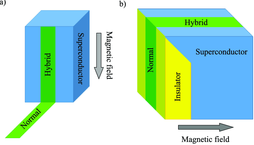
In this work we investigate the fate of Takagaki oscillations when the trivial superconductor lead is replaced by a topological superconductor lead. We consider a 2D junction of semiconductor wires with effective topological superconductivity in one of the junction sides induced by proximity with an -wave superconductor. It has been much studied recently how the resulting hybrid semiconductor-superconductor system can be driven into a topological phase by the combined action of a parallel magnetic field and Rashba spin-orbit interaction Fu and Kane (2008); Oreg et al. (2010); Lutchyn et al. (2010). In hybrid nanowires the characteristic of the topological phase is the emergence of zero-energy Majorana modes attached to possible potential barriers or wire ends Alicea (2012); Leijnse and Flensberg (2012); Beenakker (2013); Franz (2013); Stanescu and Tewari (2013). In this work, we provide evidence that in nanowire junctions the nature of the Andreev reflections changes from the trivial to the topological phase such that magnetoconductance oscillations are completely suppressed in the topological phase. The abrupt magnetoconductance change of behavior across the phase transition is thus another clear signal of the topological superconductivity.
The system we have in mind, sketched in Fig. 1, is a 2D semiconductor wire in a cleaved-edge-like geometry Pfeiffer et al. (1990), with one of the two arms proximitized with a standard -wave superconductor. The magnetic field is such that it is perpendicular and parallel to the normal and proximitized arms, respectively. This way we may simultaneously achieve with a uniform field the required quantum Hall behavior on the N arm and the possibility to induce the topological transition on the hybrid S (proximitized) arm. The cleaved-edge device suggested by Fig. 1 assumes a uniform magnetic field, a realistic approximation in view of the small size of the nanostructure. In principle, non uniform fields could also be created by attaching micromagnets Kjaergaard et al. (2012), but this would possibly be a technically more involved alternative. It should also be stressed that our simplified model only considers the different relative orientations of the magnetic field with respect to the quasiparticle motions, while other effects of the cleavage such as confinement inhomogeneities affecting the motion at the bending are disregarded in a first approximation Londergan et al. (1999).
The work is organized as follows. Section II gives the details of the theoretical model and formalism. In a first stage (Sec. III) the analysis of results is performed assuming the field can be tuned independently in both arms of the junction. This allows a more clear understanding of the physical behavior. The uniform (homogenous) field is then considered in Sec. IV for varying wire widths and Rashba strengths. The robustness of the oscillation suppression for finite biases and considering lateral superconductors of different pairing-gap phases is discussed in Sec. V. Finally, Sec. VI summarizes the conclusions of the work.
II Theoretical model and formalism
We consider nanowires containing all the ingredients to create topological phases and magnetoconductance oscillations. Hybrid nanowires that combine s-wave superconductivity, Rashba interaction, and an external magnetic field in a parallel orientation are known to sustain a topological phase if a critical magnetic field is exceeded Oreg et al. (2010). s-wave hybrid superconductivity is achieved by proximity coupling a semiconductor nanowire with a superconductor while Rashba interaction is a property of the semiconductor nanostructure due to the confinement asymmetry of the nanowire. On the other hand, for magnetoconductance oscillations we need a two-dimensional NS junction with orbital effects in the normal side but not in the superconductor side. This condition is automatically met with true metallic superconductors that do not allow the penetration of magnetic fields to its interior. However, with hybrid nanowires superconductivity is obtained by proximity and a more clever arrangement is needed in order to avoid orbital effects in the gapped region of the hybrid superconducting section, such as in Fig. 1.
II.1 The model
A 2D junction, with and the longitudinal (parallel to transport) and transverse coordinates, respectively, is described by the following Bogoliubov-de Gennes Hamiltonian
| (1) |
where contains the kinetic and confinement potential terms
| (2) |
is the Zeeman term,
| (3) |
is the Rashba spin-orbit term,
| (4) |
and, finally, is the superconductor pairing term
| (5) |
The potential models the transversal confinement, with zero value inside the nanowire and infinite outside. In the Zeeman term, gives the orientation of the field, along and for the N and S sides, respectively. The intensities of Zeeman, Rashba and pairing interactions are given by and they may take different constant values in the N and S sides, i.e., and . Orbital magnetic effects are included for perpendicular fields through the substitution as, e.g., in Ref. Osca and Serra (2015), with the magnetic length defined by the perpendicular component of the field as . The Zeeman parameter is related to the modulus of the magnetic field as , with the effective gyromagnetic factor and the Bohr magneton.
We shall obviously have , i.e., no pairing gap in the normal side, and the model also assumes a priori that the two Zeeman intensities and can be varied independently. The latter is only for discussion purposes since a more realistic situation with a uniform field requires (Sec. IV). Also, different Rashba intensities (, ) represent a modification of the vertical asymmetry, e.g., with a gate, of one of the junction sides with respect to the other.
II.2 Resolution method
For a given energy we study the solutions of the equation
| (6) |
where are the spin and isospin (electron-hole) discrete variables. The solution is obtained by means of the numerical method presented in Osca and Serra (2016). The algorithm is based on the quantum-transmitting-boundary method and, in essence, provides a way of matching two different sets of asymptotic solutions characterized as superpositions of complex- plane waves. Advantages of this approach are the high spatial resolution and the inclusion of large numbers of evanescent modes without requiring large 2D grids, i.e, without exceedingly large computational costs.
In the leads, at both sides of the junction, the wave function can be expressed as a superposition of plane waves, where the wavenumber may be real or complex and is a characteristic of the fully translationally invariant wire Serra (2013). For each lead, labeled as (contact) the wavefunction thus reads
| (7) |
where labels the input/output condition of the mode and the mode number. The wavenumbers and the transversal components are obtained solving a transformed version of the BdG equation for the contacts, recast as a non-Hermitian eigenvalue problem for the wavenumbers Osca and Serra (2016). It is assumed that a large set of them is known. The coefficients , the channel amplitudes, are obtained from the matching equations. Note that the energy is used here as a parameter that is fixed selecting the proper input channel. Finally, the conductance is calculated from the wavefunction as
| (8) |
where
| (9) | |||||
| (10) |
are the normal (electron-electron) and Andreev (electron-hole) reflection probabilities. Note that is the spinor amplitude in a particular electron () or hole () channel with spin () and corresponding to output towards the N lead.
III Independently tunable fields
The results discussed below are given in the same unit system of Ref. Osca and Serra (2015), characterized by a length unit and a corresponding energy unit . A natural choice is , the transverse width of the 2D stripe although below we will also use in some specific cases different values for and . With nm and , typical with InAs, it is meV. From , with the Bohr magneton and (gyromagnetic factor), the magnetic field modulus corresponding to a given is .
III.1 Conductance in trivial and topological phases
Firstly, we study the magnetoconductance of the junction model of Sec. II assuming that the magnetic field in the two junction sides (the two arms of the cleaved-edge nanowire) can be tuned independently. Although this is not very realistic, it is a good starting point from a theoretical point of view as it allows controlling the topological and trivial phases of the (hybrid) superconductor without changing the parameters for the normal side. This way, any difference between the two situations can be ascribed to the superconductor phase condition.
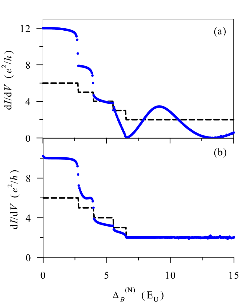
Figures 2a and 2b show the magnetoconductance as a function of the magnetic field on the normal side of the junction , while the superconductor side of the junctions remains under a constant field . The figure also shows the evolution of the number of propagating modes in the normal side (dashed line). Note that, this number decreases with the magnetic field in a stepwise manner, with steps of one unit. This behavior is due to our normal contact including a non zero Zeeman term (cf. Ref. Takagaki (1998)). We consider a nanowire made of an homogeneous material, hence with a constant Rashba term throughout. Together, Rashba and Zeeman terms split and mix the spin degrees of freedom in a way that full pure Andreev reflection is not achieved for low magnetic fields, but there is some normal reflection too. As a consequence, the conductance in this limit is less than two times the number of active modes. Full Andreev reflection at vanishing fields is recovered when disregarding the Zeeman and Rashba terms (but maintaining the orbital effects).
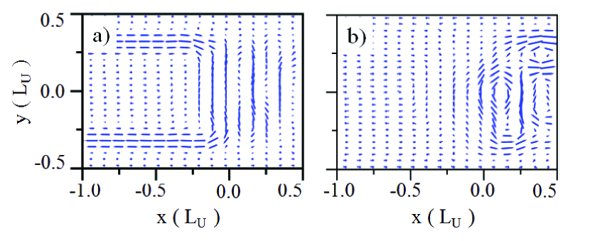
In Fig. 2a the superconductor is kept in a trivial phase with below a critical value, while in Fig. 2b it is in a topological phase because of the larger . While both figures are similar for weak magnetic fields, clear conductance oscillations arise for strong fields when the superconductor is in the trivial phase. These oscillations are of the same kind and share the same origin of those discussed in Ref. Takagaki (1998). In a semiclassical image the incident electrons are reflected as holes by the junction but the orbital effect bends their trajectories towards the junction again. This process is repeated along the transverse boundary creating a pattern that may enhance or suppress Andreev reflection against normal reflection. This effect can be seen as causing a complicated vortex structure in the junction (Fig. 3a). In the particular case of Fig. 2a the oscillations are seen only in the plateau of two active modes; however, higher chemical potentials allowing more active modes for strong magnetic fields would enable oscillations at different incident conditions.
On the other hand, when the superconductor is in the topological phase (Fig. 2b) the oscillations are fully suppressed in the two-mode plateau. This occurs because the vortex structure in the junction is dramatically modified with respect to the trivial case. In the topological phase a single dominant vortex is formed at the junction (Fig. 3b) irrespective of the strength of the magnetic field, eliminating this way any transverse structure that may enhance or suppress Andreev reflection. Note, too, that in the topological phase only one channel is open to Andreev reflection while the other one is reflected as normal electron-electron back scattering. The reason is that the topological number of the superconductor is only zero or one, larger values being forbidden in the D symmetry class of the Hamiltonian. As mentioned above, the complete suppression of magnetoconductance oscillations is only achieved in the two-mode plateau. Only one channel can be attached to the topological mode of the superconductor while the rest undergo Andreev or normal reflection by means of the usual physics of the trivial superconductor.
III.2 Chemical potential dependence
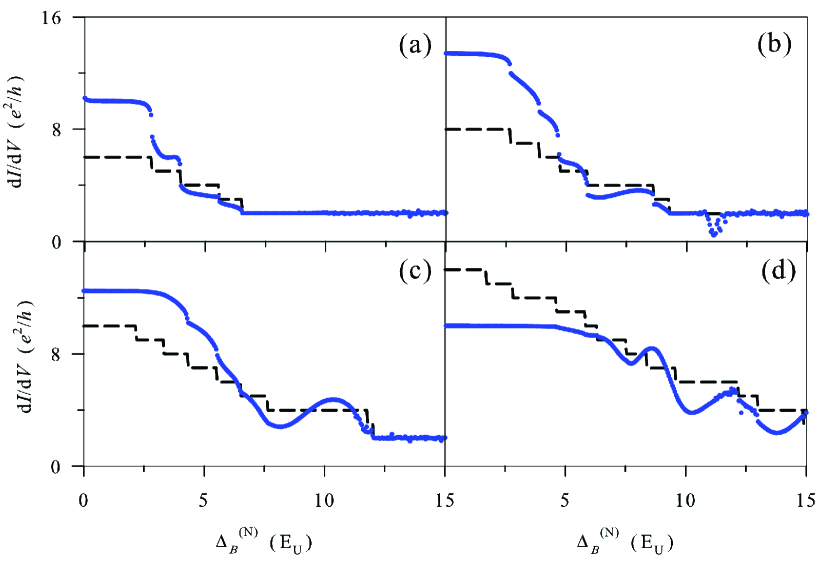
In Fig. 4 we show magnetoconductances of the NS junction when the chemical potentials of the normal and superconductor regions differ. The superconductor region is kept in the topological phase using the same parameters of Fig. 2b and the changes in chemical potential are only in the normal region. The main effect of increasing the N chemical potential is the displacement to higher magnetic fields of the plateau of two incident modes. Therefore the region of conductance oscillation suppression is consistently displaced to stronger magnetic fields too. Furthermore, for high enough N chemical potentials oscillations appear in regions where more than two incident modes are active. This is the usual physics of magnetoconductance oscillations with trivial superconductors and, as discussed above, the oscillation suppression affects only the channel that attaches to the topological mode of the superconductor.
IV Uniform magnetic fields
After having analyzed in the preceding section the topological suppression of oscillations with two independent tunable fields, we study now the more realistic case of the cleaved-edge nanowire in a uniform field (Fig. 1). Our model neglects the presence of localized states at the cleavage but it is enough to study the magnetoconductance oscillations. The modulus of the field may be above or below the critical value for the S lead. This critical value in presence of a 2D Rashba field was discussed in Ref. Osca and Serra (2015), generalizing previously known expressions Oreg et al. (2010); Lutchyn et al. (2010); San-Jose et al. (2014). It reads
| (11) |
where with are the 1D square well eigenenergies.
IV.1 Width dependence
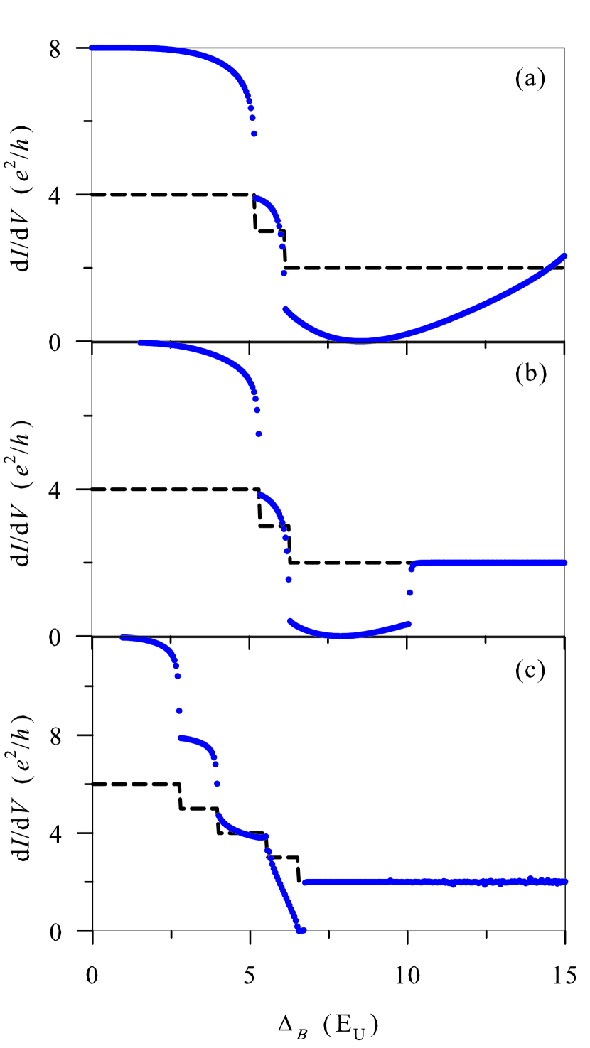
From Eq. (11) it is clear that we can adjust the critical field by changing the width of the nanowire. In this manner we can choose in which phase of the hybrid superconductor we find the plateau of two incident modes, where we expect to recover the behavior discussed in the preceding section. For instance, in Fig. 5a the nanowire is narrow enough to find the superconductor only in its trivial phase, while in Fig. 5c the nanowire is wide enough to find the plateau of two incident modes already in the topological region. We can also find an intermediate width in which oscillations are present at the beginning of the plateau and perfect suppression is seen in the rest of the plateau (Fig. 5b). Both regimes are separated in an abrupt way by the critical magnetic field. This is yet another proof of the topological suppression of magnetoconductance oscillations as it appears exactly at the expected critical value.
IV.2 Dependence on Rashba coupling
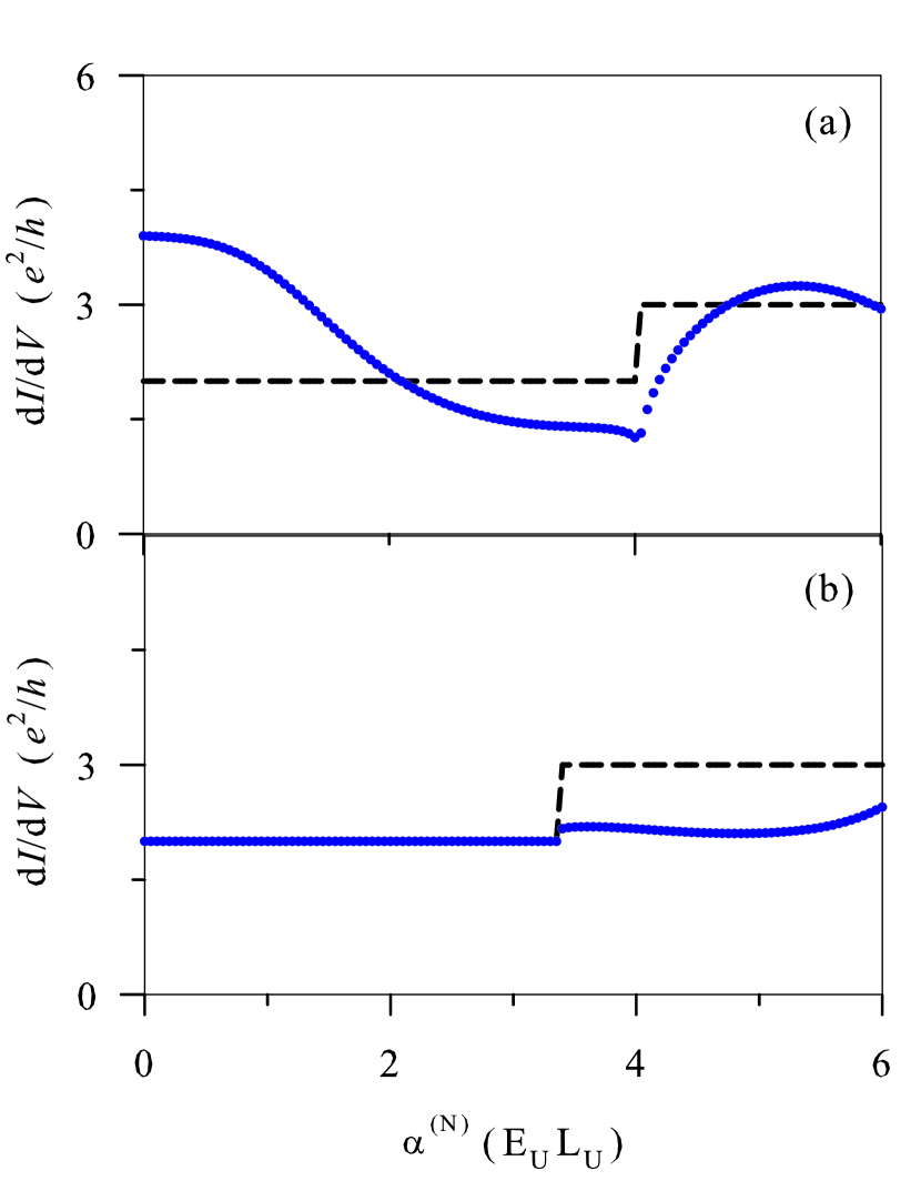
Another option to avoid using spatial variations of the magnetic field strength is tuning the intensity of the Rashba coupling. It is well known from spintronics that can be tuned using external electric gates Nitta et al. (1997). If the superconductor is in a trivial phase we observe variations in the conductance when changing the Rashba coupling in the normal side of the junction (Fig. 6a). On the contrary, if the superconductor is in the topological phase the conductance remains stuck at the quantized value provided that only two incident modes are active, as shown in Fig. 6b. We are assuming the existence of a gate that allow us to tune the Rashba coupling in the normal side of the junction independently of the superconductor side. With large enough ’s additional incident modes are active, thus generating the magnetoconductance variations observed at the right end of Fig. 6b.
Besides the two-mode restriction, it is important to also take into account that the value of the critical field, Eq. (11), changes with and the chemical potential in the superconductor side. In particular in Fig. 6 we have changed the overall chemical potential in the nanowire to control its phase while maintaining the homogeneous external magnetic field fixed.
V Robustness and generality
A relevant question is how robust is the suppression effect discussed in this work. Suppression of magnetoconductance oscillations occurs around zero energy, corresponding to vanishing potential bias on the NS junction. Moving away from zero energy (non zero bias) will eventually give rise to oscillations again. The suppression, however, is not a single-energy phenomenon fading away with infinitesimal energies but survives for energies within a finite range. The region around zero in which the suppression occurs gets wider with an increasing superconducting gap. On the other hand, it is known that trivial superconductors stop providing Andreev reflection for large gaps, and therefore any related magnetoconductance oscillations are also quenched for large gaps. Nevertheless, Andreev reflection with oscillation suppression is more robust and easier to find with large superconductor gaps in the topological phase of the superconductor.
We believe magnetoconductance suppression is a general property of any kind of topological superconductor. We have actually checked that with a p-wave superconductor in the topological phase Wimmer et al. (2010) the same kind of suppression of magnetoconductance variations is found. However, the main difference between p-wave and s-wave cases is that with p-wave superconductors it is no longer appropriate to think of topological oscillation suppression since oscillations are never present Yan and Wan (2014). This is because no Andreev reflection is found in the trivial phase of the p-wave. Andreev reflection is only found in the topological phase and therefore Takagaki-like oscillations are never found with p-wave superconductivity.

V.1 Lateral S phases
We next ask ourselves what happens to the magnetoconductance oscillations if the hybrid nanowire is laterally coupled to two different superconductors with different phases. One superconductor will be proximity coupled at one side of the wire while the other is in contact with the other side in the transverse direction. The middle region of the hybrid nanowire will remain normal. The resulting transverse structure is sketched in Fig. 7b. As shown in Fig. 7a, it is not needed that the superconductor pairing extends throughout the nanowire to obtain magnetoconductance oscillations, provided the superconductors are in the trivial phase. Furthermore, if the superconductors are in the topological phase we recover the same kind of oscillation suppression already seen for the full superconducting nanowire. Remarkably, in Fig. 7c we can see how a phase difference between both superconductors changes the shape of the conductance oscillations in the trivial phase, displacing the positions of maxima and minima. Despite these changes in the trivial phase, in panel 7d we can check again the robustness of the oscillation suppression, that is now resilient to superconductor phase changes in the two-mode plateau.
VI Conclusions
In this work we have shown how a superconductor in topological phase suppresses the magnetoconductance oscillations of NS junctions when the N wire sustains only two active modes. These oscillations are present under the same conditions but for the superconductor in the trivial phase. This result is due to the formation of a large vortex of probability current at the junction when the S wire enters the topological phase. We have analyzed the phenomenon from a theoretical point of view, assuming independently tunable fields on both junction sides, and we also studied more realistic scenarios of cleaved-edge wires in uniform fields. In the latter case it is possible to tune the suppression of the oscillations by changing the width of the nanowire.
We have proved the robustness of the oscillation suppression provided the superconductor topological phase is achieved. Similar oscillations can be found (or suppressed) tuning the Rashba coupling with an external electric field. With p-wave superconductors the same physics is found in the topological phase, although magnetoconductance oscillations are absent in the trivial phase and one can not properly speak of oscillation suppression. Finally, we have seen how the oscillations depend on the phase difference between two trivial superconductors proximity coupled with the nanowire in the transverse direction. In this case too, when the superconductors are in topological phase the suppression is robust and independent of their relative phase difference.
Acknowledgements.
This work was funded by MINECO-Spain (grant FIS2014-52564), CAIB-Spain (Conselleria d’Educació, Cultura i Universitats) and FEDER.References
- Ihn (2010) T. Ihn, Semiconductor nanostructures (Oxford, 2010).
- Beenakker (1992) C. W. J. Beenakker, Phys. Rev. B 46, 12841 (1992).
- Takagaki (1998) Y. Takagaki, Phys. Rev. B 57, 4009 (1998).
- Asano (2000) Y. Asano, Phys. Rev. B 61, 1732 (2000).
- Hoppe et al. (2000) H. Hoppe, U. Zülicke, and G. Schön, Phys. Rev. Lett. 84, 1804 (2000).
- Giazotto et al. (2005) F. Giazotto, M. Governale, U. Zülicke, and F. Beltram, Phys. Rev. B 72, 054518 (2005).
- Eroms et al. (2005) J. Eroms, D. Weiss, J. D. Boeck, G. Borghs, and U. Zülicke, Phys. Rev. Lett. 95, 107001 (2005).
- Chtchelkatchev and Burmistrov (2007) N. M. Chtchelkatchev and I. S. Burmistrov, Phys. Rev. B 75, 214510 (2007).
- Rakyta et al. (2007) P. Rakyta, A. Kormányos, Z. Kaufmann, and J. Cserti, Phys. Rev. B 76, 064516 (2007).
- Khaymovich et al. (2010) I. M. Khaymovich, N. M. Chtchelkatchev, I. A. Shereshevskii, and A. S. Mel’nikov, EPL (Europhysics Letters) 91, 17005 (2010).
- Carmier (2013) P. Carmier, Phys. Rev. B 88, 165415 (2013).
- Takagaki and Ploog (2000) Y. Takagaki and K. H. Ploog, Phys. Rev. B 62, 3766 (2000).
- Hsue et al. (2004) Y.-C. Hsue, T.-J. Yang, B.-Y. Gu, and J. Wang, Journal of the Physical Society of Japan 73, 1303 (2004), http://dx.doi.org/10.1143/JPSJ.73.1303 .
- Batov et al. (2007) I. E. Batov, T. Schäpers, N. M. Chtchelkatchev, H. Hardtdegen, and A. V. Ustinov, Phys. Rev. B 76, 115313 (2007).
- Sun (2008) G.-Y. Sun, J. Phys.: Condens. Matter 20, 325206 (2008).
- Fu and Kane (2008) L. Fu and C. L. Kane, Phys. Rev. Lett. 100, 096407 (2008).
- Oreg et al. (2010) Y. Oreg, G. Refael, and F. von Oppen, Phys. Rev. Lett. 105, 177002 (2010).
- Lutchyn et al. (2010) R. M. Lutchyn, J. D. Sau, and S. Das Sarma, Phys. Rev. Lett. 105, 077001 (2010).
- Alicea (2012) J. Alicea, Rep. Prog. Phys. 75, 076501 (2012).
- Leijnse and Flensberg (2012) M. Leijnse and K. Flensberg, Semicond. Sci. Technol. 27, 124003 (2012).
- Beenakker (2013) C. W. J. Beenakker, Annu. Rev. Condens. Matter Phys. 4, 113 (2013).
- Franz (2013) M. Franz, Nat Nano 8, 149 (2013).
- Stanescu and Tewari (2013) T. D. Stanescu and S. Tewari, Journal of Physics: Condensed Matter 25, 233201 (2013).
- Pfeiffer et al. (1990) L. Pfeiffer, K. W. West, H. L. Stormer, J. P. Eisenstein, K. W. Baldwin, D. Gershoni, and J. Spector, Applied Physics Letters 56, 1697 (1990), http://aip.scitation.org/doi/pdf/10.1063/1.103121 .
- Kjaergaard et al. (2012) M. Kjaergaard, K. Wölms, and K. Flensberg, Phys. Rev. B 85, 020503 (2012).
- Londergan et al. (1999) J. T. Londergan, J. P. Carini, and D. P. Murdock, Binding and scattering in two-dimensional systems: applications to quantum wires, waveguides and photonic crystals (Springer-Verlag, 1999).
- Osca and Serra (2015) J. Osca and L. Serra, Phys. Rev. B 91, 235417 (2015).
- Osca and Serra (2016) J. Osca and L. Serra, arXiv:1607.07635 (2016).
- Serra (2013) L. Serra, Phys. Rev. B 87, 075440 (2013).
- Blonder et al. (1982) G. E. Blonder, M. Tinkham, and T. M. Klapwijk, Phys. Rev. B 25, 4515 (1982).
- San-Jose et al. (2014) P. San-Jose, E. Prada, and R. Aguado, Phys. Rev. Lett. 112, 137001 (2014).
- Nitta et al. (1997) J. Nitta, T. Akazaki, H. Takayanagi, and T. Enoki, Phys. Rev. Lett. 78, 1335 (1997).
- Wimmer et al. (2010) M. Wimmer, A. R. Akhmerov, M. V. Medvedyeva, J. Tworzydło, and C. W. J. Beenakker, Phys. Rev. Lett. 105, 046803 (2010).
- Yan and Wan (2014) Z. Yan and S. Wan, New Journal of Physics 16, 093004 (2014).