Coupling quantum emitters in 2D materials with tapered fibers
Abstract
Realization of integrated photonic circuits on a single chip requires controlled manipulation and integration of solid-state quantum emitters with nanophotonic components. Previous works focused on emitters embedded in a three-dimensional crystals – such as nanodiamonds or quantum dots. In contrast, in this work we demonstrate coupling of a single emitter in a two-dimensional (2D) material, namely hexagonal boron nitride (hBN), with a tapered optical fiber and find a collection efficiency of the system is found to be 10 %. Furthermore, due to the single dipole character of the emitter, we were able to analyse the angular emission pattern of the coupled system via back focal plane imaging. The good coupling efficiency to the tapered fiber even allows excitation and detection in a fully fiber coupled way yielding a true integrated system. Our results provide evidence of the feasibility to efficiently integrate quantum emitters in 2D materials with photonic structures.
keywords:
2D materials, hexagonal boron nitride, single photon emitters, tapered fiber, nanofiberKyoto University] Department of Electronic Science and Engineering, Kyoto University, 615-8510 Kyoto, Japan Kyoto University] Department of Electronic Science and Engineering, Kyoto University, 615-8510 Kyoto, Japan UTS] School of Mathematical and Physical Sciences, University of Technology Sydney, Ultimo, New South Wales 2007, Australia UTS] School of Mathematical and Physical Sciences, University of Technology Sydney, Ultimo, New South Wales 2007, Australia Kyoto University] Department of Electronic Science and Engineering, Kyoto University, 615-8510 Kyoto, Japan
![[Uncaptioned image]](/html/1701.02696/assets/toc.png)
Atomically thin two-dimensional (2D) materials are garnering major attention in a variety of emerging applications in nanophotonics and optoelectronics 1, 2 spanning low threshold lasing 3, sub-diffraction imaging 4, 5, valleytronics 6, 7, and efficient light emitting diodes 8, 9. In particular, hexagonal boron nitride (hBN) has recently emerged as a promising layered material that hosts optically stable single photon emitters that operate at room temperature 10, 11, 12, 13. These defects have a narrow emission linewidth from the ultraviolet to the near infrared spectral range, are bright, and can be excited by two-photon excitation 14. These properties make them promising candidates for applications in (bio)-sensing 15, nanophotonics 16, and quantum information science 17.
However, in order to employ these emitters in applications, e.g., as single photon sources, it is necessary to efficiently extract the emitted photons 18. While usage of solid immersion lenses 19 and dielectric antennas 20 has been demonstrated, these approaches do not offer a path to scalability and suffer from complicated output modes. A promising direction to overcome this problem is using near-field coupling to tapered optical fibers 21, 22, 23, where the photons get directly emitted into a guided mode inside the fiber. In these geometries, coupling efficiencies of over 20 % can be reached and even higher efficiencies are possible by combining the tapered fibers with optical cavities, such as nanofiber Bragg cavities (NFBCs) 24, 25, 26.
In this letter, we demonstrate unprecedented results of coupling quantum emitters embedded in layered hBN to a tapered optical fiber. We show efficient collection of light emitted by a single photon emitter into the optical fiber and prove that the quantum nature of light is maintained throughout when the light is guided through the fiber. We further analyze the collection efficiency in detail by taking into account the non-isotropic emission of a dipole emitter.
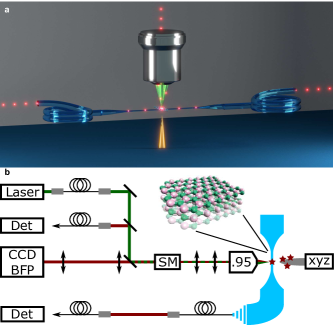
A sketch of the setup is shown in Figure 1 (see Methods for detailed description). The setup consists of a home-built beam-scanning confocal microscope equipped with a spectrometer and avalanche photodiodes for photon correlation measurements. The emitters in hBN (see Methods) are excited using pulsed or continuous wave lasers at a wavelength of . A tapered optical fiber with a radius of is positioned in front of the objective lens with a numerical aperture (NA) of 0.95. One end of the fiber is spliced to a longer fiber from which the light is coupled out in order to perform filtering before it is sent to the detectors.
To transfer the hBN flakes that host the quantum emitters onto the tapered fiber a sharp tungsten tip driven by a piezo positioner is used 27. The hBN flakes are lifted off the silicon substrate with the tip. Subsequently, the flakes are then placed onto the fiber by approaching the tungsten tip to the tapered region of the fiber. After successful transfer of an hBN flake, room-temperature optical measurements were carried out.
We first compare the emission properties of the hBN sources into free space using the high NA objective lens with the collection through the fiber. Figure 2(a) and (b) show the room-temperature spectra of the light collected through the objective lens and through the fiber, respectively. In both spectra, two peaks are visible (at and ), most likely corresponding to two individual single emitters. In the following, the emitter at will be investigated in detail. Unless otherwise stated, a bandpass filter between and is used. The full width at half maximum (FWHM) of the peak is approximately . Notably, in both cases, namely through the fiber and via the high NA objective, the spectra are very similar, and the sharp lines of the emitter is clearly visible. The minor differences can be explained by different coupling efficiencies to the fiber and the objective lens and by fluorescence coming from pump light entering the silica fiber.
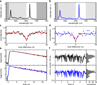
To prove that the emitter is indeed a single photon source, the second order autocorrelation function, , is recorded. Figure 2(c) and (d) show these antibunching measurements of the light collected through the objective lens and through the fiber’s end, respectively. The measurements were carried out using the bandpass filter in order to only collect light from the sharp line at . Both curves show a pronounced dip at zero time delay (t=0), confirming the single photon nature of the light. This clearly proves that the coupling of a defect in a two-dimensional material to the fiber and extraction of its photons is successful.
In Figure 2(e) lifetime measurements for the free space collection and collection via the fiber are shown. The lifetimes through the objective and the fiber are and , respectively. As expected, these lifetimes are nearly identical, as it is the same emitter. The small differences can again be explained by different contributions of background light. To avoid most of these contributions, the fit was carried out to the data starting from after the excitation laser pulse.
Finally, we analyze the temporal stability of this emitter by recording the intensity count rate as a function of time. The corresponding measurements are shown in Figure 2(f). As expected, the emission is modulated in a very similar manner when collected via both outputs, namely air objective (upper part) and fiber (lower part). The observed sharp steps in both cases are an indication that this modulation is not caused by the fiber vibrating and drifting through the laser focus, where the modulation would be expected to be continuous. This indicates a blinking behavior of the emitter, that was also be found for some emitters on the substrate.
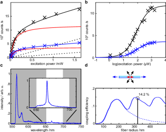
To show the high coupling efficiency of the quantum emitter to the fiber, saturation measurements were carried out (see Figure 3(a-c)). The saturation curves follow the Equation 28:
| (1) |
with the pump laser intensity , the emission rate at saturation , the saturation intensity , and an additional linear background with coefficient . From fits to the data saturated emission rates of and were found for collection through the objective lens and one end of the fiber, respectively. For the fit to the confocal data, due to the higher noise, the saturation intensity was fixed to , which is the value extracted from the fit to the data through the fiber, that exhibits lower noise levels.
Since the measurements for the count rate at the tapered fiber were only carried out on one end, in order to exclude reflections in the open end of the fiber, the reflectivity of the whole fiber (including the reflection from the facet) was measured. A value below for the reflectivity below 0.1 was found indicating that this is not the case and the measured count rate stems indeed from the photons emitted in one end.
Figure 3(c) shows the emission spectrum, excited with a laser beam that is propagating through the fiber. In this configuration, the propagating laser beam can excite background fluorescence inside the fiber. Nevertheless, due to a high coupling efficiency for excitation and emitted photons, and the use of a pure silica core tapered fiber, the defect’s emission can be detected as a bright line at . Excitation and detection through the fiber will enable the system to serve as an integrated single photon source in quantum networks.
Figure 3d shows the results of numerical simulations of the coupling efficiency for a dipole oriented longitudinal along the fiber yielding an efficiency of 14.2 % for the fiber diameter used in the experiment.
To get more insight into the coupling of hBN defect to the nanofiber, we performed measurements of the polarisation dependence of excitation and emission. The corresponding measurements are shown in Figure 4(a-c). In Figure 4(a,b), the polarisation of the excitation laser is rotated and the emission collected through the objective and through the fiber, respectively. The observed pattern suggests that the transition dipole excited by the laser lies in parallel with the nanofiber. Figure 4(c) shows the polarisation of the photons collected through the objective when the pump laser is coupled into the fiber (i.e. exciting the defect through the fiber). Here, the polarisation has a reduced visibility, which could be an indication that the line at is excited indirectly 12.
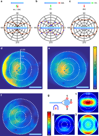
By coupling single photon emitters to photonic structures, such as the nanofiber used here, not only new decay channels are provided, but also the overall emission pattern is altered. This can be investigated by imaging the back focal plane (BFP) of the microscope objective. In the BFP, the angle of the emission to the optical axis is directly visible. Figure 4(d-f) shows BFP images of the nanofiber coupled with he hBN flake in three different configurations. First, in Figure 4(d), in order to check the general scattering properties, broadband light from a halogen lamp is coupled into the fiber and the scattered light observed. Light leaking from the fiber is visible under high angles at the left side of the image. In addition, scattering from the particle hosting the hBN flake can be seen in the middle. Second, in Figure 4(e), the BFP image is shown when exciting through the fiber. Due to contributions of other sources of light at other wavelengths a near isotropic emission is found. Finally, to only investigate the light from the single defect at wavelength, in Figure 4(f) the fluorescence when using the bandpass is shown. Two lobes are visible, separated by a minimum along the fiber axis. This situation can be compared to the numerical calculation shown in Figure 4(g) (see Methods).
In these calculations, the back focal plane intensity pattern is investigated for a dipole in parallel orientation at positions on top of the fiber, at the middle position, and at the bottom position (labeled 1-3 respectively). The data shown is is normalized to each panel’s maximum and the fraction of the total emitted power falling in the numerical aperture of 0.95 used in the experiment is 0.22, 0.22, and 0.51, respectively. This shows that the position of the dipole has a dramatic effect on the number of photons that can be collected with an objective lens in free space that has to be taken into account when calculation the coupling efficiency to the nanofiber. The assumption of isotropic emission of the emitter, while often made, is a relatively coarse approximation, as we will investigate later in this paper. In our case, the pattern when the dipole sits at the middle of the fiber is closest to the measured result in Figure 4(f). Hence, the calculated free space collection efficiency is .
The values found for the collection efficiency differ by more than a factor of two for different dipole positions. It is therefore illustrative to compare them with the result when assuming isotropic emission of the dipole. In this case, the 0.95 NA collection lens collects of the full solid angle. This would – using the value of for the coupling efficiency to the fiber from the calculations shown in Figure 3(d) – yield a value for the microscope collection efficiency of .
In order to get an experimental value for the coupling efficiency in the fiber, the transmission of the optics has to be known (see Methods). Experimentally, we found a relative transmission for the two different paths of . The coupling efficiency to the fiber is then given by:
| (2) |
where the factor of 2 accounts for the fact that light is emitted to both ends of the fiber.
This shows, that the fiber coupled system is able to achieve a similar collection efficiency as a high NA objective lens, while having the advantage of being directly fiber coupled and offers alignment free collection. With the use of nanofiber Bragg cavities, this value can even surpass high NA objective lenses and efficiencies over 80 % are expected 26.
The value of the coupling efficiency of 10 % found here is consistent with the findings of other results using other emitters such as quantum dots 22, 21 or defect centers 29, 23. While those measurements were performed using a single mode nanofiber, here a fibre in the multimode regime was used. In this regime the total coupling efficiency can be even higher than in the single mode regime 30, 31, what can be seen in Figure 3(d). For the peak for small fiber diameters (single mode regime) is smaller than the other two peaks for a larger radius.
In conclusion, we realized an integrated photonic system where a quantum emitter in a 2D material, layered hBN is coupled to a tapered optical fiber. We achieved highly efficient coupling to the fiber with an efficiency of 10 % and were able to prove the quantum nature of the light emitted. BFP imaging of the emission dipole as well as polarization measurements confirm the efficient coupling of the quantum emitter to the tapered fiber and show that the dipolar emission pattern of the emitter has to be taken into account when measuring the coupling efficiency. The highly efficient coupling observed even allows for excitation of the emitter and collection through the same fiber, establishing a fully fiber integrated system. Our results pave the way for promising applications in integrated quantum photonics using single emitters in hBN.
Acknowledgment
We thank Kali Nayak for help with the low fluorescent nanofibers, Syun Suezawa for help with Figure 1 and Hironaga Maruya and Atsushi Fukuda for support. The work was further supported by MEXT/JSPS KAKENHI Grant Number 26220712, 21102007, JST CREST project, and Special Coordination Funds for Promoting Science and Technology AWS thanks funding by the Japanese Society for the Promotion of Science through a fellowship for overseas researchers. Financial support from the Australian Research Council (IH150100028, DE130100592) and the Asian Office of Aerospace Research and Development grant FA2386-15-1-4044 are gratefully acknowledged.
Methods
hBN samples
A native oxide Si (100) substrate was cleaned thoroughly with acetone, isopropanol, and ethanol before
drop-casting of ethanol solution containing pristine hBN flakes (Graphene Supermarket) of
approximately in diameter and
of height onto silicon substrates. The completely dried
sample was then loaded into a fused-quartz tube in a tube furnace (Lindberg Blue). The tube was
evacuated to low vacuum ( ) by using a rough pump then purged for
under of Ar
with pressure regulated at . The substrate was then annealed at
for under of
argon. This thermal treatment step is employed to increase the optically active defect density 32.
Tapered fibers
The tapered fiber is fabricated by heating an optical fiber (0.25Z-U, Sumitomo Electric) with a ceramic heater
to a temperature of about .
The fiber was stretched for with speeds from
resulting in an overall distance of .
With this, a waist diameter of about was achieved.
The transmission of the fiber stayed (apart from mode beating expected in multimode fibers)
close to unity during this process.
Setup
The experimental setup used (shown in Figure 1) consists of a home build confocal microscope and a
manipulator. The manipulator consists of a sharp tungsten tip (TP-0002, Micro Support) and a three axis piezo stage (TRITOR 100, Piezosystem Jena).
The microscope objective used (MPlanApo N 100x/0.95, Olympus) has a numerical aperture of 0.95 and is mounted on a one axis piezo stage
(TRITOR 100 SG, Piezosystem Jena) to adjust the focus. Scanning is achieved by a scanning mirror unit (GVS002, Thorlabs) and the
excitation lasers used are a wavelength continuous wave laser (LBX-532, Oxxius) and a picosecond
laser at the same wavelength (Katana, Onefive) for pulsed measurements. Detection is
done via two avalanche photodiodes (SPCMM-AQRH-14-FC, Perkin Elmer) behind a fiber beam splitter connected to a counting module
(Time Harp 200, Picoquant) or by a Peltier cooled camera (DU420-OE, Andor) behind a monochromator (Oriel MS257). For
back focal plane imaging, the back focal plane is imaged on a Peltier cooled camera (PIXIS 1024, Princeton Instruments).
Transmissions of the microscope and fiber setup was measured to be 0.56 (without bandpass filter,
fiber in-coupling, and microscope objective) and 0.7 for the setup used for filtering the light from the fiber
(not including fiber in- and out-coupling).
The transmission of the bandpass filter cancels out as it
is used in both setups and the difference in fiber coupling is estimated to be 90 %. From the
manufacturer, the transmission of the transmission of the microscope objective is given as 90 %
by the manufacturer. The relative transmission is hence .
FDTD simulations
In order to analyze the far-field pattern and the corresponding collection efficiency,
three dimensional finite-difference time-domain (FDTD) simulations were performed on a commercial package
(FDTD Solutions, Lumerical). The calculation region (length width height) were set to
. An automatic nonuniform mesh and the material properties of
SiO2 provided by the software were used in the calculation. A single dipole source was slightly outside
() the surface of the fiber. Perfectly matched layers (PML) were employed as absorbing boundary
conditions. The far-field pattern was calculated from the top side of the calculation region.
The coupling efficiency to the nanofiber is calculated by comparing the total emission a dipole with the power coupled into the fiber measured with a sized monitor at the end of the nanofiber.
References
- Mak and Shan 2016 Mak, K. F.; Shan, J. Photonics and optoelectronics of 2D semiconductor transition metal dichalcogenides. Nature Photonics 2016, 10, 216–226
- Novoselov et al. 2016 Novoselov, K.; Mishchenko, A.; Carvalho, A.; Neto, A. C. 2D materials and van der Waals heterostructures. Science 2016, 353, aac9439
- Wu et al. 2015 Wu, S.; Buckley, S.; Schaibley, J. R.; Feng, L.; Yan, J.; Mandrus, D. G.; Hatami, F.; Yao, W.; Vuckovic, J.; Majumdar, A.; et al., Monolayer semiconductor nanocavity lasers with ultralow thresholds. Nature 2015, 520, 69–72
- Caldwell et al. 2014 Caldwell, J. D.; Kretinin, A. V.; Chen, Y.; Giannini, V.; Fogler, M. M.; Francescato, Y.; Ellis, C. T.; Tischler, J. G.; Woods, C. R.; Giles, A. J.; et al., Sub-diffractional volume-confined polaritons in the natural hyperbolic material hexagonal boron nitride. Nature communications 2014, 5, 5221–5221
- Dai et al. 2014 Dai, S.; Fei, Z.; Ma, Q.; Rodin, A.; Wagner, M.; McLeod, A.; Liu, M.; Gannett, W.; Regan, W.; Watanabe, K.; et al., Tunable phonon polaritons in atomically thin van der Waals crystals of boron nitride. Science 2014, 343, 1125–1129
- Yang et al. 2016 Yang, W.; Shang, J.; Wang, J.; Shen, X.; Cao, B.; Peimyoo, N.; Zou, C.; Chen, Y.; Wang, Y.; Cong, C.; et al., Electrically tunable valley-light emitting diode (vLED) based on CVD-grown monolayer WS2. Nano letters 2016, 16, 1560–1567
- Sie et al. 2015 Sie, E. J.; McIver, J. W.; Lee, Y.-H.; Fu, L.; Kong, J.; Gedik, N. Valley-selective optical Stark effect in monolayer WS2. Nature materials 2015, 14, 290–294
- Clark et al. 2016 Clark, G.; Schaibley, J. R.; Ross, J. S.; Taniguchi, T.; Watanabe, K.; Hendrickson, J. R.; Mou, S.; Yao, W.; Xu, X. Single Defect Light Emitting Diode in a van der Waals Heterostructure. Nano letters 2016, 16, 3944–3948
- Withers et al. 2015 Withers, F.; Del Pozo-Zamudio, O.; Mishchenko, A.; Rooney, A.; Gholinia, A.; Watanabe, K.; Taniguchi, T.; Haigh, S.; Geim, A.; Tartakovskii, A.; et al., Light-emitting diodes by band-structure engineering in van der Waals heterostructures. Nature materials 2015, 14, 301–306
- Tran et al. 2016 Tran, T. T.; ElBadawi, C.; Totonjian, D.; Lobo, C. J.; Grosso, G.; Moon, H.; Englund, D. R.; Ford, M. J.; Aharonovich, I.; Toth, M. Robust multicolor single photon emission from point defects in hexagonal boron nitride. ACS Nano 2016, 10, 7331–7338
- Bourrellier et al. 2016 Bourrellier, R.; Meuret, S.; Tararan, A.; Stephan, O.; Kociak, M.; G. Tizei, L. H.; Zobelli, A. Bright UV single photon emission at point defects in h-BN. Nano letters 2016, 16, 1317–4321
- Jungwirth et al. 2016 Jungwirth, N. R.; Calderon, B.; Ji, Y.; Spencer, M. G.; Flatt, M. E.; Fuchs, G. D. Temperature Dependence of Wavelength Selectable Zero-Phonon Emission from Single Defects in Hexagonal Boron Nitride. Nano Lett. 2016, 16, 6052–6057
- Chejanovsky et al. 2016 Chejanovsky, N.; Rezai, M.; Paolucci, F.; Kim, Y.; Rendler, T.; Rouabeh, W.; Fa?varo de Oliveira, F.; Herlinger, P.; Denisenko, A.; Yang, S.; et al., Structural Attributes and Photodynamics of Visible Spectrum Quantum Emitters in Hexagonal Boron Nitride. Nano Letters 2016, 16, 7037–7045
- Schell et al. 2016 Schell, A. W.; Tran, T. T.; Takashima, H.; Takeuchi, S.; Aharonovich, I. Non-linear excitation of quantum emitters in hexagonal boron nitride multiplayers. APL Photonics 2016, 1, 091302–091302
- Helmchen and Denk 2005 Helmchen, F.; Denk, W. Deep tissue two-photon microscopy. Nature methods 2005, 2, 932–940
- Gaponenko 2010 Gaponenko, S. V. Introduction to nanophotonics; Cambridge University Press, 2010; pp –
- Weber et al. 2010 Weber, J.; Koehl, W.; Varley, J.; Janotti, A.; Buckley, B.; Van de Walle, C.; Awschalom, D. D. Quantum computing with defects. Proceedings of the National Academy of Sciences 2010, 107, 8513–8518
- Aharonovich et al. 2016 Aharonovich, I.; Englund, D.; Toth, M. Solid-state single-photon emitters. Nature Photonics 2016, 10, 631–641
- Mansfield and Kino 1990 Mansfield, S. M.; Kino, G. S. Solid immersion microscope. Applied Physics Letters 1990, 57, 2615–2616
- Lee et al. 2011 Lee, K. G.; Chen, X. W.; Eghlidi, H.; Kukura, P.; Lettow, R.; Renn, A.; Sandoghdar, V.; Götzinger, S. A planar dielectric antenna for directional single-photon emission and near-unity collection efficiency. Nature Photonics 2011, 5, 166–169
- Yalla et al. 2012 Yalla, R.; Le Kien, F.; Morinaga, M.; Hakuta, K. Efficient channeling of fluorescence photons from single quantum dots into guided modes of optical nanofiber. Physical review letters 2012, 109, 063602–063602
- Fujiwara et al. 2011 Fujiwara, M.; Toubaru, K.; Noda, T.; Zhao, H.-Q.; Takeuchi, S. Highly Efficient Coupling of Photons from Nanoemitters into Single-Mode Optical Fibers. Nano Letters 2011, 11, 4362–4365
- Liebermeister et al. 2014 Liebermeister, L.; Petersen, F.; Munchow, A. v.; Burchardt, D.; Hermelbracht, J.; Tashima, T.; Schell, A. W.; Benson, O.; Meinhardt, T.; Krueger, A.; Stiebeiner, A.; Rauschenbeutel, A.; Weinfurter, H.; Weber, M. Tapered fiber coupling of single photons emitted by a deterministically positioned single nitrogen vacancy center. Applied Physics Letters 2014, 104, 031101–031101
- Yalla et al. 2014 Yalla, R.; Sadgrove, M.; Nayak, K. P.; Hakuta, K. Cavity quantum electrodynamics on a nanofiber using a composite photonic crystal cavity. Physical review letters 2014, 113, 143601–143601
- Schell et al. 2015 Schell, A. W.; Takashima, H.; Kamioka, S.; Oe, Y.; Fujiwara, M.; Benson, O.; Takeuchi, S. Highly efficient coupling of nanolight emitters to a ultra-wide tunable nanofibre cavity. Scientific reports 2015, 5, 9619–9619
- Takashima et al. 2016 Takashima, H.; Fujiwara, M.; Schell, A. W.; Takeuchi, S. Detailed numerical analysis of photon emission from a single light emitter coupled with a nanofiber Bragg cavity. Optics Express 2016, 24, 15050–15058
- Fujiwara et al. 2016 Fujiwara, M.; Yoshida, K.; Noda, T.; Takashima, H.; Schell, A. W.; Mizuochi, N.; Takeuchi, S. Manipulation of single nanodiamonds to ultrathin fiber-taper nanofibers and control of NV-spin states toward fiber-integrated lambda-systems. Nanotechnology 2016, 27, 455202–455202
- Novotny and Hecht 2012 Novotny, L.; Hecht, B. Principles of nano-optics; Cambridge university press, 2012
- Schroeder et al. 2012 Schroeder, T.; Fujiwara, M.; Noda, T.; Zhao, H.-Q.; Benson, O.; Takeuchi, S. A nanodiamond-tapered fiber system with high single-mode coupling efficiency. Optics express 2012, 20, 10490–10497
- Kumar et al. 2015 Kumar, R.; Gokhroo, V.; Deasy, K.; Maimaiti, A.; Frawley, M. C.; Phelan, C.; Chormaic, S. N. Interaction of laser-cooled 87Rb atoms with higher order modes of an optical nanofibre. New Journal of Physics 2015, 17, 013026
- Shi et al. 2016 Shi, Q.; Sontheimer, B.; Nikolay, N.; Schell, A.; Fischer, J.; Naber, A.; Benson, O.; Wegener, M. Wiring up pre-characterized single-photon emitters by laser lithography. Scientific Reports 2016, 6, 31135–31135
- Tran et al. 2016 Tran, T. T.; Bray, K.; Ford, M. J.; Toth, M.; Aharonovich, I. Quantum emission from hexagonal boron nitride monolayers. Nature nanotechnology 2016, 11, 37–41