Photostrictive two-dimensional materials in the monochalcogenide family
Abstract
Photostriction is predicted for SnS and SnSe monolayers, two-dimensional ferroelectrics with rectangular unit cells (the lattice vector is larger than ) and an intrinsic dipole moment parallel to . Photostriction in these two-dimensional materials is found to be related to the structural change induced by a screened electric polarization in the photoexcited electronic state (i.e., a converse piezoelectric effect) that leads to a compression of and a comparatively smaller increase of for a reduced unit cell area. The structural change documented here is ten times larger than that observed in BiFeO3, making monochalcogenide monolayers an ultimate platform for this effect. This structural modification should be observable under experimentally feasible densities of photexcited carriers on samples that have been grown already, having a potential usefulness for light-induced, remote mechano-opto-electronic applications.
A truly novel opto-mechanical coupling in two-dimensional (2D) ferroelectric materials awaits to be discovered. Photostriction –the creation of non-thermal strain upon illumination Tatsuzaki et al. (1966); V. M. Fridkin et al. (1967); Kundys (2015); Paillard et al. (2016a)– has been well-documented in three-dimensional ferroelectrics such as SbSI Dogan et al. (2001) and BiFeO3 Kundys et al. (2010a, 2012). It has been suggested to be driven by the large voltage build-up caused by a photovoltaic effect and the resulting converse piezoelectricity Fridkin (1979), and it may be useful for applications such as remotely-switchable memory devices V. Iurchuk et al. (2016) and light-induced actuators Paillard et al. (2016b). The earliest studied photostrictive material, SbSI, transitions from a ferroelectric onto a paraelectric at a critical temperature K. As photostrictive effects are larger in the ferroelectric phase, can be increased above 300 K on SbSI ceramics which have smaller domain sizes and display a non-uniform stoichiometry nevertheless. The photostriction response time increases with sample thickness due to a reduced penetration depth, being a few seconds on bulk samples Dogan et al. (2001). On the other hand, ferroelectric films show photostriction within a few picoseconds Jin et al. (2012); D. Daranciang et al. (2012); H. Wen et al. (2013); Ruello et al. (2012); Lejman et al. (2014), and even when the photoexcited electron-hole pair is localized D. Schick et al. (2014); Wen et al. (2015).
The growing interest on the interactions of light with 2D materials Castellanos-Gomez (2016); W. Xiaomu et al. (2015); Basov et al. (2016); Basov and Fogler (2016) makes a study of illumination leading to non-trivial structural deformations an interesting and timely endeavor. As long as a photoexcited state induces some amount of charge redistribution –which is a quite reasonable physical assumption– any material is expected to change shape as the structure is let to relieve the stress induced by the photoexcited carriers. Here, the surprising result is the rather large magnitude of such structural change for 2D ferroelectrics, that originates from an inverse piezoelectric effect upon illumination.
Two-dimensional ferroelectrics in the group IV monochalcogenide family (GeS, GeSe, SnS, SnSe, among others) Tritsaris et al. (2013); Singh and Hennig (2014); Zhu et al. (2015); M. Mehboudi et al. (2016); K. Chang et al. (2016); Wu and Zeng (2016); Mehboudi et al. (2016); Hanakata et al. (2016); Fei et al. (2016); Wang and Qian (2016) undergo a ferroelectric-to-paraelectric transition with a transition temperature that is tunable by atomic number M. Mehboudi et al. (2016). Following the numerical approach proven to capture photostriction of BiFeO3 Paillard et al. (2016b), the photostriction of SnS and SnSe is successfully predicted hereby. This effect could be readily observed in recent experimental setups as the one in Ref. K. Chang et al. (2016).
The challenge at hand and the computational approach are described first. Then, the two direct optical transitions to be employed to demonstrate the effect are motivated, and the anisotropic change of lattice parameters (photostriction) upon photoexcitation is documented. The decrease of the dipole moment and unit cell area seen in our numerical results are explained in terms of a photoinduced inverse piezoelectric effect and electronic pressure afterwards.
The concept is straightforward: one creates the effect of a direct optical transition at the valence and conduction band edges, allowing the structure to relax the forces created in the photoexcited state. In practice, capturing the effect requires approximations: specifically, the accuracy in forces needed to observe photostriction makes the Bethe-Salpeter approach Hedin (1965); Hybertsen and Louie (1986) –the technique of choice for optical excitations in materials of reduced dimensionality– prohibitively expensive, and the same could be said of a time-dependent approach to the problem Ullrich (2012). Indeed, photostriction under a density of photoexcited carriers changes lattice parameters () to within in bulk samples Kundys (2015), making for a prohibitively expensive optimization of the electron-hole-pair hosting structure ( here).
However, the recent discovery of ferroelectricity in monochalcogenide monolayers M. Mehboudi et al. (2016); K. Chang et al. (2016) gives an opportunity to extend this well-known effect into 2D materials, and the structural deformation in photoexcited SnS and SnSe monolayers will be demonstrated using the same numerical technique Paillard et al. (2016b) that successfully reproduces the experimentally observed photostriction of BiFeO3 Kundys et al. (2010b).
Görling formulated the interacting, photoexcited Hamiltonian as a model non-interacting DFT Hamiltonian Görling (1999), and the -self-consistent-field (SCF) method is a realization of Görling’s approach that assumes a one-to-one correspondence between the excited states of a Kohn-Sham Hamiltonian and the real system Martin (2004). It creates a population imbalance akin to that produced from illumination, by depleting a finite number of electrons in the valence band and promoting them onto higher energy bands. SCF calculations of excited states for systems with reduced dimensions abound (e.g., Refs. Gavnholt et al. (2008); Kitaoka et al. (2013); Nawa et al. (2016)), and the SCF method as implemented in the ABINIT code X. Gonze et al. (2009) is employed to predict structural effects of direct optical transitions at the valley edges of ferroelectric SnS and SnSe monolayers here. Calculations were performed with GBRV projected-augmented-wave Blöchl (1994) pseudopotentials Garrity et al. (2014) of the PBE type Perdew et al. (1996), which are known to underestimate the electronic band gap. Nevertheless, additional corrections make it prohibitive to demonstrate the effect within computational constraints.
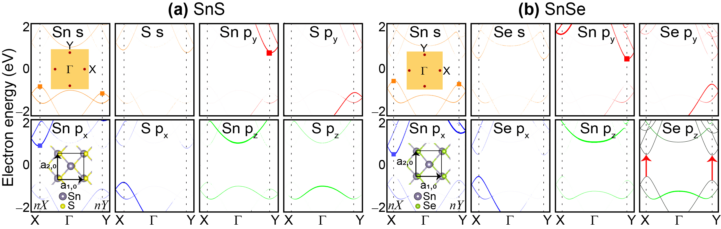
Figure 1 shows the electronic structure decomposed in states with , , or orbital symmetry and belonging to a specific atomic species (Sn or S in Fig. 1(a), and Sn or Se in Fig. 1(b)). Line thicknesses reflect the relative probability of finding a given orbital symmetry for a given band and chemical element. The lattice parameters for the ground-state structure shown as an inset in Fig. 1(a) (prior to photoexcitation; i.e., ) are Å and Å for the SnS monolayer. For the SnSe monolayer (inset in Fig. 1(b)) Å and Å. The unit cell area is .
Optical transitions require non-zero matrix elements for wavefunctions with symmetry in the conduction band and symmetry in the valence band (, , ). In SnS, there are two main valleys near the corners of the first Brillouin zone that are located at 0.390 and 0.415 (vertical dotted lines in Fig. 1(a)) and labeled and as shorthand for points located “near the high-symmetry point” and “near the high-symmetry point,” respectively ( and are reciprocal lattice vectors). These valleys are located at 0.415 and 0.415 for SnSe (Fig. 1(b)).
According to Fig. 1, the group-IV element (Sn) has a larger probability to have an orbital symmetry at the and valence band edges for both SnS and SnSe monolayers (as emphasized by orange rectangles at such band edges). Similarly, a large probability is carried by Sn orbitals with () symmetry at the () conduction valley edge (red rectangles). This way, the non-zero matrix element originates from a Sn intra-atomic direct optical transition with linearly-polarized absorption band edges Mehboudi et al. (2016); Gomes et al. (2016).
Illumination by pulsed laser sources can generate photoexcited carrier density fluences as high as /cm2 on MoS2 samples Lui et al. (2014). It will be shown that a much smaller density is needed for the effect being presently described to be experimentally achievable, after discussing the point mesh employed in calculations.
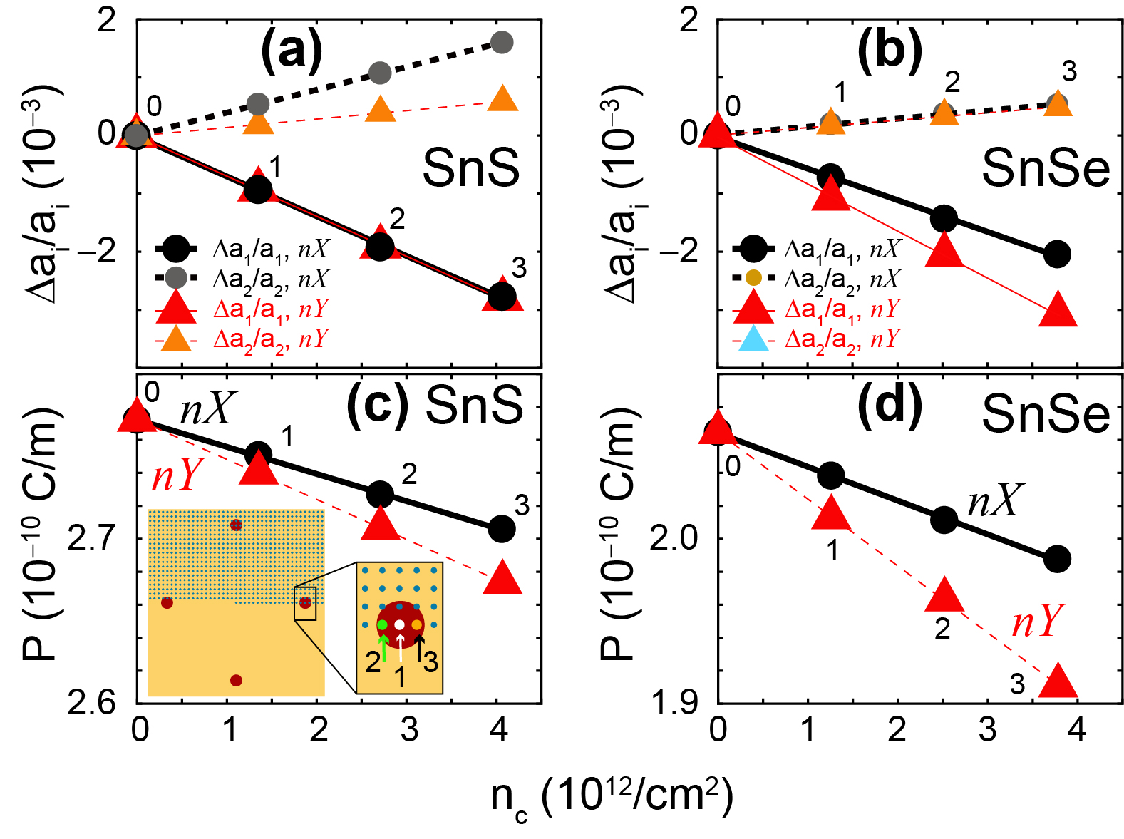
Considering spin-orbit coupling (SOC), a regular 2D mesh containing equally-weighted points yields a density of charge carriers per band per point per unit cell. The point mesh with –shown as an inset in Fig. 2(c)– permits creating /cm2 excited charge carriers per band per unit cell. Here, the factor of four is due to the symmetry of the point mesh shown at the inset, and because carriers from two bands immediately below the bandgap are excited into two bands right above the bandgap that are slightly split due to SOC; the dependence of on or allows for a gradual increment of photoexcited carriers. Recalling that photostrition of bulk samples results on Kundys (2015); Kundys et al. (2010b); Paillard et al. (2016b), a demanding relaxation limit for structural forces of Ha/Bohr and an energy cutoff of 40 Ha were employed in our calculations.
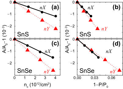
Figures 2(a) and 2(b) display a decrease of () and an increase of () for both SnS and SnSe monolayers. More specifically, the ratio is equal to for the transition and at the transition for SnS. In SnSe, () and (). (For reference, Poisson ratios are 0.36 and 0.42 for SnS and SnSe, respectively Fei et al. (2015).) In addition, a compression of the unit cell area versus () is illustrated in Figs. 3(a,c). Figs. 2(a-b) contain the first prediction of photostrictive effects in 2D materials; they open a completely unexplored door for studies of coupled mechano-opto-electronic effects on these 2D compounds.
Furthermore, the rather large change on and in Figs. 2(a-b) () (under experimentally accessible photoexcited charge carrier densities /cm2 Lui et al. (2014)) is one to two orders of magnitude larger than that reported for bulk ferroelectrics and hence quite encouraging: such large values of place these new photostrictive 2D materials in a class of their own.
As seen in Figs. 2(c-d), the modification of and leads to a decrease of the electric dipole (obtained from Born effective charges) and the simultaneous decrease of and documented in Fig. 3(b,d).
The reduction of seen in Figs. 2(c-d) is related to the anisotropic change in lattice constants seen in Fig. 4(a) and 4(b) for SnS and SnSe, respectively. SnS and SnSe monolayers host an in-plane parallel to the lattice vector that becomes reduced as the ratio approaches unity Mehboudi et al. (2016): this is why the polarization C/m for SnS (=1.056) is larger than that for SnSe ( C/m, and =1.026) already and, within a given material, the reason for the thermally-induced ferroelectric-to-paraelectric transition for a sudden change of the structural order parameter towards unity without illumination, where goes all the way to zero Mehboudi et al. (2016); Fei et al. (2016) at the transition temperature . Photostriction is a new (optical) handle to tune the lattice parameters that reduces and increases , regardless of valley edges being excited ( or ). The coupling among polarization and structure, to be latter discussed, makes consequently smaller.
We showed the tunability of and with chemistry M. Mehboudi et al. (2016) and temperature before Mehboudi et al. (2016). In addition, a remarkable tunability under illumination has been unveiled now.
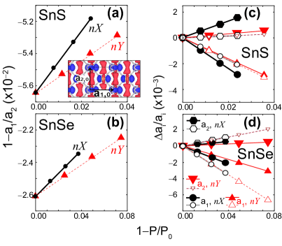
The inset in Fig. 4(a) displays the charge rearrangement upon illumination of the SnS monolayer as a charge density difference plot between the photoexcited state at k-point and the ground state, prior to any structural optimization. Red isosurfaces (with a density of electrons/Å3) indicate excess electronic charge and blue isosurfaces (with a density of electrons/Å3) show electron depletion. As indicated earlier on, charge rearrangement is bound to occur upon photoexcitation, and regardless of the numerical method employed (i.e., that in Refs. Hedin (1965); Hybertsen and Louie (1986), Ref. Ullrich (2012), or the present one Görling (1999); Martin (2004); X. Gonze et al. (2009), which permits a comparatively small time-consuming tracking of the structural distortion). Local exciton wavefunctions on GeS and GeSe shown in Ref. Gomes et al. (2016) will also necessarily perturb the initial electric dipole, and are bound to lead to a structural distortion akin to the one shown here. The point is that, although numerical estimates will naturally depend on method, the modification of the lattice structure with light is being successfully demonstrated for these compounds here.
Photoexcitation in these 2D ferroelectrics originates from an inverse piezoelectric effect Paillard et al. (2016b) as follows. In 2D, the dielectric susceptibility and the dielectric tensor (both diagonal) are related as Gomes et al. (2015); Cudazzo et al. (2011); Berkelbach et al. (2013), where is the vertical separation between (periodic) layers. This way, taking the observed change in polarization (which only occurs along the axis) and considering the point-symmetry of these compounds, lattice parameters () must evolve as Gomes et al. (2015); Nye (1985):
| (1) |
as represented by the open symbols in Figs. 4(c-d). is taken as is from Ref. Gomes et al. (2015) –and expressed in Å– and relaxed-ion values for were taken from Ref. Fei et al. (2015); is the permittivity of vacuum 111An additional factor of two multiplying arises from the length scale chosen for the vertical direction: in Ref. Fei et al. (2015), and in Ref. Gomes et al. (2015).. These predicted trends are of the same order of magnitude to the values of and determined upon a full optimization of the photoexcited structure, and they imply that photostriction is primarily produced by an inverse piezoelectric effect due to a dipole screening by the photoexcited charge carriers.
Note that the slope in Eqn. 1 is independent of the valley being photoexcited ( or ), making the predicted values for lie upon the same straight line. While we assumed in the model the same Born effective charges for the two valleys in computing , the actual polarization may be slightly different when exciting the or the valley. As shown next, an electronic/hole pressure may also produce slight differences in slope when exciting different valleys.
| SnS | SnSe | ||||||
|---|---|---|---|---|---|---|---|
| 0.029 | 0.023 | 0.023 | 0.029 | 0.027 | 0.024 | 0.024 | 0.026 |
| 0.5 |
Elongation of in-plane lattice vectors leads to positive stress. But when let to relax, the material contracts back to its original structure. In general, any structure with positive stress will contract in response. Therefore, in a first approximation, the lattice also displays an elastic response (having a negative sign) given by:
| (2) |
Using the elastic coefficients from Ref. Gomes et al. (2015), and the in-plane stress recorded in Table I for from the initial photoexcited structure prior to any structural relaxation, we obtain changes of from Eqn. (2) that are an order of magnitude smaller than those seen in Fig. 4(c-d). This way, the numerical results from the structural optimization must be dominated by the inverse piezoelectric effect, thus showing the relevance of ferroelectricity for this effect to occur in 2D materials.
The trends in Figs. 2-4 are similar to those for BiFeO3, which implies similar mechanisms at play. Experimental realization of ferroelectric 2D monochalcogenide monolayers K. Chang et al. (2016) enhances the present relevance of this work, and brings optimism in that the unique effects here described will soon be experimentally verified.
In conclusion, the SCF method has been employed to predict photostriction of a novel family of 2D ferroelectrics known as group IV monochalcogenides. Photostriction results in a decrease of the larger lattice vector and an increase of the smaller one , and it leads to a decrease of the area of the unit cell. It mainly arises from an inverse piezoelectric effect that reduces the dipole moment in the unit cell and contracts the lattice vector that is parallel to the electric dipole. The results provided in the present Letter continue to highlight unique properties of two-dimensional ferroelectrics and their potential usefulness for mechano-opto-electronic applications.
We are grateful to H. Churchill, B. Hamad and S. Sharifzadeh for discussions. R. Haleoot acknowledges funding from The Higher Committee For Education Development of Iraq. S. B.-L. was funded by an Early Career Grant from the US DOE (Grant DE-SC0016139). C.P. thanks the support from DARPA Grant No. HR0011-15-2-0038 (MATRIX program). B.X. and L.B. acknowledge the US AFOSR Grant No. FA9550-16-1-0065. Calculations were done at SDSC’s Comet (XSEDE TG-PHY090002).
References
- Tatsuzaki et al. (1966) I. Tatsuzaki, K. Itoh, S. Ueda, and Y. Shindo, Phys. Rev. Lett. 17, 198 (1966).
- V. M. Fridkin et al. (1967) V. M. Fridkin et al., Appl. Phys. Lett. 10, 354 (1967).
- Kundys (2015) B. Kundys, Appl. Phys. Rev. 2, 011301 (2015).
- Paillard et al. (2016a) C. Paillard, X. Bai, I. C. Infante, M. Guennou, G. Geneste, M. Alexe, J. Kreisel, and B. Dkhil, Adv. Mater. 28, 5153 (2016a).
- Dogan et al. (2001) A. Dogan, P. Poosanaas, I. R. Abothu, S. Komarneni, and K. Uchino, J. Ceramic Soc. Japan 109, 493 (2001).
- Kundys et al. (2010a) B. Kundys, M. Viret, D. Colson, and D. Kundys, Nat. Mater. 9, 803 (2010a).
- Kundys et al. (2012) B. Kundys, M. Viret, C. Meny, V. Da Costa, D. Colson, and B. Doudin, Phys. Rev. B 85, 092301 (2012).
- Fridkin (1979) V. Fridkin, Photoferroelectrics, 1st ed., Springer Series in Solid-State Sciences, Vol. 9 (Springer, Berlin, 1979).
- V. Iurchuk et al. (2016) V. Iurchuk et al., Phys. Rev. Lett. 117, 107403 (2016).
- Paillard et al. (2016b) C. Paillard, B. Xu, B. Dkhil, G. Geneste, and L. Bellaiche, Phys. Rev. Lett. 116, 247401 (2016b).
- Jin et al. (2012) Z. Jin, Y. Xu, Z. Zhang, X. Lin, G. Ma, Z. Cheng, and X. Wang, Appl. Phys. Lett. 101, 242902 (2012).
- D. Daranciang et al. (2012) D. Daranciang et al., Phys. Rev. Lett. 108, 087601 (2012).
- H. Wen et al. (2013) H. Wen et al., Phys. Rev. Lett. 110, 037601 (2013).
- Ruello et al. (2012) P. Ruello, T. Pezeril, S. Avanesyan, G. Vaudel, V. Gusev, I. C. Infante, and B. Dkhil, Appl. Phys. Lett. 100, 212906 (2012).
- Lejman et al. (2014) M. Lejman, G. Vaudel, I. Infante, P. Gemeiner, V. Gusev, B. Dkhil, and P. Ruello, Nat. Commun. 5, 4301 (2014).
- D. Schick et al. (2014) D. Schick et al., Phys. Rev. Lett. 112, 097602 (2014).
- Wen et al. (2015) H. Wen, M. Sassi, Z. Luo, C. Adamo, D. G. Schlom, K. M. Rosso, and X. Zhang, Sci. Rep. 5, 15098 (2015).
- Castellanos-Gomez (2016) A. Castellanos-Gomez, Nat. Photonics 10, 202 (2016).
- W. Xiaomu et al. (2015) W. Xiaomu et al., Nat. Nanotech. 10, 517 (2015).
- Basov et al. (2016) D. N. Basov, M. M. Fogler, and F. J. García de Abajo, Science 354 (2016), 10.1126/science.aag1992.
- Basov and Fogler (2016) D. N. Basov and M. M. Fogler, Nat. Nanotech. , advance online publication (2016).
- Tritsaris et al. (2013) G. A. Tritsaris, B. D. Malone, and E. Kaxiras, J. Appl. Phys. 113, 233507 (2013).
- Singh and Hennig (2014) A. K. Singh and R. G. Hennig, Appl. Phys. Lett. 105, 042103 (2014).
- Zhu et al. (2015) Z. Zhu, J. Guan, D. Liu, and D. Tománek, ACS Nano 9, 8284 (2015).
- M. Mehboudi et al. (2016) M. Mehboudi et al., Nano Lett. 16, 1704 (2016).
- K. Chang et al. (2016) K. Chang et al., Science 353, 274 (2016).
- Wu and Zeng (2016) M. Wu and X. C. Zeng, Nano Lett. 16, 3236 (2016).
- Mehboudi et al. (2016) M. Mehboudi, B. M. Fregoso, Y. Yang, W. Zhu, A. van der Zande, J. Ferrer, L. Bellaiche, P. Kumar, and S. Barraza-Lopez, Phys. Rev. Lett. 117, 246802 (2016).
- Hanakata et al. (2016) P. Z. Hanakata, A. Carvalho, D. K. Campbell, and H. S. Park, Phys. Rev. B 94, 035304 (2016).
- Fei et al. (2016) R. Fei, W. Kang, and L. Yang, Phys. Rev. Lett. 117, 097601 (2016).
- Wang and Qian (2016) H. Wang and X. Qian, arXiv:1606.04522 (2016).
- Hedin (1965) L. Hedin, Phys. Rev. 139, A796 (1965).
- Hybertsen and Louie (1986) M. S. Hybertsen and S. G. Louie, Phys. Rev. B 34, 5390 (1986).
- Ullrich (2012) C. A. Ullrich, Time-Dependent Density-Functional Theory, Concepts and Applications, 1st ed. (Oxford U. Press, N. Y., 2012).
- Kundys et al. (2010b) B. Kundys, M. Viret, D. Colson, and D. O. Kundys, Nat. Mater. 9, 803 (2010b).
- Görling (1999) A. Görling, Phys. Rev. A 59, 3359 (1999).
- Martin (2004) R. M. Martin, Electronic Structure: Basic Theory and Practical Methods, 1st ed. (Cambridge U. Press, Cambridge, UK, 2004).
- Gavnholt et al. (2008) J. Gavnholt, T. Olsen, M. Engelund, and J. Schiøtz, Phys. Rev. B 78, 075441 (2008).
- Kitaoka et al. (2013) Y. Kitaoka, K. Nakamura, T. Akiyama, T. Ito, M. Weinert, and A. J. Freeman, Phys. Rev. B 87, 205113 (2013).
- Nawa et al. (2016) K. Nawa, Y. Kitaoka, K. Nakamura, H. Imamura, T. Akiyama, T. Ito, and M. Weinert, Phys. Rev. B 94, 035136 (2016).
- X. Gonze et al. (2009) X. Gonze et al., Comp. Phys. Comm. 180, 2582 (2009).
- Blöchl (1994) P. E. Blöchl, Phys. Rev. B 50, 17953 (1994).
- Garrity et al. (2014) K. F. Garrity, J. W. Bennett, K. M. Rabe, and D. Vanderbilt, Comp. Mat. Sci. 81, 446 (2014).
- Perdew et al. (1996) J. P. Perdew, K. Burke, and M. Ernzerhof, Phys. Rev. Lett. 77, 3865 (1996).
- Gomes et al. (2016) L. C. Gomes, P. E. Trevisanutto, A. Carvalho, A. S. Rodin, and A. H. Castro Neto, Phys. Rev. B 94, 155428 (2016).
- Lui et al. (2014) C. H. Lui, A. J. Frenzel, D. V. Pilon, Y.-H. Lee, X. Ling, G. M. Akselrod, J. Kong, and N. Gedik, Phys. Rev. Lett. 113, 166801 (2014).
- Fei et al. (2015) R. Fei, W. Li, J. Li, and L. Yang, Appl. Phys. Lett. 107, 173104 (2015).
- Gomes et al. (2015) L. C. Gomes, A. Carvalho, and A. H. Castro Neto, Phys. Rev. B 92, 214103 (2015).
- Cudazzo et al. (2011) P. Cudazzo, I. V. Tokatly, and A. Rubio, Phys. Rev. B 84, 085406 (2011).
- Berkelbach et al. (2013) T. C. Berkelbach, M. S. Hybertsen, and D. R. Reichman, Phys. Rev. B 88, 045318 (2013).
- Nye (1985) J. Nye, Physical properties of crystals (Oxford U. Press, UK, 1985).
- Note (1) An additional factor of two multiplying arises from the length scale chosen for the vertical direction: in Ref. Fei et al. (2015), and in Ref. Gomes et al. (2015).