Controlling plasmon modes and damping in buckled two-dimensional material open systems
Abstract
Full ranges of both hybrid plasmon-mode dispersions and their damping are studied systematically by our recently developed mean-field theory in open systems involving a conducting substrate and a two-dimensional (2D) material with a buckled honeycomb lattice, such as silicene, germanene, and a group \@slowromancapiv@ dichalcogenide as well. In this hybrid system, the single plasmon mode for a free-standing 2D layer is split into one acoustic-like and one optical-like mode, leading to a dramatic change in the damping of plasmon modes. In comparison with gapped graphene, critical features associated with plasmon modes and damping in silicene and molybdenum disulfide are found with various spin-orbit and lattice asymmetry energy bandgaps, doping types and levels, and coupling strengths between 2D materials and the conducting substrate. The obtained damping dependence on both spin and valley degrees of freedom is expected to facilitate measuring the open-system dielectric property and the spin-orbit coupling strength of individual 2D materials. The unique linear dispersion of the acoustic-like plasmon mode introduces additional damping from the intraband particle-hole modes which is absent for a free-standing 2D material layer, and the use of molybdenum disulfide with a large bandgap simultaneously suppresses the strong damping from the interband particle-hole modes.
pacs:
71.45.Gm, 73.21.-b, 77.22.ChI Introduction
Plasmons, or self-sustained electron density oscillations, represent a broad interest and have become an important subject for both traditional and recently discovered two-dimensional (2D) materials. Stern (1967); Hwang and Das Sarma (2007); Wunsch et al. (2006); Pyatkovskiy (2008); Stauber et al. (2010); Scholz et al. (2012); Das Sarma and Li (2013); Scholz et al. (2013) Due to the possibility of fabricating complex stacking layered structures, low-dimensional materials have become very attractive for novel quantum-electronic devices. Discovery of graphene, successfully fabricated in 2004, has initiated a number of new transport and optical studies Novoselov et al. (2005); Geim and Novoselov (2007); Neto et al. (2009) due to its unusual electronic properties originating from the relativistic linear dispersion of its energy bands. In particular, graphene plasmonics has quickly become one of the actively-pursued research focuses. As an example, novel optical devices in a wide-frequency range showed significant improvement in all the crucial device characteristics (see Ref. [Politano and Chiarello, 2014] and the references therein). At high energies, the -bond plasmons in graphene demonstrate both anisotropy and splitting. Despoja et al. (2013) Moreover, a plasmonic nanoarray coupled to a single graphene sheet was found to have significant enhancements in resonant Raman scattering, as well as in spectral shifts of diffractively-coupled plasmon resonances. Plasmon resonances can be employed for investigating chemical properties of either graphene or another adjacent bulk surface, displaying the maturing capabilities of graphene-based plasmonics. Politano and Chiarello (2014); Papasimakis et al. (2010); Kravets et al. (2012); Xia et al. (2011); Yan et al. (2011) A junction between graphene and metallic contacts could also be used to design and fabricate a high-performance transistor. Consequently, exact knowledge about the plasmon dispersions and their mode damping in hybrid devices based on the newly discovered 2D materials seems absolutely necessary for the full development of these novel devices and the extension of their applications. F. H. L. Koppens et al. (2014); Han et al. (2014)
Historically, it is well known that the time evolution of a plasmon excitation in a closed system (e.g., free-standing 2D layers) is determined by two-particle Green’s functions in many-body theory, from which we are able to derive both the plasmon dispersion and the plasmon dissipation (damping) rate. Gumbs and Huang (2013) However, in an open system, Campisi et al. (2011, 2009); Esposito et al. (2009); Crooks (2008); Mukamel (2003); De Roeck and Maes (2004); Crooks (1999); Setiawan and Sarma (2015) the time evolution for electronic excitations becomes much more involved since it depends strongly on the Coulomb interaction with the environment (e.g., electron reservoirs). As an example, the classical and quantum dynamical phenomena in open systems include tunnel-coupling to external electrodes, Weiss (1999) optical-cavity leakage to free space, Illes et al. (2015) and thermal coupling to heat baths. Silaev et al. (2014) The coupling to an external reservoir is usually accompanied by extra dissipation channels. Many dynamical energy-dissipation theories for open systems are based on the so-called Lindblad dissipative superoperator. Schaller (2014)
In spite of the obvious advantages, such as being fast and tunable, in designing graphene-based devices, creating a sizable energy bandgap has become an important issue for the practical use of graphene for transistors. The reason behind this issue is electrons in gapless graphene may not be confined well by an electrostatic gate voltage or blocked by an energy barrier. Katsnelson et al. (2006); Ezawa (2012a) Scientists suggested many approaches for opening an energy gap around eV by using various insulating substrates, Giovannetti et al. (2007); Kharche and Nayak (2011); Ni et al. (2008) and graphene nanoribbons with quantized transverse wave vectors, or even by shining an intensive and polarized irradiation to dress electrons in graphene. Kibis (2010)
In this respect, experimental implementation of a 2D lattice with a sizable spin-orbit coupling seems to be an important advancement. Buckled structures, such as silicene and germanene in which atoms are displaced out of the plane due to hybridization, exhibit significant asymmetry with respect to the and sublattices. This leads to a new type of bandgap which is tunable by applying a perpendicular electric field. Physically, silicene and other buckled honeycomb lattices have been modeled successfully by introducing the Kane-Mele type Hamiltonian Kane and Mele (2005) with an intrinsic spin-orbit energy gap (meV for silicene) to low-energy electrons. Systems meeting such requirements have already been realized experimentally. Ezawa (2012a, b); Liu et al. (2011) This includes recently synthesized germanene Zhang et al. (2015); Acun et al. (2015); Li et al. (2014); Dávila et al. (2014); Bampoulis et al. (2014); Derivaz et al. (2015) with a considerably larger spin-orbit coupling and the bandgap of meV. The Hamiltonian, energy dispersion, and related electronic properties of germanene are qualitatively similar to those of silicene, although the Fermi velocity, the bandgap induced by spin-orbit coupling and the buckling height in germanene are still different in magnitudes. We, therefore, believe that our previous theory Iurov et al. ((to appear) for silicene can equally be applicable to Ge-based hybrid structures.
Germanene layers have been fabricated by molecular beam epitaxy on surfaces through deposition on h-AlN and investigated by x-ray absorption spectroscopy. d’Acapito et al. (2016) Here, h-AlN was used to create an insulating buffer layer between germanene and its metal substrate. The measured lattice constant is in good agreement with the theoretical predictions for a free-standing Ge layer. In addition, a thorough experimental study for the density of states of germanene which had been synthesized on GePt crystals at finite temperatures was performed by using a scanning-tunneling electron microscope. Walhout et al. (2016) The obtained virtually perfect linearly dependent density of states is clearly a proof of a 2D Dirac system. Furthermore, Friedel oscillations were not observed, implying the possible Klein paradox within the considered system.
Recently, there has been a number of reported studies on microscopic electronic properties, insulating regimes and topologically protected edge states within a certain range of applied electric fields, as well as spin- and valley-polarized quantum Hall effects. Aufray et al. (2010); De Padova et al. (2010); Lalmi et al. (2010); Tabert and Nicol (2013a, b, c) Here, a crucial feature for a buckled structure is the occurrence of the topological-insulator (TI) properties when the external electrostatic field is relatively low and the resulting field-related energy gap becomes less than the intrinsic spin-orbit one. If the two gaps are equal, on the other hand, the system turns into a spin-valley polarized metal (VSPM) since the gap for one of the two subbands will close. For a strong electric field, the system behaves just like a regular band insulator (BI). Tabert and Nicol (2014); Ezawa (2012a) One expects that the TI phase can show some unique electronic properties. Qi and Zhang (2011); Hasan and Kane (2010) Indeed, the properties of a TI, and the energy bandgap of Si as well, are experimentally found tunable Yan et al. (2015) by an in-plane biaxial strain.
In addition to silicene and germanene, another atomically thin 2D material with a great potential for applications in electronic devices is (monolayer molybdenum disulfide, or ML-MDS) which is a prototype of a metal dichalcogenide. The first-principle studies of the electron structure of this material has predicted a hybridization of the -orbitals of molybdenum atoms with the -orbitals of sulfur atoms, giving rise to a two-band continuum model for monolayer. Mak et al. (2010); Radisavljevic et al. (2010); Cao et al. (2012); Rostami et al. (2013) This model further indicates the existence of two spin and valley degenerate subbands with a very large direct bandgap (eV) and a strong spin-orbit interaction. Xiao et al. (2012); Scholz et al. (2013). It is important to note that the electronic properties of a ML-MDS are drastically different from its bulk samples with an indirect bandgap eV. Apart from the bandgap difference, the mobility of a single-layer at the room-temperature exceeds cm2V-1s-1 and also acquires an ultralow standby power dissipation. Together with its direct bandgap, this makes ML-MDS an excellent candidate for next generation field-effect transistors. In strong contrast to the bulk, the monolayer can emit light efficiently, and a possible high-temperature superfluidity, as a two-component Bose gas, has been predicted Berman and Kezerashvili (2016) in a system involving a transition metal dichalcogenide bilayer. Experimentally, germanene has already been successfully synthesized on substrate. Zhang et al. (2016) This leads to a huge advantage in comparison with the germanene synthesis on a metallic substrate in which germanene is strongly hybridized with metals, leading to two parabolic bands, instead of linearly dispersing bands, at its six points.
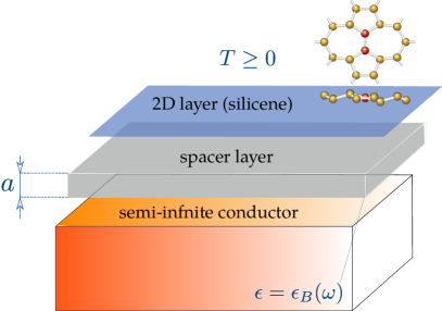
Our main focus in this paper is studying electron interactions in 2D-material open systems (2DMOS), i.e., a nanoscale hybrid structure of a 2D layer (graphene with or without energy gap, silicene, germanene, a transition-metal dichalcogenide monolayer), as illustrated by Fig. 1. The most distinguished feature of such an open system is the dynamically-screened Coulomb interaction between electrons in graphene and the conducting substrate. Gumbs et al. (2015a) Screening is included by calculating the nonlocal frequency-dependent inverse dielectric function which is related to the regular dielectric function by . The resonance occurring in corresponds to the nonlocal plasmon modes. The bare Coulomb potential in this open system would be screened, leading to . The mean-field formalism for nonlocal plasmon modes of a 2D layer interacting with a thick conductor was discussed in Refs. [Gumbs and Huang, 2013; Morgenstern Horing et al., 1985; Kouzakov and Berakdar, 2012; Horing, 2009]. This theory had given rise to a linear plasmon branch, which was later confirmed by an experiment. Kramberger et al. (2008) Similar plasmon branches were also shown for double graphene layers at different temperatures. Gumbs et al. (2015a, 2014); Iurov et al. (2016); Horing et al. (2016); Gumbs et al. (2016a) Furthermore, our previous work studied the plasmon instability in the graphene double-layer system, predicting an instability-based terahertz emission, Gumbs et al. (2015b) and nonlocal plasmons in a metal-graphene-metal encapsulated structure. Gumbs et al. (2016b)
As it was reported before Gumbs et al. (2015a) the energy gap plays a crucial role on the nonlocal collective modes since it affects both plasmon branches and Landau damping due to single-particle excitations. Pyatkovskiy (2008) Taking this into account, we focus on the effects of energy gaps and particle-hole modes (PHMs) in all three distinguishable insulating regimes of silicene, i.e., TI, VSPM and regular BI. Ezawa (2012a, b); Liu et al. (2011); Tabert and Nicol (2014) Here, both the energy gaps and PHMs could be independently tuned by applying an electric field perpendicular to the silicene layer.
The rest of the paper is organized as follows. In Sec. II, we first study nonlocal plasmon excitations in the silicene system. Our numerical results show plasmon modes and their damping as functions of frequencies and wave numbers for different parameters including Fermi energies, spin-orbit and sublattice asymmetry bandgaps, and various surface-plasmon frequencies and coupling strengths. In some limiting cases, analytical results for the plasmon modes are presented and analyzed for their dependencies on sample structure parameters. In Sec. III, we further explore the band-energy dispersions and the electronic states of molybdenum disulfide, indicating relevance to recently discovered group \@slowromancapiv@ dichalcogenides. For these materials, crucial analytical results are obtained for the wave functions, overlap factor and Fermi energy, which have not yet been addressed adequately in the literature. Additionally, we also investigate nonlocal plasmon branches in the long-wavelength limit and demonstrate how they are affected by the mismatch of and doping types and densities. Finally, concluding remarks and discussion of our numerical results in this paper are presented in Sec. IV.
II Hybrid plasmon modes and damping in open silicene systems
In this section, we discuss hybrid-plasmon dynamics in a silicene open system at low temperatures, and we will address the molybdenum-disulfide open system in the next section. For a single silicene layer, the low-energy Hamiltonian Tabert and Nicol (2014); Ezawa (2012c); Badalyan et al. (2009); Ezawa (2012a, b) at the corners of the first Brillouin zone is
| (1) |
where is the intrinsic spin-orbit energy gap, represents the field-dependent sublattice asymmetry bandgap with as an applied electric field perpendicular to the lattice, is the unit matrix, and are the Pauli matrices determining, respectively, the electron spin and valley pseudospin states of the system, labels two inequivalent and valleys, and the silicene Fermi velocity is just half of that in graphene.
This Hamiltonian in Eq. (1) can be cast into block-diagonal form with two matrices given by
| (2) |
where is the spin eigenvalue of and is the valley indices. The energy dispersions, , associated with Eq. (2) are
| (3) |
which represent a pair of spin-dependent energy subbands for each valley and have two corresponding non-equivalent bandgaps . The positive (negative) sign in Eq. (3) is for electron (hole) states. For simplicity, we, therefore, introduce the notations, and , for these two unequivalent bandgaps. The key issues in this section are obtaining spectra of hybrid-plasmon excitations in 2DMOS with new ingredients and calculating screened Coulomb couplings of electrons in silicene layers to an adjacent semi-infinite bulk plasma.
It is known that the coupling of electrons in 2D materials to other conduction electrons in 2DMOS will change the plasmon-mode dispersion. Since the damping region is still decided by the PHMs in 2D materials, this will lead to a modification to the damping of plasmon modes in 2DMOS. According to Refs. [Gumbs and Huang, 2013; Morgenstern Horing et al., 1985; Kouzakov and Berakdar, 2012; Horing, 2009], the Fourier-transformed nonlocal composite inverse dielectric function can be determined by
| (4) |
In Eq. (4), is the electron polarizability of silicene (explicitly given below), the interaction of silicene with the substrate is included in the second term, is the separation of the silicene layer from the conducting surface, and with as the average dielectric constant of silicene and spacer layer. Moreover, represents the local inverse dielectric function of the conducting substrate, expressed as
| (5) | |||||
where is a unit-step function, () corresponds to the spacer layer (conductor), separated by the surface at . We have also assumed a Drude model in Eq. (5) for the substrate dielectric function , where is the bulk-plasma frequency. Here, depends on the electron concentration , substrate dielectric constant , the effective mass of electrons, and it can vary in a very large range from ultra-violet (metals) down to infrared or even terahertz (doped semiconductors) frequencies. The use of the Drude model in Eq. (5) can be justified by a short screening length for high electron concentrations in bulk materials.
Finally, we are in a position to calculate the hybrid-plasmon modes in 2DMOS. The plasmon dispersions for a single silicene layer can be obtained from the dielectric-function equation: , where . For 2DMOS, on the other hand, should be replaced by the so-called “dispersion factor” , which appears in Eq. (4) and is calculated as
| (6) |
This verifies that the plasmon dispersions in 2DMOS will indeed be modified by coupling to other conduction electrons ().
Since the Coulomb coupling between electrons in different ( and ) valleys involves two uncompensated very large lattice wave numbers, the resulting electron interaction becomes negligible in comparison with those of electrons within the same valley. Consequently, by ignoring inter-valley Coulomb coupling and using the one-loop approximation Tabert and Nicol (2014) for silicene, we find
| (7) |
and for each subband we get
| (8) |
where denote electron and hole states, respectively, at zero temperature and is the Fermi energy of electrons in silicene.
II.1 Approximate analytical results
In the long-wavelength limit ( is the Fermi wave number for each subband), the bare bubble polarization function for is obtained as Sensarma et al. (2010)
| (9) |
where , , and is the electron areal density for each subband. Therefore, from for a single silicene layer, we get the following plasmon branch
| (10) |
where, for convenience, we introduce a coefficient .
It is important to note that the Fermi energy for silicene is fixed by the total electron areal density through
| (11) |
and if is small, we can further approximately obtain
| (12) |
This leads to . For gapped graphene, we have , and Eq. (12) gives rise to . In this case, we get and from Eq. (10) we find . Actually, such a scaling relation holds true for all 2D materials except for gapless graphene which yields . Additionally, in contrast to Eq. (10), if with an unoccupied upper subband, we obtain the plasmon mode
| (13) |
In the above discussion, we are only restricted to the plasmon mode for a stand-alone silicene. For the 2DMOS, on the other hand, when both subbands are occupied, the plasmon modes are determined by Eqs. (6) and (9), yielding
| (14) |
which gives rise to the following bi-quadratic equation
| (15) |
Its two solutions are simply given by
| (16) |
where the sign () corresponds to the in-phase (out-of-phase) plasmon mode. For the strong-coupling regime with and in the long-wavelength limit, the split hybrid plasmon modes are found to be
| (17) |
In Eq. (17), the linear dispersions and their prefactor scalings are the same as those for graphene. Gumbs et al. (2015a) However, the two independent bandgaps, and , play unique roles in shaping the hybrid-plasmon branches when the damping from different PHMs is considered. It is found that the outer PHM’s boundaries are only determined by and the two hybrid-plasmon group velocities (slopes) are proportional to and . These two group velocities drop to zero as and increase since for low doping. If a proper applied electric field is chosen, the VSPM phase can be reached with . For , on the other hand, we know the plasmon frequencies for both gapped graphene Pyatkovskiy (2008) and silicene Tabert and Nicol (2014) are reduced by finite . Meanwhile, these plasmon branches will enter into a gap region between the interband and intraband PHMs. As a result, we find that both the damping-free plasmon regions and the plasmon group velocities can be controlled independently by and . This requirement can be fulfilled by scanning an external electric field, even for a fixed spin-orbit interaction strength, leading to distinctive behaviors for TI and BI phases.
Moreover, the plasmon group velocity associated with the mode in 2DMOS depends on in the strong-coupling regime. However, in the weak-coupling regime with , this plasmon mode becomes proportional to , as shown in Eq. (10) for a single silicene layer. Meanwhile, the plasmon group velocity for the mode, which is independent of , approaches zero in the weak-coupling regime.
II.2 Full numerical solutions
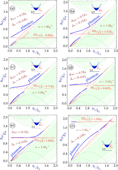
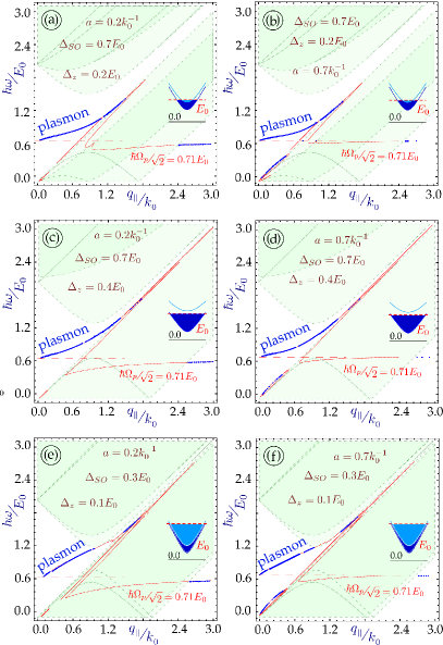
For our numerical results presented in Figs. 2-6, we use the scale for the energy and the scale for the wave number , where , with as the total doped electron areal density. Here, the constant value cm-2 is given for these five figures.
The features of the hybrid plasmon modes beyond the long-wavelength limit could be explored numerically for all possible values of the energy bandgaps based on the exact calculation of the polarization function for a silicene layer Tabert and Nicol (2014) and the use of Eq. (6). Here, two subbands can be selectively populated by controlling or . Furthermore, the coupling of electrons to the surface of a semi-infinite conductor in 2DMOS can also be tuned by choosing the separation of the silicene layer from the bulk surface.
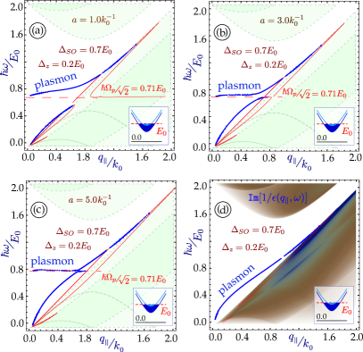
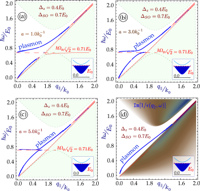
We first consider a case with a relatively large minimal bandgap and both subbands occupied. The numerical results for this case are presented in Fig. 2, where both the dispersion and undamped extension of the lower acoustic-like branch mainly depend on the separation . The anticrossing of two hybrid plasmon modes can be seen most clearly in Fig. 2() with . In comparison with the plasmon damping for free-standing slicene in Fig. 2(), the upper optical-like branch is free from damping into the main diagonal (, intraband PHM) until exceeding a relatively large critical wave number, as shown in Figs. 2()-2(). For in Fig. 3, where only the lower subband is occupied, the plasmon-mode dispersions are found to be similar to gapped graphene in Ref. [Gumbs et al., 2015a]. For in Fig. 3(), the anticrossing feature becomes almost indistinguishable, and the lower branch approaches that of free-standing slicene in Fig. 3().
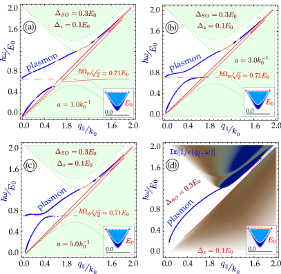
The situation with an even smaller bandgap and two occupied subbands is presented in Fig. 4. Here, we find an unusual feature that the upper branch damps into both intraband and interband PHM regions at different wave numbers. For a free-standing silicene sample in Fig. 4(), however, the damping always occurs at one of the PHM boundaries, and the increase of bandgap makes it more favorable for the plasmon-mode damping to occur at the interband PHM region. In addition, we also find that the anticrossing feature becomes more significant in the weak-coupling regime, as displayed in Fig. 4().
It is known that the external parameter in the 2DMOS, i.e., the plasma frequency , can greatly affect the damping of the hybrid plasmon modes. Our results for different values of are shown in Fig. 5. It is very surprising to see from Figs. 5()-5() that the damping-free range of the lower branch will depend on but not on the other internal parameters, such as , and . From Fig. 5(), on the other hand, we observe that the upper branch could be doubly damped by both intraband and interband PHM regions, which also exists for a gapped graphene open system.
It is reasonable to expect that the open-system damping effect will become more significant if the conductor surface stays closer to the silicene layer. The numerical results for the plasmon dispersions with much smaller separations are presented in Fig. 6, from which we reproduce a recent experimentally confirmed effect in graphene, Politano et al. (2011, 2012); Politano and Chiarello (2013); Horing et al. (2016) i.e., the acoustic-like plasmon branch will be highly damped in the long-wavelength limit as nm. This damping effect can be found for all considered cases in Figs. 6()-6() with various energy gaps. It is interesting to note from Fig. 6 that the group velocity of the upper branch almost does not depend on the separation , but strongly depends on the energy gap .
III Hybrid plasmon modes and damping in open molybdenum-disulfide systems
The two-band model Hamiltonian for molybdenum disulfide, as well as for most other transition-metal dichalcogenides, next to the two inequivalent and valley points can be written as Xiao et al. (2012); Scholz et al. (2013)
| (18) |
where and are the valley and spin indices, eV is the main energy bandgap, is the spin-orbit coupling parameter, represents the free electron mass, are the Pauli matrices for valley pseudospins, is the electron hopping parameter, and Å which is obtained from the MoS atom-atom bond length Å. Even though , the spin-orbit interaction is not negligible, which is reflected in the spin-resolved energy subbands and in the absence of spin degeneracy. In Eq. (18), we use and we find that Jm plays a role of the Fermi velocity and is equal to of the factor for graphene. Moreover, we neglect the trigonal warping term , which leads to the slight anisotropy of the energy for our whole study since eV does not represent a considerable effect on the electronic states. Consequently, the considered hybrid plasmon are also isotropic.
It is easy to verify that the Hamiltonian in Eq. (18) is equivalent to that of gapped graphene with a dependent “gap” term, , as well as a dependent band-shift term, , yielding
| (19) |
where determines the electron or hole state in complete analogy to graphene with or without a gap. By neglecting all the higher-order terms on order of for small values, Eq. (19) turns into
| (20) |
Besides the simple plane-wave part, the spinor parts of the wave functions associated with the eigenvalues in Eq. (20) for each valley are given by
| (21) |
where , , and the overlap factor is calculated as
| (22) |
Here, each part of the expression in Eq. (22) could be calculated explicitly, e.g.,
| (23) |
If we introduce the notation for a composite index and neglect the small and terms in Eq. (20), this gives rise to , and therefore, the wave function in Eq. (21) could be simplified as
| (24) |
where . It is clear from Eq. (24) that, unlike gapped graphene, two spinor components become inequivalent and their ratio is different for electron and hole states.
Furthermore, the density of states can be formally written as
| (25) |
By denoting , , , and , Eq. (20) is further simplified to . Therefore, if , from Eq. (25) we obtain the analytical result for , given by
| (26) |
where is a unit-step function, and the energy-dependent function is defined as
| (27) |
If , on the other hand, we simply find
| (28) |
Using the result in Eq. (26), all previously known cases, including a pair of parabolic bands or Dirac cones, as well as a pair of gapped Dirac cones, could be easily verified.
If we neglect the and terms in Eq. (20), i.e., setting and , we obtain from Eq. (28) the result for a pair of non-degenerate, spin- and valley-dependent subbands in gapped graphene, given by
| (29) |
It is clear from Eqs. (26), (28) and (29) that the boundaries for non-zero density of states in all three cases are set by for electrons () and for holes ().
For weak hopping with , using Eq. (20) we arrive at
| (30) |
where we have used the fact that . This result leads to the density of states given by
| (31) |
where there exist two energy-independent giant discontinuities for electrons and holes, respectively.
For electrons with at , we get the jump in the density of states given by
| (32) |
Similarly, for holes with at , we obtain two discontinuities at different energies, i.e.,
| (33) |
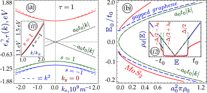
Our above analytical expressions match exactly the numerical results reported in Ref. [Scholz et al., 2013]. We note that the simplified parabolic dispersions in Eq. (30) catch the difference in electron and hole effective masses for various spin and valley indices even for . For large values, this difference becomes more significant. The numerically-calculated energy dispersions for electrons and holes and their zero-temperature Fermi energies for fixed doping density are presented in Fig. 7. It is interesting to note that at a finite energy away from the bandedge, the density of states for is significantly smaller compared to graphene. This agrees with the well-known fact that non-parabolicity in graphene energy subbands will enhance the density of states.
Now, let us turn to studies of nonlocal plasmon dispersions and their damping in a layer interacting with a semi-infinite conductor. For this case, the one-loop electron polarization function for molybdenum disulfide with two pairs of energy subbands can be obtained in a way similar to Eq. (7) by summing over a composite index for each subband but specifying values for and doping separately. We will further assume that only the lowest hole subband with will be occupied, and two electron subbands become nearly degenerate with each other since .
In the long-wavelength limit, by using Eq. (9) the polarization function of a monolayer interacting with a semi-infinite conductor separated by a distance can be expressed as
| (34) |
where is the areal density for doping, is the fine-structure constant, is the dielectric constant for , and
| (35) |
Here, the inclusion of the coupling between and the semi-infinite conductor has split plasmons into in-phase () and out-of-phase () modes in Eq. (34). This will certainly lead to a modification of plasmon-mode damping by PHMs.
The main advantage for using in a hybrid plasmonic device is its large energy gap , which allows one to consider clean metals with an extremely high plasma frequency . This arrangement is not possible for gapped graphene or silicene since the plasmon modes at such a frequency would be strongly damped by the interband PHMs. Another unique feature for is the large difference between the electron and hole doping processes, i.e., high doping density cm-2 only allows the occupation of one hole subband, as assumed in Eq.(34) for . Here, even in the parabolic approximation, the results for and doping still vary drastically. Although the correction to is very small, the density of states of electrons is almost twice as large as that of holes.
In order to determine Landau damping of the plasmon modes, we need to determine the boundaries for PHMs, defined by
| (36) |
which corresponds to . Here, is the electron Fermi wave number. For moderate doping (), from Eq. (20) its PHM boundary is found to be
| (37) |
In the long-wavelength limit with , we can approximate Eq. (37) by
| (38) |
where we use the facts that and and is determined by .
Alternatively, if the sample is doped (), the PHM boundaries with for the occupied hole subband is found to be
| (39) |
These two PHM boundaries, , determine whether the acoustic-like plasmon branch would be Landau damped or not. On the other hand, the optical-like plasmon branch originating from is considered to be far away from the interband PHM boundary starting around eV.
IV Summary and concluding remarks
In conclusion, we have presented in this paper the numerical results for full ranges of hybrid plasmon-mode dispersions, as well as analytical expressions in the long-wavelength limit, in an open interacting system including a 2D material and a conducting substrate. Although the plasmon damping is set by the particle-hole modes(PHMs) of electrons in the 2D material, the strong coupling between electrons in 2D materials and in the conducting substrate gives rise to a splitting of plasmons into one in-phase and one out-of-phase mode. Such dramatic changes in plasmon dispersions are expected to have impacts on the damping of these modes. In addition, in comparison with gapped graphene, the different plasmon modes in silicene or transition-metal dichalcogenides make our damping studies even more distinctive, including different energy bandgaps, doping types, occupations of subbands, and coupling between 2D materials and the conducting substrate. Here, each plasmon branch and its damping can be independently analyzed based on the signatures of the PHMs since the plasmon modes depend on both spin and valley degrees of freedom. Therefore, our proposed hybrid systems in this paper are expected to be useful in measuring the dielectric property of 2D material open systems (2DMOS) and spin-orbit coupling strength of individual 2D materials. More importantly, we have demonstrated the possibility to design the plasmonic resonances at almost all frequencies and wave numbers for different types of newly discovered 2D materials. This was not feasible for either a free-standing silicene layer or a graphene-based hybrid structure.
Additionally, our model and numerical results for 2DMOS have confirmed a recently discovered phenomenon related to a significant damping of an acoustic-like plasmon branch as the separation to the conducting substrate becomes very small. From our current studies, we have found that in silicene this critical distance can be modified by either applying an external electric field or varying doping types and levels. The unique linear dispersion obtained under the long-wavelength limit makes the damping from intraband PHMs possible in 2DMOS but not for a free-standing 2D layer. We have also noted that the plasma energies in clean metals are usually much larger than the Fermi energies and bandgaps in graphene. As a result, the plasmon modes in graphene can not be coupled to surface plasmons in the presence of a metallic substrate without suffering from the strong damping by interband PHMs. However, the use of with a large bandgap in 2DMOS is able to suppress this damping effectively. Alternatively, one could also use Bi2Se3 material, Politano et al. (2015) which is a doped topological insulator with a surface-plasmon energy around meV, or a highly-doped semiconductor in 2DMOS.
Acknowledgements.
D.H. would like to thank the support from the Air Force Office of Scientific Research (AFOSR). We would like to mention a great help from Joseph Sadler and especially Patrick Helles, IT managers at the Center for High Technology Materials of the University of New Mexico, much beyond their official responsibilities.References
- Stern (1967) F. Stern, Phys. Rev. Lett. 18, 546 (1967).
- Hwang and Das Sarma (2007) E. H. Hwang and S. Das Sarma, Phys. Rev. B 75, 205418 (2007).
- Wunsch et al. (2006) B. Wunsch, T. Stauber, F. Sols, and F. Guinea, New Journal of Physics 8, 318 (2006).
- Pyatkovskiy (2008) P. Pyatkovskiy, Journal of Physics: Condensed Matter 21, 025506 (2008).
- Stauber et al. (2010) T. Stauber, J. Schliemann, and N. M. R. Peres, Phys. Rev. B 81, 085409 (2010).
- Scholz et al. (2012) A. Scholz, T. Stauber, and J. Schliemann, Phys. Rev. B 86, 195424 (2012).
- Das Sarma and Li (2013) S. Das Sarma and Q. Li, Phys. Rev. B 87, 235418 (2013).
- Scholz et al. (2013) A. Scholz, T. Stauber, and J. Schliemann, Phys. Rev. B 88, 035135 (2013).
- Novoselov et al. (2005) K. Novoselov, A. K. Geim, S. Morozov, D. Jiang, M. Katsnelson, I. Grigorieva, S. Dubonos, and A. Firsov, Nature 438, 197 (2005).
- Geim and Novoselov (2007) A. K. Geim and K. S. Novoselov, Nature Materials 6, 183 (2007).
- Neto et al. (2009) A. C. Neto, F. Guinea, N. Peres, K. S. Novoselov, and A. K. Geim, Reviews of Modern Physics 81, 109 (2009).
- Politano and Chiarello (2014) A. Politano and G. Chiarello, Nanoscale 6, 10927 (2014).
- Despoja et al. (2013) V. Despoja, D. Novko, K. Dekanić, M. Šunjić, and L. Marušić, Phys. Rev. B 87, 075447 (2013).
- Papasimakis et al. (2010) N. Papasimakis, Z. Luo, Z. X. Shen, F. D. Angelis, E. D. Fabrizio, A. E. Nikolaenko, and N. I. Zheludev, Opt. Express 18, 8353 (2010).
- Kravets et al. (2012) V. G. Kravets, F. Schedin, R. Jalil, L. Britnell, K. S. Novoselov, and A. N. Grigorenko, Journal of Physical Chemistry C 116, 3882 (2012).
- Xia et al. (2011) F. Xia, V. Perebeinos, Y.-m. Lin, Y. Wu, and P. Avouris, Nature nanotechnology 6, 179 (2011).
- Yan et al. (2011) J. Yan, K. S. Thygesen, and K. W. Jacobsen, Physical review letters 106, 146803 (2011).
- F. H. L. Koppens et al. (2014) F. H. L. F. H. L. Koppens, T. Mueller, P. Avouris, A. C. Ferrari, M. S. Vitiello, and M. Polini, Nature Nanotechnology 9, 780 (2014).
- Han et al. (2014) W. Han, R. K. Kawakami, M. Gmitra, and F. J., Nature Nanotechnology 9, 794 (2014).
- Gumbs and Huang (2013) G. Gumbs and D. Huang, Properties of Interacting Low-Dimensional Systems (John Wiley & Sons, 2013).
- Campisi et al. (2011) M. Campisi, P. Hänggi, and P. Talkner, Rev. Mod. Phys. 83, 771 (2011).
- Campisi et al. (2009) M. Campisi, P. Talkner, and P. Hänggi, Phys. Rev. Lett. 102, 210401 (2009).
- Esposito et al. (2009) M. Esposito, U. Harbola, and S. Mukamel, Rev. Mod. Phys. 81, 1665 (2009).
- Crooks (2008) G. E. Crooks, Journal of Statistical Mechanics: Theory and Experiment 2008, 10023 (2008).
- Mukamel (2003) S. Mukamel, Phys. Rev. Lett. 90, 170604 (2003).
- De Roeck and Maes (2004) W. De Roeck and C. Maes, Phys. Rev. E 69, 026115 (2004).
- Crooks (1999) G. E. Crooks, Phys. Rev. E 60, 2721 (1999).
- Setiawan and Sarma (2015) F. Setiawan and S. D. Sarma, arXiv preprint arXiv:1509.05067 (2015).
- Weiss (1999) U. Weiss, Quantum dissipative systems, vol. 10 (World Scientific, 1999).
- Illes et al. (2015) E. Illes, C. Roy, and S. Hughes, Optica 2, 689 (2015).
- Silaev et al. (2014) M. Silaev, T. T. Heikkilä, and P. Virtanen, Phys. Rev. E 90, 022103 (2014).
- Schaller (2014) G. Schaller, Open Quantum Systems Far from Equilibrium (Springer, Lecture Notes in Physics, 2014).
- Katsnelson et al. (2006) M. Katsnelson, K. Novoselov, and A. Geim, Nature Physics 2, 620 (2006).
- Ezawa (2012a) M. Ezawa, New Journal of Physics 14, 033003 (2012a).
- Giovannetti et al. (2007) G. Giovannetti, P. A. Khomyakov, G. Brocks, P. J. Kelly, and J. van den Brink, Physical Review B 76, 073103 (2007).
- Kharche and Nayak (2011) N. Kharche and S. K. Nayak, Nano Letters 11, 5274 (2011).
- Ni et al. (2008) Z. H. Ni, T. Yu, Y. H. Lu, Y. Y. Wang, Y. P. Feng, and Z. X. Shen, ACS Nano 2, 2301 (2008).
- Kibis (2010) O. Kibis, Physical Review B 81, 165433 (2010).
- Kane and Mele (2005) C. L. Kane and E. J. Mele, Phys. Rev. Lett. 95, 226801 (2005).
- Ezawa (2012b) M. Ezawa, Phys. Rev. Lett. 109, 055502 (2012b).
- Liu et al. (2011) C.-C. Liu, W. Feng, and Y. Yao, Phys. Rev. Lett. 107, 076802 (2011).
- Zhang et al. (2015) L. Zhang, P. Bampoulis, A. van Houselt, and H. Zandvliet, Applied Physics Letters 107, 111605 (2015).
- Acun et al. (2015) A. Acun, L. Zhang, P. Bampoulis, M. Farmanbar, A. van Houselt, A. Rudenko, M. Lingenfelder, G. Brocks, B. Poelsema, M. Katsnelson, et al., Journal of Physics: Condensed Matter 27, 443002 (2015).
- Li et al. (2014) L. Li, S.-z. Lu, J. Pan, Z. Qin, Y.-q. Wang, Y. Wang, G.-y. Cao, S. Du, and H.-J. Gao, Advanced Materials 26, 4820 (2014).
- Dávila et al. (2014) M. Dávila, L. Xian, S. Cahangirov, A. Rubio, and G. Le Lay, New Journal of Physics 16, 095002 (2014).
- Bampoulis et al. (2014) P. Bampoulis, L. Zhang, A. Safaei, R. Van Gastel, B. Poelsema, and H. J. W. Zandvliet, Journal of Physics: Condensed matter 26, 442001 (2014).
- Derivaz et al. (2015) M. Derivaz, D. Dentel, R. Stephan, M.-C. Hanf, A. Mehdaoui, P. Sonnet, and C. Pirri, Nano Letters 15, 2510 (2015).
- Iurov et al. ((to appear) A. Iurov, G. Gumbs, and D. H. Huang, Journal of Physics: Condensed Matter ((to appear)).
- d’Acapito et al. (2016) F. d’Acapito, S. Torrengo, E. Xenogiannopoulou, P. Tsipas, J. M. Velasco, D. Tsoutsou, and A. Dimoulas, Journal of Physics: Condensed Matter 28, 045002 (2016).
- Walhout et al. (2016) C. J. Walhout, A. Acun, L. Zhang, M. Ezawa, and H. J. W. Zandvliet, Journal of Physics: Condensed Matter 28, 284006 (2016).
- Aufray et al. (2010) B. Aufray, A. Kara, S. Vizzini, H. Oughaddou, C. Leandri, B. Ealet, and G. Le Lay, Applied Physics Letters 96, 183102 (2010).
- De Padova et al. (2010) P. De Padova, C. Quaresima, C. Ottaviani, P. M. Sheverdyaeva, P. Moras, C. Carbone, D. Topwal, B. Olivieri, A. Kara, H. Oughaddou, et al., Applied Physics Letters 96, 261905 (2010).
- Lalmi et al. (2010) B. Lalmi, H. Oughaddou, H. Enriquez, A. Kara, S. Vizzini, B. Ealet, and B. Aufray, Applied Physics Letters 97, 223109 (2010).
- Tabert and Nicol (2013a) C. J. Tabert and E. J. Nicol, Physical Review Letters 110, 197402 (2013a).
- Tabert and Nicol (2013b) C. J. Tabert and E. J. Nicol, Physical Review B 87, 235426 (2013b).
- Tabert and Nicol (2013c) C. J. Tabert and E. J. Nicol, Physical Review B 88, 085434 (2013c).
- Tabert and Nicol (2014) C. J. Tabert and E. J. Nicol, Phys. Rev. B 89, 195410 (2014).
- Qi and Zhang (2011) X.-L. Qi and S.-C. Zhang, Rev. Mod. Phys. 83, 1057 (2011).
- Hasan and Kane (2010) M. Z. Hasan and C. L. Kane, Rev. Mod. Phys. 82, 3045 (2010).
- Yan et al. (2015) J.-A. Yan, M. A. D. Cruz, S. Barraza-Lopez, and L. Yang, Applied Physics Letters 106, 183107 (2015).
- Mak et al. (2010) K. F. Mak, C. Lee, J. Hone, J. Shan, and T. F. Heinz, Phys. Rev. Lett. 105, 136805 (2010).
- Radisavljevic et al. (2010) B. Radisavljevic, A. Radenovic, J. Brivio, V. Giacometti, and A. Kis, Nature Nanotechnology 6, 147–150 (2010).
- Cao et al. (2012) T. Cao, G. Wang, W. Han, H. Ye, C. Zhu, J. Shi, and E. W. B. L. . J. F. Qian Niu, Pingheng Tan, Nature Communications 3, 887 (2012).
- Rostami et al. (2013) H. Rostami, A. G. Moghaddam, and R. Asgari, Phys. Rev. B 88, 085440 (2013).
- Xiao et al. (2012) D. Xiao, G.-B. Liu, W. Feng, X. Xu, and W. Yao, Phys. Rev. Lett. 108, 196802 (2012).
- Berman and Kezerashvili (2016) O. L. Berman and R. Y. Kezerashvili, Phys. Rev. B 93, 245410 (2016).
- Zhang et al. (2016) L. Zhang, P. Bampoulis, A. N. Rudenko, Q. Yao, A. van Houselt, B. Poelsema, M. I. Katsnelson, and H. J. W. Zandvliet, Physical Review Letters 116, 256804 (2016).
- Gumbs et al. (2015a) G. Gumbs, A. Iurov, and N. J. M. Horing, Phys. Rev. B 91, 235416 (2015a).
- Morgenstern Horing et al. (1985) N. J. Morgenstern Horing, E. Kamen, and H.-L. Cui, Phys. Rev. B 32, 2184 (1985).
- Kouzakov and Berakdar (2012) K. A. Kouzakov and J. Berakdar, Phys. Rev. A 85, 022901 (2012).
- Horing (2009) N. J. M. Horing, Phys. Rev. B 80, 193401 (2009).
- Kramberger et al. (2008) C. Kramberger, R. Hambach, C. Giorgetti, M. H. Rümmeli, M. Knupfer, J. Fink, B. Büchner, L. Reining, E. Einarsson, S. Maruyama, et al., Phys. Rev. Lett. 100, 196803 (2008).
- Gumbs et al. (2014) G. Gumbs, A. Iurov, and D. Huang, Coherent Phenomena 3, 1 (2014).
- Iurov et al. (2016) A. Iurov, G. Gumbs, D. Huang, and V. Silkin, Physical Review B 93, 035404 (2016).
- Horing et al. (2016) N. J. Horing, A. Iurov, G. Gumbs, A. Politano, and G. Chiarello, in Low-Dimensional and Nanostructured Materials and Devices (Springer, 2016), pp. 205–237.
- Gumbs et al. (2016a) G. Gumbs, A. Iurov, J.-Y. Wu, M. Lin, and P. Fekete, Scientific Reports 6 (2016a).
- Gumbs et al. (2015b) G. Gumbs, A. Iurov, D. Huang, and W. Pan, Journal of Applied Physics 118, 054303 (2015b).
- Gumbs et al. (2016b) G. Gumbs, N. Horing, A. Iurov, and D. Dahal, Journal of Physics D: Applied Physics 49, 225101 (2016b).
- Ezawa (2012c) M. Ezawa, Phys. Rev. B 86, 161407 (2012c).
- Badalyan et al. (2009) S. M. Badalyan, A. Matos-Abiague, G. Vignale, and J. Fabian, Phys. Rev. B 79, 205305 (2009).
- Sensarma et al. (2010) R. Sensarma, E. H. Hwang, and S. Das Sarma, Phys. Rev. B 82, 195428 (2010).
- Politano et al. (2011) A. Politano, A. R. Marino, V. Formoso, D. Farías, R. Miranda, and G. Chiarello, Phys. Rev. B 84, 033401 (2011).
- Politano et al. (2012) A. Politano, A. R. Marino, and G. Chiarello, Phys. Rev. B 86, 085420 (2012).
- Politano and Chiarello (2013) A. Politano and G. Chiarello, Applied Physics Letters 102, 201608 (2013).
- Politano et al. (2015) A. Politano, V. M. Silkin, I. A. Nechaev, M. S. Vitiello, L. Viti, Z. S. Aliev, M. B. Babanly, G. Chiarello, P. M. Echenique, and E. V. Chulkov, Phys. Rev. Lett. 115, 216802 (2015).