Study of 0- phase transition in hybrid superconductor-InSb nanowire quantum dot devices
Abstract
Hybrid superconductor-semiconducting nanowire devices provide an ideal platform to investigating novel intragap bound states, such as the Andreev bound states (ABSs), Yu-Shiba-Rusinov (YSR) states, and the Majorana bound states. The competition between Kondo correlations and superconductivity in Josephson quantum dot (QD) devices results in two different ground states and the occurrence of a 0- quantum phase transition. Here we report on transport measurements on hybrid superconductor-InSb nanowire QD devices with different device geometries. We demonstrate a realization of continuous gate-tunable ABSs with both 0-type levels and -type levels. This allow us to manipulate the transition between 0 and junction and explore charge transport and spectrum in the vicinity of the quantum phase transition regime. Furthermore, we find a coexistence of 0-type ABS and -type ABS in the same charge state. By measuring temperature and magnetic field evolution of the ABSs, the different natures of the two sets of ABSs are verified, being consistent with the scenario of phase transition between the singlet and doublet ground state. Our study provides insights into Andreev transport properties of hybrid superconductor-QD devices and sheds light on the crossover behavior of the subgap spectrum in the vicinity of 0- transition.
I. INTRODUCTION
In hybrid structures where a superconductor (S) is connected to a mesoscopic normal conductor (N), an electron in the normal region is converted to a Cooper pair into the superconductor with the reflection of a hole. This well established mechanism, known as the Andreev reflections, plays a central role in the proximity effect in which the electron pairing potential in S can penetrate into N region. During the past years, based on the idea of introducing superconducting order into low-dimensional semiconductors via the proximity effect, superconducting leads coupled semiconductor quantum dots (QDs) have been extensively investigated for novel quantum phenomena and new device conceptsSchoNN , such as tunable Josephson junctionsDoh ; Jarillo ; Xiang ; Cleuziou ; Nilsson and Cooper-pair splittersHofstetter ; StrunkCPS ; MotyCPS ; DeaconCPS , and such hybrid S-QD structures provide an ideal platform to study basic physical issues including the formation of Andreev Bound StatesBauer ; Deacon ; Pillet ; PilletB ; Simon ; Ingap , the interplay between the Kondo effect and the proximity induced superconductivityRozhkov ; LevyPi ; Egger ; Belzig ; Choi ; Buitelaar ; Tarucha07 ; Eichler07 ; Jespersen07 ; silvanoPRL ; Kim ; Kanai10 , as well as the search for Majorana fermions in solid stateLutchyn ; Oreg . Andreev Bound States (ABS), originating from the superposition of coherent Andreev reflection processes, have been attracting growing interests owing to its fundamental importance in mesoscopic superconductor related systems, and have been observed in both S-QD-S Pillet ; PilletB and S-QD-NDeacon ; Willy ; silvanoNN systems in the tunneling regime. In superconducting leads coupled QDs, the spectrum of ABSs can be dramatically influenced by Coulomb interaction and spin-related many-body Kondo correlation. Depending on the ratio of the corresponding energy scales where is the Kondo temperature and is the superconducting gap, a 0- Josephson junction transition has been predicted theoreticallyRozhkov ; Ingap ; Simon and observed experimentally by either the sign change of the Josephson supercurrentReversal ; Jorgensen ; Eichler09 ; Squid or the crossing behavior of the ABSsDeacon ; Kim ; silvanoNN . When , the Kondo screening is suppressed due to the lack of quasiparticle DOS around the Fermi level, hence the junction is in a state with a crossing of the two Andreev levels. For , a Kondo singlet forms by breaking cooper pairs at the Fermi level, thus the junction is in a 0 state and the two Andreev levels never cross. Since these two magnetic states - a doublet for the state and a singlet for the 0 state - are two different ground states (GSs) of the QD with different spins, a quantum phase transition is expected to be induced by a change of parameters in the QD device, such as the chemical potential and the charging energy.
InSb NWs own a giant g factorGiant and strong spin-orbit interaction strengthGiant ; NadjSOI ; Fan . Hybrid superconductor-InSb NW devices are expected to exhibit rich physics of subgap states due to the influence of strong spin-orbit coupling and Zeeman splitting in the presence of magnetic fields. Recently, zero-energy states have been observed in hybrid superconductor-InSb NW devices and been interpreted as Majorana Bound StatesMourik ; Mingtang ; Mingtang1 , though under certain circumstances ABSs could behave as imitations of Majorana zero-energy states, yet having no relations with topological superconducting phases. Therefore to clarify the mechanism of these subgap bound states in such systems, a systematic study of the ABSs in hybrid superconductor-InSb NWQD devices is of fundamental importance, and is still lacking.
In this work we report an extensive study on the low-temperature transport measurements of hybrid superconductor-InSb NWQD devices with different device geometries, i.e. the InSb nanowire QD(NWQD)-SQUID device and the S-NWQD-S device. In the NWQD-SQUID device we observe continuous gate-tuned ABSs with both 0-type levels and -type levels and study the evolution of the ABSs as a function of temperature, showing a tunneling transport mechanism assisted by the thermally populated ABSs. In the S-NWQD-S device, we demonstrate that two sets of 0-type and -type ABSs overlap at the same Kondo region, though a doublet ground state is favored given the estimated Kondo temperature. We propose a possible scenario for the simultaneous emergence of the 0-type and -type ABSs and this scenario can be supported by the temperature and magnetic field evolution of the ABSs.
II. EXPERIMENTAL DETAILS
The hybrid superconductor-InSb nanowire QD devices are fabricated from individual InSb segments of InAs/InSb heterostructure NWs grown on an InP substrate by MBE methodXuNanotech2012 ; Thelander2012 , with typical diameters ranging from 60 to 120 nm. After growth, the NWs are transferred onto a degenerately doped, n-type Si substrate (used as a global backgate), covered by a 110-nm thick thermal oxide. The superconducting electrodes (5 nm/100 nm Ti/Al bilayer) are fabricated using standard e-beam lithography and e-beam evaporation procedure. Before the metal deposition, the samples are etched in a diluted solution to remove the native oxide layer. The Ti layer is used as an adhesion layer between the superconducting Al layer and the nanowire. All measurements are performed in a 3He/4He dilution refrigerator with a base temperature of mK. In order to minimize the electronic noise, we used a series of -filters, copper-powder filter and RC filters thermalizing at different temperature stages The magnetic field is perpendicularly applied to the sample plane.
III. ANDREEV BOUND STATES IN NWQD-SQUID DEVICES
A. Gate-tuned different types of ABSs in NWQD-SQUID devices.
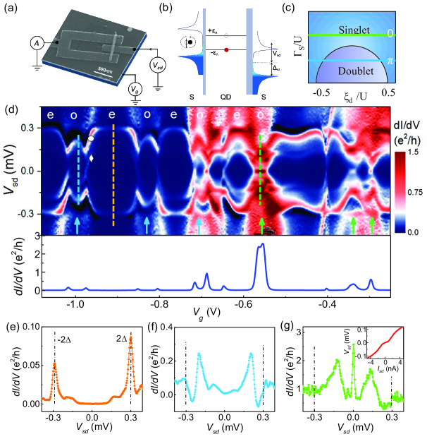
Fig. 1(a) shows a scanning electron microscope (SEM) picture of a typical InSb NWQD-SQUID device and a schematic of the measurement circuit. This geometry is commonly used to improve the energy resolution for probing subgap resonances of the QDs due to the sharp change in BCS density of states at the superconducting gap edgesPillet ; PilletB ; Willy ; Kumar ; silvanoPRL . In our case, as can be deduced from the Coulomb diamond (see section I of supplementary material), the central electrode is weakly coupled to the nanowire and plays the role of probing the DOS of levels in the nanowire. The top panel of Fig. 1(d) shows the differential conductance in the superconducting state as a function of bias voltage and backgate voltage , acquired at base temperature and zero magnetic field. We can clearly see two main features over the entire range: a pair of main resonances at higher bias voltages with high conductance () and a pair of weak resonances with low conductance () lying parallel to the main resonance. We attribute the main resonances to the alignment of the ABS levels at with the singularity in the BCS density of states of quasiparticles, i.e. at bias voltages: (see Fig. 1(b)). The weak resonances can be interpreted as a replica of the main ABSs when the residual quasiparticle DOS of the probe at the Fermi level is aligned with the ABS levels: Kumar .
In particular, we can readily identify distinct gate voltage evolution of the ABSs resonances in charge states of different parity determined by alternate size of the Coulomb diamond patterns. In regions with even electron occupation, the main ABSs resonances appear to overlap with the elastic quasiparticle cotunneling at eV, showing little dependence on gate voltage. This denotes that the ABSs are pushed towards the superconductor gap edge in the even states. Fig. 1(e) shows a trace taken at the center of the even valley indicated by the orange dashed line in Fig. 1(d). The positions of peaks in indicate the superconducting gap, eV, which correspond with a critical temperature of K. In contrast, in the odd charge states, the shape of ABSs peaks is evidently dependent on the gate voltage and shows either crossing (blue arrow) or noncrossing (green arrow) behavior within different odd-occupied Coulomb valleys. Fig. 1(f) shows a trace taken at the center of the odd valley indicated by the light-blue dashed line in Fig. 1(d). A differential conductance peak appears symmetrically at finite bias voltages inside the superconducting gap, , and a negative differential conductance (NDC) dip develops at bias voltages near . The presence of NDC can be explained by the asymmetric coupling between the QD and two superconducting leads, playing the role of probing ABSs Andersen ; Kim . The characteristic subgap structures have been reported in hybrid superconductor-QD devices in the odd occupation regionsDeacon ; Grove , which can be ascribed to spin-induced subgap states forming in the QD energy spectrum.
As previous works have studiedRozhkov ; Egger ; Belzig ; Choi ; Buitelaar ; Tarucha07 ; Eichler07 ; Jespersen07 ; silvanoPRL ; Kim , these different gate-dependent behaviors of ABSs (crossing or noncrossing) in the odd charge states can be understood as a competition between different energy scales, namely, Coulomb interaction , QD energy level , and hybridization to superconducting leads. The phase diagram is displayed in Fig. 1(c). In the limit, the ground state of the system is always a singlet. Thus the system stays in 0 state and the ABS levels demonstrate a noncrossing behavior. In the opposite limit of , the system alters its ground state from a singlet to a magnetic doublet as the ABS levels cross at zero energy. By sweeping gate voltages, the strength of the coupling between the leads and the QD can be tuned, resulting in different Kondo temperature . As approaching the singlet-doublet phase boundaries, the position of ABS energy moves towards zero, and a 0- quantum phase transition is expected to occur. The bottom panel of Fig. 1(d) displays gate voltage dependence of the zero-bias conductance. It can be readily seen that the conductance is enhanced at gate positions where the ABS levels cross zero energy and the system undergoes a parity-changing quantum phase transition. The most surprising result is the enhanced zero-bias conductance of large amplitude in the Kondo valley at -0.59 V -0.53 V. In Fig. 1(g) we show conductance line cut through the center of Kondo valley indicated by the green dashed line in Fig. 1(d). It clearly displays a sharp zero-bias conductance peak and two subgap peaks at , corresponding to . To clarify the nature of this zero-bias conductance peak, we perform current bias measurements and show the curve in the inset of Fig. 1(g). A typical shape of an overdamped Josephson junction comprising a supercurrent branch and a dissipative branch can be recognized, with a switching current nA which is consistent with typical magnitude in similar nanowire Josephson junctionsSenInSbJJ . Hence, the zero-bias conductance peak can be attributed to the manifestation of a supercurrent and this is also confirmed by data from a second similar device (see Fig. S2(c) in Supplementary Materials). We argue that such supercurrent peak is further enhanced by the Kondo effect near the 0- phase boundaryGroveSC . Similar behavior of Kondo-enhanced Andreev transport at finite bias has also been reported in hybrid superconductor-QD devicesEichler07 ; Jespersen07 , which can be contributed to a logarithmic enhancement of transparency, , by a poor man’s analysis. We speculate that a singularity of Kondo-enhanced transparency at can be responsible for the enhanced zero-bias conductance in a crossover region from a singlet to a doublet ground state.
B. Thermally excited Andreev spectra.
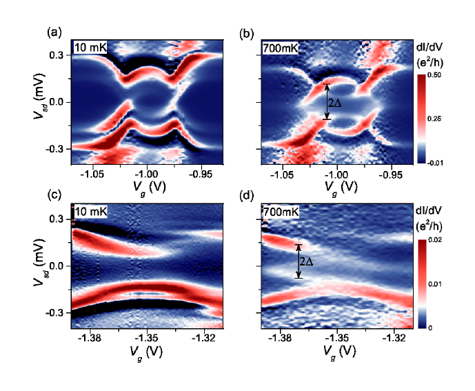
Having characterized the gate-tunable 0- transition of the Josephson junction in a InSb NWQD device, we now focus on the thermal effect on the two types of ABSs. Figs. 2(a) and 2(c) show the differential conductance in two types of Kondo valleys as a function of bias voltage and backgate voltage measured at base temperature and zero magnetic field. As mentioned above, depending on the respective ratio of , the main ABSs resonances behave as a crossing in Fig. 2(a), indicating the charge state is in a state in the middle of this region, while in Fig. 2(c) the noncrossing ABSs resonances denote a 0 state of that region. When the temperature is elevated gradually up to 700 mK, several prominent features of the ABSs resonances emerge in both state and 0 state regions. First we look at the state case (Fig. 2(b)). As the temperature is increased to 700 mK, the inner weak replicas – stem from the the alignment of residual density of states of quasiparticles in the probe at the Fermi level with the ABS levels - almost disappear. This could be explained by the thermal smearing of the quasiparticle DOS at the Fermi level. Moreover, the -type ABSs in the center of the Coulomb valley extend out of the state region while the 0-type ABSs outside of the crossing points penetrate into the state region, these extending structures form continuous resonances which are parallel to the original ABSs resonances at opposite at base temperature. For the 0 state case in Figs. 2(c) and 2(d), beside the main ABSs peaks, there are no inner structures at the base temperature. However, a new pair of weak resonances develop as the temperature is increased to 700 mK and similarly to the state case in Fig. 2(b), the newly developed resonances are parallel to the original ABSs resonances at opposite . A more detailed study of the ABSs spectroscopy at a series of elevated temperatures is given in section III of supplementary material. We note that both the main ABSs resonances and their replicas shift towards lower energies in the same way due to the shrink of as the temperature is increased, suggesting the same origin of these subgap features.
The evolution of the observed ABSs spectroscopy on temperature can be understood in term of thermally excited quasiparticle transport in the subgap regionKumar . As the temperature is elevated, quasiparticles can be thermally excited from the lower electron-like ABS to the upper hole-like ABS. As a consequence, charge transport through the thermally populated ABS level could be expected to generate additional resonant peaks in differential conductance at finite bias when the singularity of the BCS density of states of the probe is aligned with the thermally populated ABS. Hence these resonances are supposed to occur at . Given the condition for the original ABS resonances to occur, i.e. , the position of the thermally developed resonance and that of the original ABS resonance at finite bias corresponding to the same ABS level are spontaneously parallel with a constant spacing of 2. Therefore, these thermally-induced subgap features in the Andreev spectrum can also be viewed as replicas of the original ABS resonances. We also note that the width of the newly developed resonances exhibits a clear level broadening with increasing temperature, being consistent with the thermally populated ABS model. Compared with previous study, e.g. ref [37], we have observed the thermally developed ABS resonances in both -type ABS region and 0-type ABS region, thus constituting a complete experimental picture of the thermal population of different types of ABSs.
IV. ANDREEV BOUND STATES IN THE S-NWQD-S DEVICE
A. Coexistence of 0 and -type ABSs in the S-NWQD-S device.
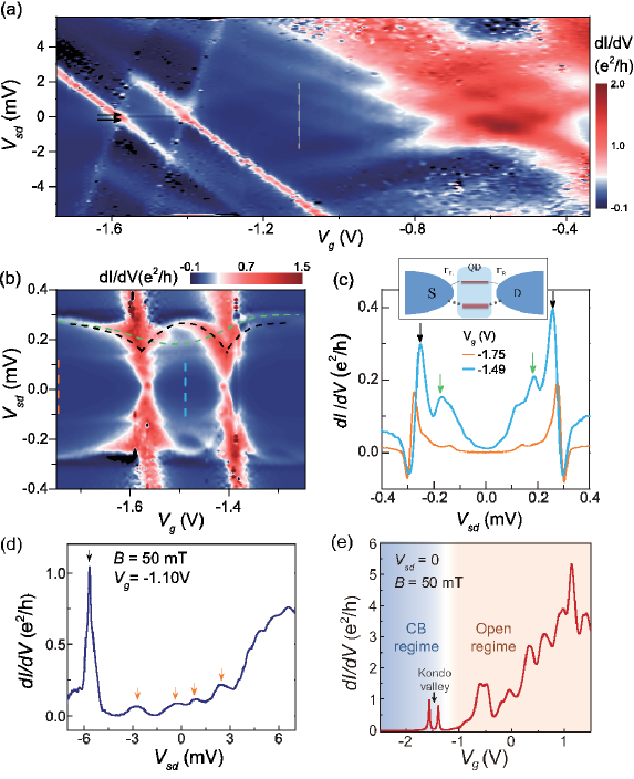
We now consider another case of a S-NWQD-S device and focus on the formation (and the underlying physical mechanism) of the ABSs with unusual appearances. We first characterize the device with the leads in the normal state. Fig. 3(a) presents differential conductance as a function of and measured at the base temperature with a small magnetic field applied ( mT). For the right region at -1.2 V, the transport is in a relatively open regime, where the average differential conductance is high and exhibits a series of broad resonances at low bias voltages. As the gate voltage becomes more negative, the differential conductance becomes lower with the emergence of a characteristic Coulomb diamond in the 2D plot, denoting the formation of a well defined QD. The charging energy can be estimated from the size of diamond as meV. Looking more closely at the diamond region, two narrow ridges of high conductance around zero bias, indicated by the black arrows, can be clearly seen in the Coulomb valley (see Fig. S4(b) in supplementary material), suggesting the emergence of a Kondo resonance. By measuring the temperature dependence and magnetic field evolution of the in the middle of the odd region (see Fig. S4(c) in supplementary material), we further verify that this split structure is a Kondo feature split by the Zeeman energy resulting from the large g-factor in InSb. From the magnetic field dependence of the Kondo splitting, we extract an effective g-factor of this Kondo valley: (see Fig. S4(d) in supplementary material). From the Lorentzian fit of the zero-bias conductance in the middle of the Kondo valley as a function of the magnetic field, the zero-bias conductance of Kondo ridge at is estimated to be , and the asymmetry ratio is obtained from the relation Gmax This high asymmetry ratio indicates that our device can be viewed as a tunneling probe model in which the ABSs are generated mainly between the QD and the strongly coupled lead, and are probed by the other weakly coupled leadDeacon ; Kim ; Tarucha07 ; Eichler07 .
Next we turn to look at the superconducting state spectrum of the device. Differential conductance as a function of and of the Kondo region measured at and the base temperature is displayed in Fig. 3(b). While the transport at the gate region away from the left resonant point ( V) is dominated by multiple Andreev reflections, with a quasiparticle cotunneling peak at and a weak first-order multiple Andreev reflection peak at , the Kondo valley exhibits rich subgap structures. Beside the weak first-order multiple Andreev reflection at , we concentrate on the main ABS resonance peaks which vary in the finite bias range from to as a function of the gate voltage. The most noticeable feature is that there are two different types of ABSs peaks of opposite curvature in dispersion of coexisting in this Kondo valley region, namely the -type crossed ABSs at outer positions(green dashed lines) and the 0-type noncrossed ABSs at inner positions (black dashed lines). This is more clearly characterized by two pairs of subgap peaks in Fig. 3(c), showing the line cut of in the middle of the Kondo valley in Fig. 3(b). In addition, these ABSs resonances appear to extend into the open regime region next to the Kondo valley, forming a set of weak ABSs resonances in the open region. As we have mentioned, the dispersion of two types of ABSs in the Kondo states is dominated by the system’s ground state - singlet or doublet - depending on the ratio . Taking total coupling strength as determined from the Coulomb resonance peaks of N state, the Kondo temperature at the middle of this valley can be estimated from the Bethe-Ansatz modelEichler09 ; Bethe as: mK (see section IV of supplementary material), which is much smaller than . From the magnetic field evolution of , a splitting of the Kondo resonance is observed already at a minimum field mT, corresponding to a Zeeman energy of eV, providing further evidence of the small value of . Therefore, this odd charge state is expected in a state, and one would expect only a pair of -type ABSs, being inconsistent with experimental observation. To understand the observed coexistence of the two types to ABSs, we propose a simple model, in which the transport processes in our device involve two parallel conduction channels with different coupling strength to the superconducting leads, which is illustrated in the inset of Fig. 3(c). Here, one channel is weakly coupled to the electrodes and sustains the weak Kondo correlation, leading to the formation of -type ABS. The other channel, which is strongly coupled to the electrodes, accounts for the emergence of the 0-type ABS. We now discuss the detailed mechanism about the two channel model in the following paragraph.
In fact, looking more closely at the normal state conductance plot in Fig. 3(a), we can see some broad resonances with crossed diagonal shapes at low bias on the right side of the Kondo charge state. For better clarity, we take a line cut in this region (grey dashed line) and plot the curve in Fig. 3(d). A set of quasi-periodic broad resonances at low bias could be clearly recognized. We argue that these broad resonances is the manifestation of the Fabry-Pérot interference in a ballistic nanowire. Fabry-Pérot interference patterns have been observed in InSb nanowire Josephson junctions in our previous workSenInSbJJ and a mean free path nm of our InSb nanowires has been extracted. Given here the channel length nm, the NWQD device is supposed to work in the ballistic regime and the occurrence of the Fabry-Pérot interference in the open regime is quite reasonable. Moreover, we can extract the average energy spacing of the Fabry-Pérot resonances from Fig. 3(d) as meV. Using the expression of energy spacing of the Fabry-Pérot interference in a 1D subband , where is the electron effective mass and is the cavity length, we calculate an effective cavity length nm, which is quite consistent with the geometric channel length of the device and thus supports our interpretation. Therefore, beside the weakly coupled quantum dot level, an additional channel with stronger coupling constituted by the Fabry-Pérot resonant states could also contribute to transport. Since the device shows a quick transition from the Coulomb blockade regime to open transport regime and the Kondo valley is just next to the transitional region (Fig. 3(e)), it is very likely that these two channels with different coupling strengths are involved in the transport simultaneously, which is also supported by the curve in Fig. 3(d) where the Fabry-Pérot resonances at low bias and the sharp tunneling resonance at high bias are observed simultaneously. Hence, the coexistent 0-type and -type ABS could be reasonably understood on the basis of such a two-channel model.
B. Temperature evolution of the coexistent 0 and -type ABSs.
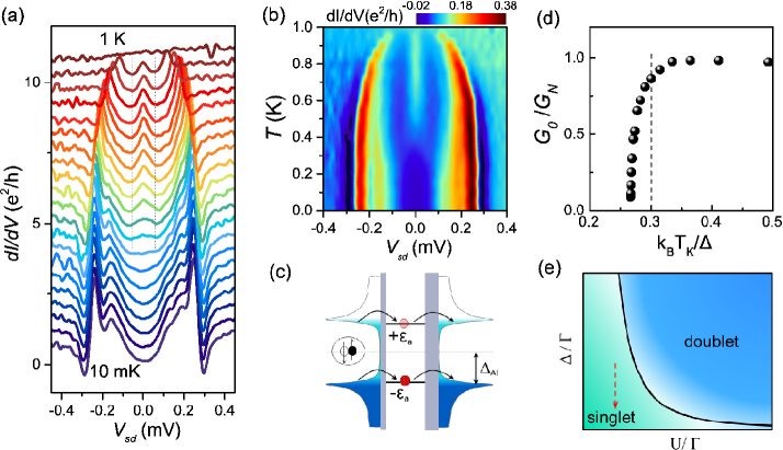
To better understand the properties of the coexistent 0 and -type ABSs, we measure the differential conductance along the cut in the middle of the Kondo valley (blue dashed line in Fig. 3(b)) over a wide range of temperature. The colored curves shown in Fig. 4(a) correspond to different temperatures, ranging from base temperature (10 mK) to the critical temperature of the Al leads ( 1 K), and they are plotted as a 2D graph in Fig. 4(b) (a temperature evolution of the overall spectra is given in Fig. S5 in supplementary material). From Figs. 4(a) and 4(b), we can see that the differential conductance barely changes in a low temperature range, i.e. mK. However, as the temperature is further elevated, several features become pronounced. First, the most prominent feature is the emergence of a zero bias conductance peak (ZBCP), rising up from approximately 400 mK. An ABS-assisted resonant tunneling process can lead to such ZBCP, as depicted in Fig. 4(c). Specifically, quasiparticles in the superconducting leads could be thermally excited from the continuum band below the Fermi level to the empty band above as temperature increases, occupying the density of state near the upper gap edge. Meanwhile the same process occurs between a pair of ABSs, leaving each level of the ABSs partially occupied. Note that inside the Kondo region the position of the -type ABSs is very close to the superconducting gap edge. Thus the thermally excited quasiparticles in the superconducting contacts could tunnel through the quantum dot via both -type ABSs near the two edges of the gap.
Although the scenario presented above is most likely to account for our observation, we also note that some features of the temperature dependence of the differential conductance in Fig. 4(a) can’t be fully explained by a thermally activated process. First, we find the width of the ZBCP changes little with increasing temperature, as indicated by the dotted line in Fig. 4(a). If the observed ZBCP is due to thermally excited quasiparticle transport, then the width of conductance peak should be broadened with increasing temperature, inconsistent with experimental result. Second, the temperature dependence of the ZBCP does not follow an exponential behavior as expected for a thermally activated process. In Fig. 4(d) we plot as a function of , where is the zero bias conductance and is the normal state conductance at high bias of each curve in Fig. 4(a). The ratio of first rises rapidly at small , then tends to saturate as becomes larger corresponding to the increase of temperature. The transition of these two trends occurs at roughly , which is coincident with theoretical predictions for the 0- transition to occurBauer ; Belzig . In a weak coupling regime, , the system is in the -state. As the temperature is raised, is reduced changing the relative strength of and , undergoing a crossover from state to 0 state. In the 0 state, Kondo resonance develops even in the presence of the superconducting gap, and contributes an conductance peak in equilibrium regime. Therefore, we speculate that it is likely that a temperature induced 0- transition is also responsible for the emergence of the observed ZBCP. Another interesting appearance, shown in Fig. 4(b), is that the 0-type ABSs at finite bias slightly shift to higher energy as the temperature increases above 300 mK. To understand this behavior, we look at the schematic phase diagram in the parameter space shown in Fig. 4(e), where represents the superconducting gap, the coupling strength between QD level and superconducting leads, and the charging energy, respectivelyBauer ; Squid . When temperature is increased in the range of K, is suppressed while no noticeable change of is expected, resulting in a reduced ratio of , represented by the red dashed line in the phase diagram in Fig. 4(e). Theoretically the ABSs tend to approach the continuum of the BCS band in the strong coupling limit Bauer ; Simon , hence the shift of 0-type ABSs towards higher energy (gap edge) with increasing temperature can be reasonably understood.
C. Magnetic field evolution of the coexistent 0 and -type ABSs.
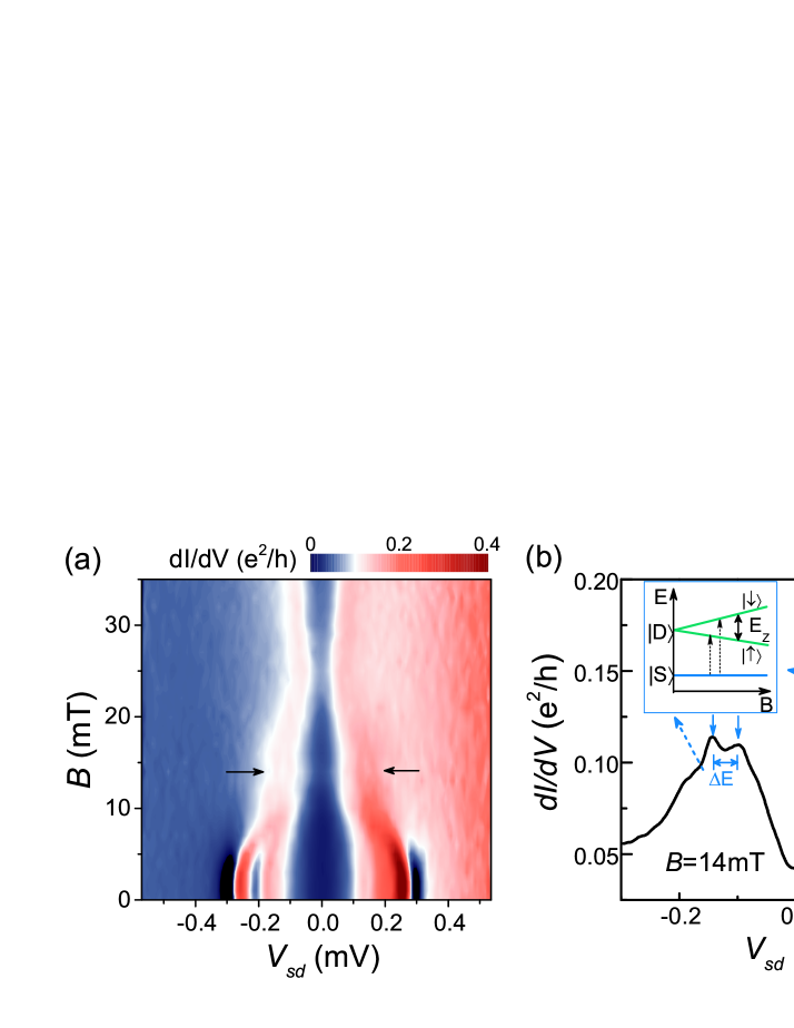
Finally, we explore the effect of magnetic field on the spectroscopy of ABSs. Fig. 5(a) displays the magnetic field evolution of the differential conductance measured along the blue dashed line cut in Fig. 3(b). As the magnetic field is applied, the energy of both -type ABSs and 0-type ABSs tends to decrease. Surprisingly the -type ABSs seem to decrease in an unusual fast way and become hardly distinguishable at mT – far below the superconductor critical field mT. The 0-type ABSs, on the other hand, vary much more slowly compared with the -type ABSs and remain to be resolved as the magnetic field approaches . Above the critical field, the ABSs peaks are replaced by a split Kondo resonance. In the presence of a magnetic field, two mechanisms that may have impact on the ABSs should be considered. On the one hand, the superconducting gap is suppressed by increasing magnetic field, which should result in a subsequent suppression of the intragap states and may also change the relative strength between Kondo correlation and superconductivity, making it possible for a 0- transition to happensilvanoPRL . But this effect is not supposed to be obvious until the magnetic field approaches since changes little at magnetic fields far below . On the other hand, the Zeeman effect will alter the energy of different types of ABSs, depending on the magnetic property of corresponding ground state, i.e. singlet or doublet. For a relatively small magnetic field, few tens of mT in our case, one might think of negligible effect of the Zeeman energy. However, considering the large g factors in InSb nanowires, the role of the Zeeman effect can not be neglected.
The energy of the -type ABSs is expected to increase in a magnetic field as a result of the Zeeman splitting of its doublet GSsilvanoNN (see lower right inset of Fig. 5(b)). But in our case, the -type ABS is quite close to the superconducting gap edge. Taking the level-repulsion effectsilvanoNN between the ABSs and the continuum of quasiparticle states into account, it is reasonable that we could not observe an increase of the energy of -type ABSs. As already mentioned, the -type ABSs are related with the QD level that is weakly coupled to the superconducting contacts. Such weakly coupled level may be localized in the NW segment just in the middle of the junction by the thick barriers, while the strongly coupled level related with the 0-type ABSs could extend in a longer geometric range. Hence, we attribute the rapid shrink of the -type ABS to the existence of magnetic flux focusing from the Meissner effect in the case of a narrow Josephson junction geometryGiazotto . As for the 0-type ABSs, in a finite magnetic field, they will also follow the suppression of . Besides, a splitting in such ABSs is also expected due to the Zeeman splitting of doublet ES (upper left inset of Fig. 5(b)). In our data, the 0-type ABSs show an overall decreasing trend as increases. Considering the relatively low magnetic field we apply limited by the critical field of Al, in such magnetic field range, the shrink of the gap is much more significant than the Zeeman energy. Thus the level repulsion effect between the ABS and the continuum of quasiparticle states leads to the overall decreasing trend of the 0-type ABSs. Nevertheless, we note that there is a sign of Zeeman splitting in the 0-type ABSs at mT indicated by the black arrows in Fig. 5(a). The corresponding is shown in Fig. 5(b), in which we are able to identify a split double-peak on both 0-type ABSs peaks. The energy distance between the double peaks is measured as eV. Using estimated from the Zeeman splitting of the Kondo resonance, we obtain a Zeeman energy eV at mT, which is consistent with the spacing of the double peaks, further supporting our interpretation.
V. CONCLUSION
In summary, we demonstrate gate tunable ABSs of different types in superconductor coupled InSb nanowire QDs with different device structures by transport measurements. The thermal effect on the two types of ABSs is extensively explored in the NWQD-SQUID devices and is understood with a thermally excited quasiparticle model. Two types of ABSs are observed simultaneously in the same charge state in a S-QD-S device, and explained in the senario of two conducting levels with different coupling strength to the leads. The evolution in elevated temperatures and magnetic field confirms the different natures of these ABSs. Therefore, despite the different device geometries, the spectroscopy of two types of ABSs in superconductor coupled single InSb QDs has been unambiguously displayed. Together with the variation of these ABSs, the 0- transition process driven by different physical parameters - gate voltage (in SQUID device) or temperature (in S-NWQD-S device) - has been revealed in such hybrid systems. Moreover, our work is the first systematic study of the tunable subgap bound states and 0- transition in InSb nanowire based hybrid superconducting systems which is an important candidate to host Majorana bound states. These results demonstrate the key role of Andreev Bound States in the transport in mesoscopic Josephson junctions and indicate potential prospect in exploring intragap bound states such as Majorana bound states in such systems.
ACKNOWLEDGMENTS
We thank D. X. Fan, G. Y. Huang and L. Lu for helpful discussions. This work was financially supported by the National Basic Research Program of the Ministry of Science and Technology of China (Nos. 2012CB932703 and 2012CB932700), and by the National Natural Science Foundation of China (Nos. 11374019, 91221202, 91421303, and 61321001). H. Q. Xu acknowledges also financial support from the Swedish Research Council (VR).
References
References
- (1) S. De Franceschi, L. Kouwenhoven, C. Schönenberger and W. Wernsdorfer, Hybrid Superconductor-Quantum Dot Devices, Nature Nanotech. 5, 703 (2010).
- (2) Y. J. Doh, J. A. van Dam, A. L. Roest, E. P. Bakkers, L. P. Kouwenhoven and S. De Franceschi, Tunable Supercurrent through Semiconductor Nanowires, Science 309, 272 (2005).
- (3) P. Jarillo-Herrero, J. A. van Dam and L. P. Kouwenhoven, Quantum Supercurrent Transistors in Carbon Nanotubes, Nature (London) 439, 953 (2006).
- (4) J. Xiang, A. Vidan, M. Tinkham, R. M. Westervelt and C. M. Lieber, Ge/Si Nanowire Mesoscopic Josephson Junctions, Nature Nanotech. 1, 208 (2006).
- (5) J. P. Cleuziou, W. Wernsdorfer, V. Bouchiat, T. Ondarcuhu and M. Monthioux, Carbon Nanotube Superconducting Quantum Interference Device, Nature Nanotech. 1, 53 (2006).
- (6) H. A. Nilsson, P. Samuelsson, P. Caroff and H. Q. Xu, Supercurrent and Multiple Andreev Reflections in an InSb Nanowire Josephson Junction, Nano Lett. 12, 228 (2012).
- (7) L. Hofstetter, S. Csonka, J. Nygård and C. Schönenberger, Cooper Pair Splitter Realized in a Two-Quantum-Dot Y-Junction, Nature (London) 461, 960 (2009).
- (8) L. G. Herrmann, F. Portier, P. Roche, A. L. Yeyati, T. Kontos and C. Strunk, Carbon Nanotubes as Cooper-Pair Beam Splitters, Phys. Rev. Lett. 104, 026801 (2010).
- (9) A. Das, Y. Ronen, M. Heiblum, D. Mahalu, A. V. Kretinin and H. Shtrikman, High-Efficiency Cooper Pair Splitting Demonstrated by Two-Particle Conductance Resonance and Positive Noise Cross-Correlation, Nature Commun. 3, 1165 (2012).
- (10) R. S. Deacon, A. Oiwa, J. Sailer, S. Baba, Y. Kanai, K. Shibata, K. Hirakawa and S. Tarucha, Cooper Pair Splitting in Parallel Quantum Dot Josephson Junctions, Nature Commun. 6, 7446 (2015).
- (11) J. Bauer, A. Oguri and A. C. Hewson, Spectral Properties of Locally Correlated Electrons in a Bardeen-Cooper-Schrieffer Superconductor, J. Phys.: Condens. Matter 19, 486211 (2007).
- (12) R. S. Deacon, Y. Tanaka, A. Oiwa, R. Sakano, K. Yoshida, K. Shibata, K. Hirakawa and S. Tarucha, Tunneling Spectroscopy of Andreev Energy Levels in a Quantum Dot Coupled to a Superconductor, Phys. Rev. Lett. 104, 076805 (2010).
- (13) J. D. Pillet, C. H. L. Quay, P. Morfin, C. Bena, A. L. Yeyati and P. Joyez, Andreev Bound States in Supercurrent-Carrying Carbon Nanotubes Revealed, Nature Phys. 6, 965 (2010).
- (14) J. D. Pillet, P. Joyez, R. Žitko and M. F. Goffman, Tunneling Spectroscopy of a Single Quantum Dot Coupled to a Superconductor: From Kondo Ridge to Andreev Bound States, Phys. Rev. B 88, 045101 (2013).
- (15) T. Meng, S. Florens and P. Simon, Self-Consistent Description of Andreev Bound States in Josephson Quantum Dot Devices, Phys. Rev. B 79, 224521 (2009).
- (16) J. Baranski and T. Domanski, In-Gap States of a Quantum Dot Coupled between a Normal and a Superconducting Lead, J. Phys.: Condens. Matter 25, 435305 (2013).
- (17) A. V. Rozhkov and D. P. Arovas, Josephson Coupling through a Magnetic Impurity, Phys. Rev. Lett. 82, 2788-2791 (1999).
- (18) E. Vecino, A. Martín-Rodero and A. Yeyati, Josephson Current through a Correlated Quantum Level: Andreev States and Junction Behavior, Phys. Rev. B 68, 035105 (2003).
- (19) F. Siano and R. Egger, Josephson Current through a Nanoscale Magnetic Quantum Dot, Phys. Rev. Lett. 93, 047002 (2004).
- (20) M.-S. Choi, M. Lee, K. Kang and W. Belzig, Kondo Effect and Josephson Current through a Quantum Dot between Two Superconductors, Phys. Rev. B 70, 020502 (2004).
- (21) J. S. Lim and M.-S. Choi, Andreev Bound States in the Kondo Quantum Dots Coupled to Superconducting Leads, J. Phys.: Condens. Matter 20, 415225 (2008).
- (22) M. R. Buitelaar, T. Nussbaumer and C. Schönenberger, Quantum Dot in the Kondo Regime Coupled to Superconductors, Phys. Rev. Lett. 89, 256801 (2002).
- (23) C. Buizert, A. Oiwa, K. Shibata, K. Hirakawa and S. Tarucha, Kondo Universal Scaling for a Quantum Dot Coupled to Superconducting Leads, Phys. Rev. Lett. 99, 136806 (2007).
- (24) A. Eichler, M. Weiss, S. Oberholzer, C. Schönenberger, A. Levy Yeyati, J. C. Cuevas and A. Martín-Rodero, Even-Odd Effect in Andreev Transport through a Carbon Nanotube Quantum Dot, Phys. Rev. Lett. 99, 126602 (2007).
- (25) T. Sand-Jespersen, J. Paaske, B. M. Andersen, K. Grove-Rasmussen, H. I. Jørgensen, M. Aagesen, C. B. Sørensen, P. E. Lindelof, K. Flensberg and J. Nygård, Kondo-Enhanced Andreev Tunneling in InAs Nanowire Quantum Dots, Phys. Rev. Lett. 99, 126603 (2007).
- (26) E. J. H. Lee, X. Jiang, R. Aguado, G. Katsaros, C. M. Lieber and S. De Franceschi, Zero-Bias Anomaly in a Nanowire Quantum Dot Coupled to Superconductors, Phys. Rev. Lett. 109, 186802 (2012).
- (27) B.-K. Kim, Y.-H. Ahn, J.-J. Kim, M.-S. Choi, M.-H. Bae, K. Kang, J. S. Lim, R. López and N. Kim, Transport Measurement of Andreev Bound States in a Kondo-Correlated Quantum Dot, Phys. Rev. Lett. 110, 076803 (2013).
- (28) Y. Kanai, R. S. Deacon, A. Oiwa, K. Yoshida, K. Shibata, K. Hirakawa and S. Tarucha, Electrical Control of Kondo Effect and Superconducting Transport in a Side-Gated Inas Quantum Dot Josephson Junction, Phys. Rev. B 82, 054512 (2010).
- (29) R. M. Lutchyn, J. D. Sau and S. Das Sarma, Majorana Fermions and a Topological Phase Transition in Semiconductor-Superconductor Heterostructures, Phys. Rev. Lett. 105, 077001 (2010).
- (30) Y. Oreg, G. Refael and F. von Oppen, Helical Liquids and Majorana Bound States in Quantum Wires, Phys. Rev. Lett. 105, 177002 (2010).
- (31) W. Chang, V. E. Manucharyan, T. S. Jespersen, J. Nygård and C. M. Marcus, Tunneling Spectroscopy of Quasiparticle Bound States in a Spinful Josephson Junction, Phys. Rev. Lett. 110, 217005 (2013).
- (32) E. J. Lee, X. Jiang, M. Houzet, R. Aguado, C. M. Lieber and S. De Franceschi, Spin-Resolved Andreev Levels and Parity Crossings in Hybrid Superconductor-Semiconductor Nanostructures, Nature Nanotech. 9, 79 (2014).
- (33) J. A. van Dam, Y. V. Nazarov, E. P. Bakkers, S. De Franceschi and L. P. Kouwenhoven, Supercurrent Reversal in Quantum Dots, Nature (London) 442, 667 (2006).
- (34) H. I. Jørgensen, T. Novotny, K. Grove-Rasmussen, K. Flensberg and P. E. Lindelof, Critical Current 0- Transition in Designed Josephson Quantum Dot Junctions, Nano Lett. 7, 2441 (2007).
- (35) A. Eichler, R. Deblock, M. Weiss, C. Karrasch, V. Meden, C. Schönenberger and H. Bouchiat, Tuning the Josephson Current in Carbon Nanotubes with the Kondo Effect, Phys. Rev. B 79, 161407 (2009).
- (36) R. Maurand, T. Meng, E. Bonet, S. Florens, L. Marty and W. Wernsdorfer, First-Order 0- Quantum Phase Transition in the Kondo Regime of a Superconducting Carbon-Nanotube Quantum Dot, Phys. Rev. X 2, 011009 (2012).
- (37) A. Kumar, M. Gaim, D. Steininger, A. L. Yeyati, A. Martín-Rodero, A. K. Hüttel and C. Strunk, Temperature Dependence of Andreev Spectra in a Superconducting Carbon Nanotube Quantum Dot, Phys. Rev. B 89, 075428 (2014).
- (38) T. Dirks, T. L. Hughes, S. Lal, B. Uchoa, Y.-F. Chen, C. Chialvo, P. M. Goldbart and N. Mason, Transport through Andreev Bound States in a Graphene Quantum Dot, Nature Phys. 7, 386 (2011).
- (39) H. A. Nilsson, P. Caroff, C. Thelander, M. Larsson, J. B. Wagner, L.-E. Wernersson, L. Samuelson and H. Q. Xu, Giant, Level-Dependent g Factors in Insb Nanowire Quantum Dots, Nano Lett. 9, 3151 (2009).
- (40) S. Nadj-Perge, V. S. Pribiag, J. W. van den Berg, K. Zuo, S. R. Plissard, E. P. Bakkers, S. M. Frolov and L. P. Kouwenhoven, Spectroscopy of Spin-Orbit Quantum Bits in Indium Antimonide Nanowires, Phys. Rev. Lett. 108, 166801 (2012).
- (41) D. Fan, S. Li, N. Kang, P. Caroff, L. B. Wang, Y. Q. Huang, M. T. Deng, C. L. Yu and H. Q. Xu, Formation of Long Single Quantum Dots in High Quality InSb Nanowires Grown by Molecular Beam Epitaxy, Nanoscale 7, 14822 (2015).
- (42) V. Mourik, K. Zuo, S. M. Frolov, S. R. Plissard, E. P. A. M. Bakkers and L. P. Kouwenhoven, Signatures of Majorana Fermions in Hybrid Superconductor-Semiconductor Nanowire Devices, Science 336, 1003 (2012).
- (43) M. T. Deng, C. L. Yu, G. Y. Huang, M. Larsson, P. Caroff and H. Q. Xu, Anomalous Zero-Bias Conductance Peak in a Nb-InSb Nanowire-Nb Hybrid Device, Nano Lett. 12, 6414 (2012).
- (44) M. T. Deng, C. L. Yu, G. Y. Huang, M. Larsson, P. Caroff and H. Q. Xu, Parity independence of the zero-bias conductance peak in a nanowire based topological superconductor-quantum dot hybrid device, Sci. Rep. 4, 7261-7268 (2014).
- (45) B. M. Andersen, K. Flensberg, V. Koerting and J. Paaske, Nonequilibrium Transport through a Spinful Quantum Dot with Superconducting Leads, Phys. Rev. Lett. 107, 256802 (2011).
- (46) K. Grove-Rasmussen, H. I. Jørgensen, B. M. Andersen, J. Paaske, T. S. Jespersen, J. Nygård, K. Flensberg and P. E. Lindelof, Superconductivity-Enhanced Bias Spectroscopy in Carbon Nanotube Quantum Dots, Phys. Rev. B 79, 134518 (2009).
- (47) S. Li, N. Kang, D. X. Fan, L. B. Wang, Y. Q. Huang, P. Caroff and H. Q. Xu, Coherent Charge Transport in Ballistic InSb Nanowire Josephson Junctions, Sci. Rep. 6, 24822 (2016).
- (48) K. Grove-Rasmussen, H. I. Jørgensen and P. E. Lindelof, Kondo Resonance Enhanced Supercurrent in Single Wall Carbon Nanotube Josephson Junctions, New J. Phys. 9, 124-124 (2007).
- (49) T. K. Ng and P. A. Lee, On-Site Coulomb Repulsion and Resonant Tunneling, Phys. Rev. Lett. 61, 1768-1771 (1988).
- (50) F. D. M. Haldane, Scaling Theory of the Asymmetric Anderson Model, Phys. Rev. Lett. 40, 416-419 (1978).
- (51) J. Paajaste, M. Amado, S. Roddaro, F. S. Bergeret, D. Ercolani, L. Sorba and F. Giazotto, Pb/InAs Nanowire Josephson Junction with High Critical Current and Magnetic Flux Focusing, Nano Lett. 15, 1803 (2015).
- (52) T. Xu, K. A. Dick, S. Plissard, T. H. Nguyen, Y. Makoudi, M. Berthe, J.-P. Nys, X. Wallart, B. Grandidier and P. Caroff, Faceting, Composition and Crystal Phase Evolution in III-V Antimonide Nanowire Heterostructures Revealed by Combining Microscopy Techniques, Nanotechnology 23, 095702 (2012).
- (53) C. Thelander, P. Caroff, S. b. Plissard and K. A. Dick, Electrical Properties of InAs1-xSbx and InSb Nanowires Grown by Molecular Beam Epitaxy, Appl. Phys. Lett. 100, 232105 (2012).