Synthetic photonic lattices: new routes towards all-optical photonic devices
Abstract
All-optical photonic devices are crucial for many important photonic technology and applications, ranging from optical communication to quantum information processing. Conventional design of all-optical devices is based on photon propagation and interference in real space, which may reply on large numbers of optical elements and are challenging for precise control. Here we propose a new route for engineering all-optical devices using photon internal degrees of freedom, which form photonic crystals in such synthetic dimensions for photon propagation and interference. We demonstrate this new design concept by showing how important optical devices such as quantum memory and optical filter can be realized using synthetic orbital angular momentum (OAM) lattices in a single main degenerate cavity. The new designing route utilizing synthetic photonic lattices may significantly reduce the requirement for numerous optical elements and their fine tuning in conventional design, paving the way for realistic all-optical photonic devices with novel functionalities.
I Introduction
The ability of coherently controlling the properties of photons, such as their storage and propagation, is crucial for many important technological applications in various fields, ranging from optical communications thevenaz2008slow ; vlasov2008high ; takesue2013chip , data storage yanik2004stopping2 ; baba2008slow ; lvovsky2009optical ; kuramochi2014large , to quantum information processing kimble2008quantum ; northup2014quantum . The devices used for such purpose may involve the interaction of photons with other physical media (e.g., atoms) lvovsky2009optical ; northup2014quantum or contain only optical elements, i.e., all-optical photonic devices yanik2004stopping2 ; baba2008slow ; vlasov2008high ; takesue2013chip ; kuramochi2014large . In conventional all-optical devices, photonic properties are controlled through manipulating the photon interference in the real space baba2008slow ; takesue2013chip . Typical examples include photonic crystals, where coupled arrays of photonic circuits are implemented by fine tuning the parameters of associated optical elements. The conventional all-optical photonic devices have been extensively studied and showcase great applications, ranging from practical devices baba2008slow ; vlasov2008high ; kuramochi2014large to fundamental topological photonics hafezi2011robust ; fang2012realizing ; lu2014topological . However, such real space photonic devices usually demand precise control of a large number () of spatially separated optical elements (e.g., resonators, waveguides, etc.) [see illustration in Fig. 1 (a)], which can be very complicated and resource-costing for many practical applications.
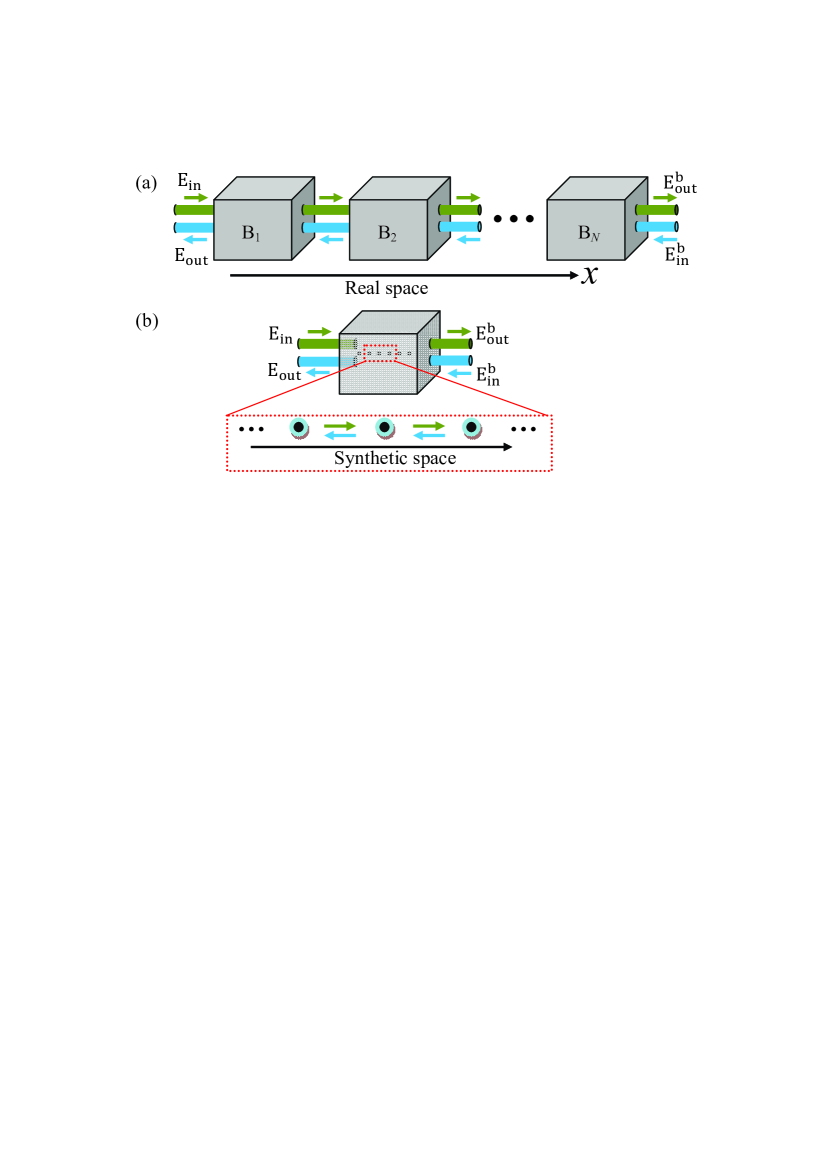
On the other hand, photons possess many internal degrees of freedom (e.g., frequency, polarization, orbital angular momentum (OAM) yariv2007photonics ; allen1992orbital , etc.), which may form synthetic lattice dimensions for photons (i.e., synthetic photonic crystals) in addition to real space. Recently synthetic lattice dimensions have been explored in ultra-cold atomic gases with the direct experimental observation of quantum Hall edge states PhysRevLett.112.043001 ; mancini2015observation ; stuhl2015visualizing . Here we propose a conceptually new route for engineering all-optical photonic devices based on photon propagation and interference in such synthetic photonic lattices [see Fig. 1 (b)], instead of a large number of optical elements in the real space photonic crystals. The all-optical devices based on such synthetic photonic lattices may significantly reduce the physical complexity of the system and are more resource-efficient.
In this article, we explore this new designing paradigm by showing how all-optical photonic devices can be implemented using photon propagation and interference in the synthetic lattices formed by photon OAM modes. Because of the large number of available distinctive OAM states, photon OAM has found great applications in quantum information fickler2014interface ; wang2015quantum ; malik2016multi , optical communications barreiro2008beating ; wang2012terabit , and the realization of topological matter luo2015quantum . Different discrete OAM states form a natural synthetic lattice for photon interference. We consider a degenerate-cavity system that supports multiple degenerate OAM modes, where the interference of photon in the OAM lattice can be manipulated by simply tuning an optical phase. We show that important photonic devices such as quantum memory and optical filter that are vital for quantum communication networking and optical signal processing can be realized using an OAM-based system with only a single main cavity, where the photon is stopped, stored, and read out on demand in the synthetic OAM lattice. The proposed all-optical quantum memory are more resource-efficient and experimentally simpler than conventional real-space coupled-cavity-based memory that requires precise control of a large number of coupled cavities yanik2004stopping . They have a large bandwidth and no restriction on the working frequency compared to atomic-ensemble-based memory simon2010quantum . The proposed route will not only motivate other novel applications and devices based on the OAM lattices, but also open a completely new avenue for engineering all-optical photonic devices utilizing other internal degrees of freedom (e.g., frequency, etc.) as synthetic lattice dimensions ozawa2016synthetic ; yuan2016photonic ; ozawa2016synthetic2 .
II Results
II.1 Photon OAM and coupled-degenerate-cavities
Solutions of the light field in an optical system with cylindrical symmetry have an angular dependence , where is the azimuthal angle and is an integer yariv2007photonics . This is a fundamental optical degree of freedom associated with the OAM of photons that has a value of per photon allen1992orbital . In comparison with other optical degrees of freedom, OAM has a fascinating property that an infinite number of distinctive OAM states are available. These discrete OAM states can be used to denote discrete lattice sites in the OAM-enabled synthetic lattice dimension.
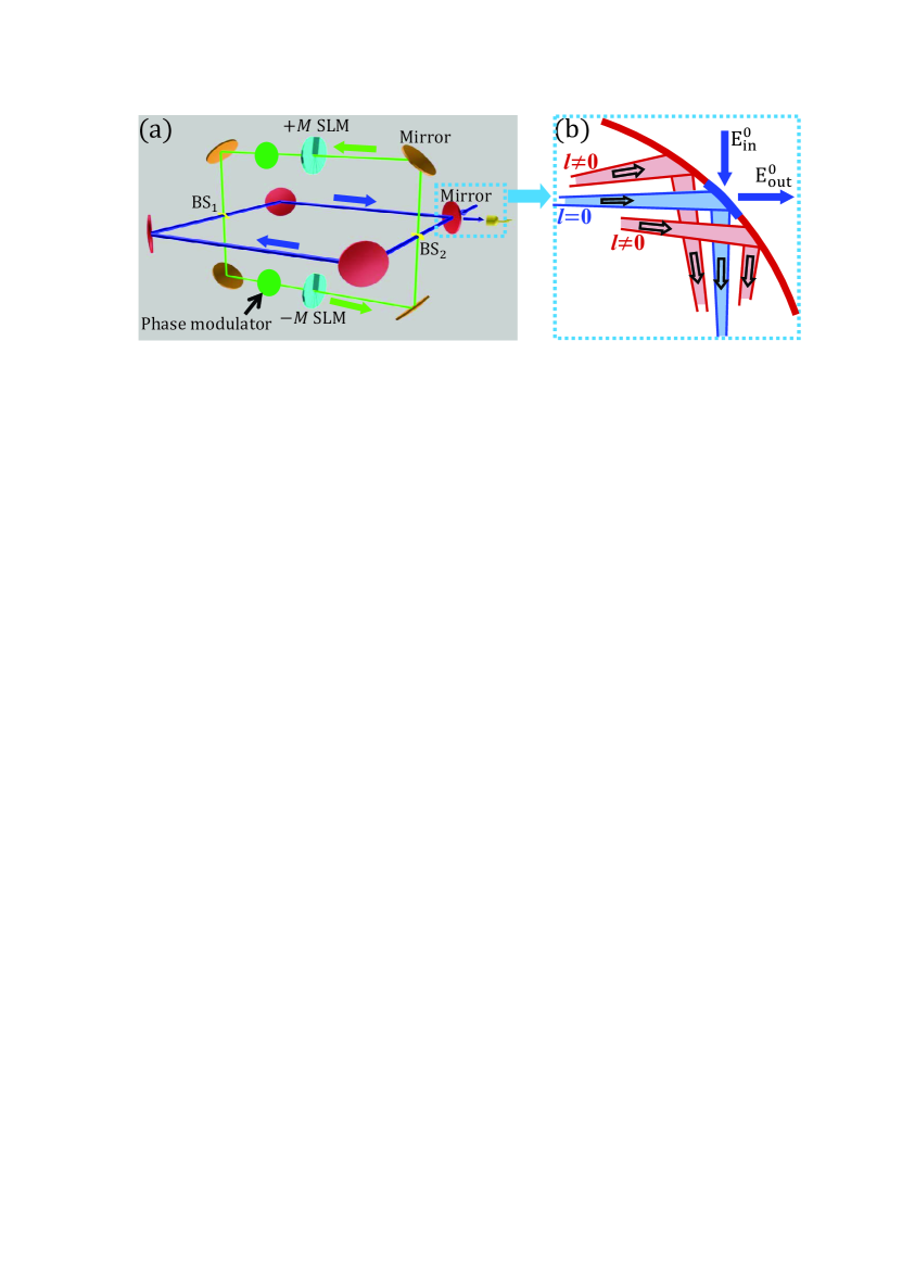
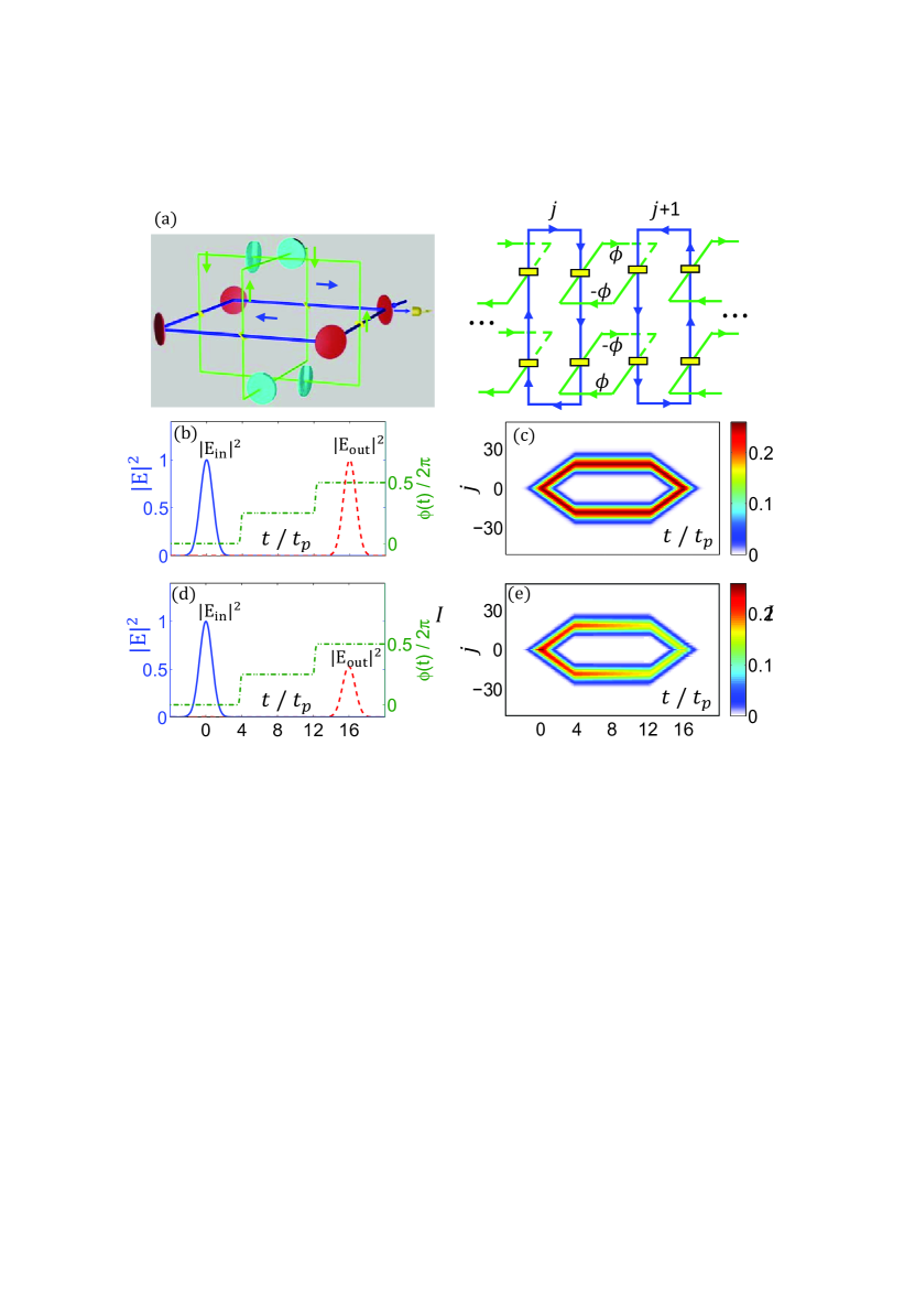
The OAM-based synthetic photonic lattices can be generated and manipulated using a degenerate cavity arnaud1969degenerate ; chalopin2010frequency that can support multiple OAM modes simultaneously. In experiments, such a degenerate cavity with a large number of OAM modes is easy to realize with a flexible configuration arnaud1969degenerate . The proposed all-optical photonic devices rely on the coupling between different OAM modes in the degenerate cavity for photon interference and propagation, which can be realized using an auxiliary cavity. The optical design, shown in Fig. 2(a), consists of a main degenerate cavity and an auxiliary degenerate cavity coupled by two beam splitters with low reflectivity. Unlike the main cavity, the length of the auxiliary cavity is chosen for destructive interference, therefore most photons remain in the main cavity. Two spatial light modulators (SLMs) such as very low-loss vortex phase plates oemrawsingh2005experimental are inserted into the auxiliary cavity, which couple OAM mode of the passing photons to its adjacent modes with with being the step index of the SLM. Two phase modulators placed in the two arms of the auxiliary cavity generate different phases for the coupling along two arms, which can be realized using, for instance, high-speed electro-optic index modulation chuang1995physics ; yariv2007photonics .
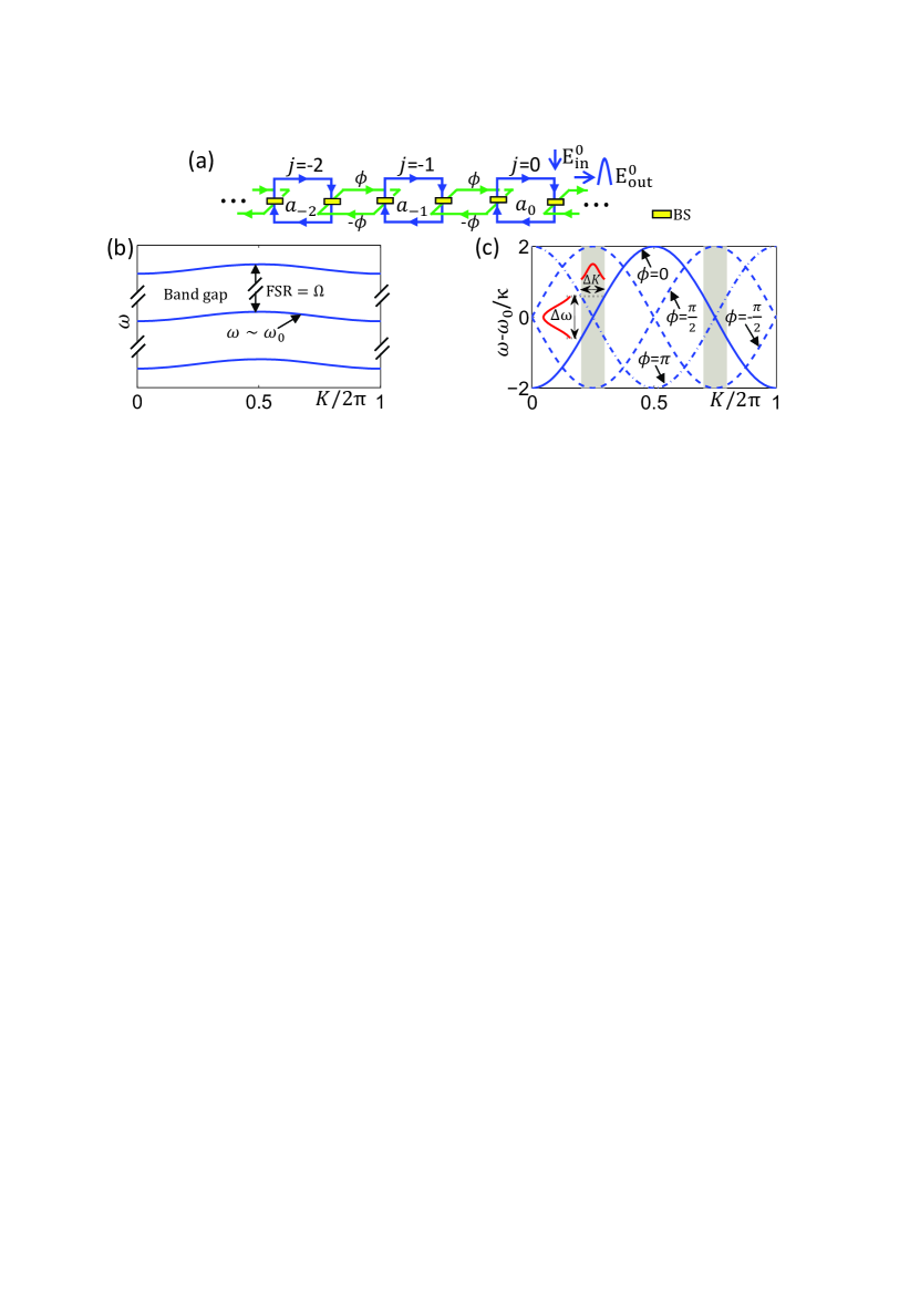
Interestingly, the single main cavity system in Fig. 2 is conceptually equivalent to a 1D array of coupled optical resonators luo2015quantum , which makes our scheme much simpler than previous coupled cavity based quantum devices that contain more than 100 cavity units each consisting of several carefully coupled and tuned cavities yanik2004stopping . This mapping is illustrated in Fig. 3 (a), where the -th state with an OAM number is associated with the position index of a cavity. In the weak coupling limit between auxiliary and main cavities, the Hamiltonian for the system in Fig. 3 (a) can be written as hafezi2011robust
| (1) |
in the OAM space, where is the annihilation operator of the cavity photon of OAM mode , is the phase imbalance between the two arms of the auxiliary cavity, and is the resonant frequency of the main cavity. The tunneling rate between OAM modes , where , and are the reflectivity and transmissivity of the coupling beam splitters, is the free spectral range (FSR) of the cavity, is the total length of the cavity optical path, and is the speed of light.
For the critical input and output channels of the photonic device, we introduce a low-reflectivity pinhole at the center of the input/output mirror as shown in Fig. 2 (b), which can be implemented using, for instance, graded coating piegari1996coatings . This is a widely used technique barreiro2008beating ; wang2012terabit to differentiate mode from others since is the only mode with a high intensity at the beam center yariv2007photonics ; yao2011orbital . The rotationally symmetric pinhole does not affect the OAM number of the cavity modes, and it introduces a large loss rate for the and low OAM modes, since they can leak out of the cavity via the pinhole and couple to outside modes. In contrast, higher OAM modes, whose field distribution has negligible overlap with the pinhole, are hardly disturbed, just like a mode is not affected by the finite aperture of the mirror in a cavity (without a pinhole) though its wave front is infinite in theory (see Supplementary Materials). With proper choice of the step index , only mode in the cavity couples to the input/output field and has a significant rate of loss.
When photons propagate in all-optical devices, the time evolution of optical modes (in Heisenberg picture) is described by walls2008quantum
| (2) | |||||
where is the time-dependent field operator of OAM mode , is its loss rate, and is the input field operator which couples to the mode in the cavity at a rate determined by the reflectivity of the input/output pinhole. The input field operator is given by , with and being the annihilation operator of the input photon with frequency . The proposed devices work for both quantum single-photon and classical coherent state input pulses (see Supplementary Materials), since the dynamics of our system is characterized by the linear equation of photon operators (see Eq. 2).
The dispersion spectrum of the Hamiltonian (1) is
| (3) |
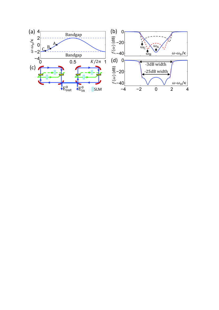
where is the system’s eigenfrequency, and is the Bloch wave number. Clearly the dispersion relation [see Figs. 3 (b) and 3 (c)] and the propagating group velocity in the OAM space can be manipulated by simply tuning the phase imbalance in experiments. Such tunability make it possible to realize important optical devices such as quantum memory and optical filter.
II.2 Quantum memory in synthetic OAM lattices
Quantum memory is a key element in many quantum information protocols kimble2008quantum ; lvovsky2009optical . Since information is encoded in photons in a quantum communication network, any non-optical element, such as atomic ensemble simon2010quantum , requires transferring of information from and back to photons, which complicates the operation of the quantum memory and lowers its efficiency. Furthermore, only a very limited number of elements are suitable for atomic-ensemble-based quantum memory, and the frequency range is restricted to available atomic transitions simon2010quantum . An all-optical quantum memory eliminates the need to transfer information between different physical media and can in principle lead to simplified operation and improved efficiency. However, existing schemes for all-optical quantum memory based on coupled optical resonators yanik2004stopping ; yanik2004stopping2 or modulation of index of refraction baba2008slow ; baba2008large have their own difficulties for fabricating large numbers of identical optical cavities or homogeneously tuning the index of optical materials.
An all-optical quantum memory based on slowing/stopping light through photon interference in the OAM lattice can overcome those difficulties of existing schemes and offer compelling advantages. The photon propagation is now slowed down in the OAM-enabled synthetic lattices by tuning the phase , which is much simpler and more reliable compared to simultaneous and precise tuning of hundreds of cavities for quantum memory based on coupled resonators in real dimension yanik2004stopping . The major operation procedure for the quantum memory consists of three steps by controlling the phase imbalance : i) writing the input signal into the memory by coupling to the mode in the cavity through the input pinhole; ii) letting the signal in the cavity propagate to certain high modes and storing it there for a desired storage time; iii) making the signal propagate back to the mode for read-out by coupling to the output through the same pinhole for write-in.
For a proof-of-principle illustration of our OAM-based quantum memory, we first ignore the loss of all modes and assume . As shown in Figs. 4 (a) and (b), if we design the system such that , the incoming signal pulse is absorbed into the cavity with an efficiency of 100% (see Supplementary Materials). In order to store pulses significantly shorter than the write-in time , the usable memory bandwidth poon2004designing should satisfy the condition simon2007quantum . Once in the cavity, all frequency components of the signal pulse start to propagate to modes. For a long storage time, the signal may propagate to high OAM numbers. Though there is no theoretical upper limit for the OAM number, in reality it is limited by practical factors such as the aperture size of the optical elements in the cavity.
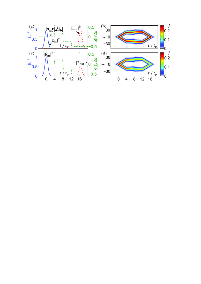
In order to limit the OAM number, we slow down the propagation of the signal pulse in the OAM space by tuning the phase imbalance . As illustrated in Figs. 4 (a) and (b), is set to 0 in the write-in process. When the signal pulse enters the cavity completely after a write-in time , its peak travels (in the OAM space) approximately at a group velocity . We then change the phase to adiabatically compared with the bandgap of the system approximately given by the FSR [Fig. 3 (b)]. The modulation of preserves the system’s translational symmetry in the OAM lattice, and thus the Bloch wave vectors of the signal is conserved. At , becomes 0 [see Fig. 3 (c)], and the pulse stops propagating in the OAM lattice as shown in Fig. 4 (b).
Meanwhile, the pulse starts to expand in the OAM lattice due to the dispersion of the spectrum, which causes distortion in the temporal profile of the signal. To correct this distortion and restore the signal to its original shape for read-out, we tune to and keep its value at for the same amount of time for which was set to . Finally, we tune to . As shown in Figs. 4 (a) and (b), after another period of time equal to the write-in time , the above phase echo procedure not only returns all frequency components of the signal to the mode, but also corrects any distortion accumulated in the first half of the process. The pulse can be read out with an efficiency of 100% under the condition and the total storage time . To ensure full emission, it is required that , with the maximum OAM state that the cavity can support.
Although the storage time of our OAM-based quantum memory is controllable, it is preset. We can freeze the photon signal in the OAM lattice and enable its on-demand recall by slightly modifying our design from the device in Fig. 2. The corresponding circuits are shown in Fig. 5 (a), which use two auxiliary cavities with the same coupling strength and opposite phase imbalances . Because of the interference between the two auxiliary cavities, the dispersion relation of the system becomes
| (4) |
The group velocities of the pulse peaks at become . Once the input signal is absorbed into the cavity, we can stop the pulse’s propagation and dispersion in the OAM lattice completely by adiabatically changing from 0 to , which compresses the bandwidth to 0 because transitions between OAM modes via the two auxiliary cavities cancel each other. As shown in Fig. 5, the optical signal and its distribution in the OAM lattice can then be kept for an arbitrary and indefinite amount of time until it needs to be read-out by changing from to . This allows the on-demand recall of the photon signal and random access to the quantum information that it carries. The storage fidelity of a single-photon pulse, which is defined as the wave-packet overlap between input and output conditional on the re-emission of a photon simon2010quantum , is close to 1. Thus it is possible to realize perfect write-in, storage, and on-demand read-out of an optical signal using only a limited number of OAM states sufficient for the signal pulse to be absorbed into the cavity.
In reality, all OAM modes are lossy due to factors such as intrinsic loss of the optical elements and leakage of modes via the input-output pinhole. It is demonstrated that (see Supplementary Materials), our OAM-based quantum memory still functions as expected without wave-packet distortion in the presence of imperfections, though the efficiency is reduced, as shown in Figs. 4 (c), (d) and Figs. 5 (d) and (e).
For the estimation of experimental parameters, we assume that the cavity is realized using four curved mirrors each with a focal length on the order of centimeters, a typical value for discrete optical elements. Since the separation between the mirrors is , the total length is about tens of centimeters for the optical path, which gives a FSR () of GHz - GHz. By choosing a proper reflectivity for the beam splitters, we estimate that the total bandwidth is about MHz - MHz. Therefore, the quantum memory can store short pulses with a temporal duration of tens of nanoseconds. The bandwidth can be further improved by using a smaller focal length . The required modulation time for the phase imbalance is also on the order of tens of nanoseconds, consistent with the modulation speed of current electro-optic devices chuang1995physics ; yariv2007photonics . With a photon loss rate of the order of MHz, the storage time is about s (see Supplementary Materials). As a comparison, the storage time of ideally identical coupled-micro-resonator based memory is limited below s due to the large photon losses of the micro-resonators (about tens of MHz) yanik2004stopping .
II.3 OAM-enabled optical filter
We can build upon our ideas to envision further interesting and valuable applications. One such example is high skirt-slope optical filters which are crucial in many fields such as quantum information palittapongarnpim2012note ; neergaard2006generation ; macrae2012tomography , high-density wavelength-division-multiplexing networking, and optical signal processing ilchenko2006optical ; minasian2001photonics ; little2004very . For good selectivity, the filter function should ideally have a narrow bandwidth and a steep skirt slope at the edge of the stopband. It is then critical to improve the shape factor which is often evaluated by the ratio of the stopband width at -25dB and -3dB minasian2001photonics ; little2004very . Conventionally, this is usually achieved by coupling many carefully designed cavities to obtain a high-order filter little2004very . Because of inevitable errors in fabrication and tuning, the number of cavities that can be reliably coupled in practice is quite limited. Consequently, it is very challenging to realize high shape factors in an optical filter based on many coupled cavities.
It is possible to achieve an optical filter with very high shape factors using the band spectrum Eq. (3) generated by the photon interference in the OAM lattice in Fig. 6. The filter characteristics can be obtained by analyzing the wave propagation in the coupled many-cavity system in Fig. 3 (a) which is a conceptual equivalent to our OAM-based device. However, a much more intuitive understanding based on the system spectrum is possible which can greatly facilitate the design of the filter to obtain desired properties. In the device in Fig. 2, when an signal is fed to the input/output port, all frequency components in the bandgaps cannot enter the cavity and are reflected. The cavity absorbs in-band frequency components with an efficiency dependent on the coupling rate and the group velocity of the cavity mode in the OAM lattice. The maximum absorption occurs at the frequency determined by (see Supplementary Materials). If we choose the reflectivities of the coupling beam splitter and input/output pinhole appropriately such that is very close to the cavity’s band edge , the cavity changes from being totally reflective to being strongly absorptive to the incident light over a narrow frequency range . This results in a desired steep skirt slope as shown in Fig. 6 (b). Unfortunately, because of the frequency dependence of the group velocity, for such a choice of the absorption is poor at the center of the stopband, leading to an insufficient in-band rejection ratio which manifests as the hump at the bottom of the filter function in Fig. 6 (b).
In order to overcome this difficulty, we use the two-cavity design in Fig. 6 (c). While the maximum absorption frequency of the first cavity is still chosen to be close to the band edge, that of the second cavity is chosen closer to the center of the stopband to suppress the hump in Fig. 6 (b). Such a design results in a narrow and deep stopband with sharp edges, which is ideal for optical filters.
Since the input and output fields are both in the mode, the filter function for our filter is calculated by luo2015quantum
| (5) |
with
| (6) |
where is an OAM state, is a Bloch state in the OAM space with frequency . As plotted in Fig. 6 (d), a shape factor of 0.85 can be realized with just moderate SLM and cavity efficiencies (see Supplementary Materials), which is noticeably higher than current technologies that are limited by the number of high-Q cavities that can be reliably coupled in practice little2004very ; savchenkov2009narrowband ; rasras2009demonstration .
III Discussion
Imperfections such as photon losses will degrade the performance of the optical devices. Intrinsic loss due to the finite finesse of the cavity can be very low as long as high quality cavities are used nagorny2003collective . Photon losses can also be introduced by phase modulators due to absorption by their optical media and SLMs because of their limited resolution and fabrication error. Such losses can be made very low leidinger2015highly ; oemrawsingh2005experimental ; marrucci2011spin ; raut2011anti (see Supplementary Materials), and further reduced by the fact that the auxiliary cavity is designed using destructive interference with very few photons in it. The low reflectivity pinhole manifests as an photon loss that decreases rapidly with the OAM number (see Supplementary Materials). For the quantum memory, the storage time (for a fixed storage efficiency) decreases rapidly with the increase of photon losses. Photon losses due to the phase modulators and SLMs are the limiting factors for the storage time, since their effect is persisting, even during the storage phase when the signal is frozen at large OAM states. We find that for the optical filter, the shape factor and stop bandwidth are less sensitive to imperfections of these optical elements, as confirmed by our numerical simulation.
Even with the limitations posed by these practical considerations, the OAM-based quantum memory has a few attractive characteristics and note-worthy advantages that are not available in existing schemes. Not only is the system very simple with just a single main cavity and thus completely realizable with conventional optical technology, but also the operating wavelength can be chosen at will, a significant edge in situations where no atomic systems with the desired transition frequency are available. It is also not limited by the technical challenge to fabricate and tune a large number of identical optical cavities yanik2004stopping . The bandwidth of the quantum memory and its storage time are limited by the size of the cavity and loss of the SLMs and phase modulators, instead of the delay-bandwidth product of the system or other intrinsic factors. Finally, polarization independent optical elements can be used so that information encoded in both temporal wave-packet and polarization can be recovered with fidelity close to 1.
In conclusion, we propose a conceptually novel route for engineering all-optical photonic devices based photon propagation and interference in synthetic lattices. We demonstrate this new designing principle by showing that two powerful devices, quantum memory and optical filter, can be realized utilizing photon OAM-based synthetic lattices. The proposed route may inspire new and simple designs for many other photonic devices (e.g., multi-channel optical router, etc.), and open a completely new avenue for photonic technology and applications.
IV Acknowledgements
This work is funded by NNSFC (Grant Nos. 11574294, 61490711), NKRDP (Grant Nos.2016YFA0301700 and 2016YFA0302700) and the ”Strategic Priority Research Program(B)” of the CAS (Grant No.XDB01030200). CZ is supported by ARO (W911NF-12-1-0334) and NSF (PHY-1505496).
References
- (1) Thévenaz, L. Slow and fast light in optical fibres. Nature Photon. 2, 474–481 (2008).
- (2) Vlasov, Y., Green, W. and Xia, F. High-throughput silicon nanophotonic wavelength-insensitive switch for on-chip optical networks. Nature Photon. 2, 242–246 (2008).
- (3) Takesue, H., Matsuda, N., Kuramochi, E., Munro, W. J. and Notomi, M. An on-chip coupled resonator optical waveguide single-photon buffer. Nature Commun. 4, 2725 (2013).
- (4) Yanik, M. F., Suh, W., Wang, Z. and Fan, S. Stopping light in a waveguide with an all-optical analog of electromagnetically induced transparency. Phys. Rev. Lett. 93, 233903 (2004).
- (5) Baba, T. Slow light in photonic crystals. Nature Photon. 2, 465–473 (2008).
- (6) Kuramochi, E., et al. Large-scale integration of wavelength-addressable all-optical memories on a photonic crystal chip. Nature Photon. 8, 474–481 (2014).
- (7) Lvovsky, A. I., Sanders, B. C. and Tittel, W. Optical quantum memory. Nature Photon. 3, 706–714 (2009).
- (8) Kimble, H. J. The quantum internet. Nature 453, 1023–1030 (2008).
- (9) Northup, T. E. and Blatt, R. Quantum information transfer using photons. Nature Photon. 8, 356–363 (2014).
- (10) Hafezi, M., Demler, E. A., Lukin, M. D. and Taylor, J. M. Robust optical delay lines with topological protection. Nature Phys. 7, 907–912 (2011).
- (11) Fang, K., Yu, Z. and Fan, S. Realizing effective magnetic field for photons by controlling the phase of dynamic modulation. Nature Photon. 6, 782–787 (2012).
- (12) Lu, L., Joannopoulos, J. D. and Soljačić, M. Topological photonics. Nature Photon. 8, 821–829 (2014).
- (13) Yariv, A. and Yeh, P. Photonics: Optical Electronics in Modern Communications (Oxford University Press, Oxford, 2007).
- (14) Allen, L., Beijersbergen, M. W., Spreeuw, R. J. C. and Woerdman, J. P. Orbital angular momentum of light and the transformation of laguerre-gaussian laser modes. Phys. Rev. A 45, 8185–8189 (1992).
- (15) Celi, A., et al. Synthetic gauge fields in synthetic dimensions. Phys. Rev. Lett. 112, 043001 (2014).
- (16) Mancini, M., et al. Observation of chiral edge states with neutral fermions in synthetic Hall ribbons. Science 349, 1510–1513 (2015).
- (17) Stuhl, B. K., Lu, H.-I., Aycock, L. M., Genkina, D. and Spielman, I. B. Visualizing edge states with an atomic Bose gas in the quantum Hall regime. Science 349, 1514–1518 (2015).
- (18) Fickler, R., et al. Interface between path and orbital angular momentum entanglement for high-dimensional photonic quantum information. Nature Commun. 5, 4502 (2014).
- (19) Wang, X.-L., et al. Quantum teleportation of multiple degrees of freedom of a single photon. Nature, 518, 516–519 (2015).
- (20) Malik, M., et al. Multi-photon entanglement in high dimensions. Nature Photon. 10, 248–252 (2016).
- (21) Barreiro, J. T., Wei, T.-C. and Kwiat, P. G. Beating the channel capacity limit for linear photonic superdense coding. Nature Phys. 4, 282–286 (2008).
- (22) Wang, J., et al. Terabit free-space data transmission employing orbital angular momentum multiplexing. Nature Photon., 6, 488–496 (2012).
- (23) Luo, X.-W., et al. Quantum simulation of 2d topological physics in a 1d array of optical cavities. Nature Commun. 6, 7704 (2015).
- (24) Yanik, M. F. and Fan, S. Stopping light all optically. Phys. Rev. Lett. 92, 083901 (2004).
- (25) Simon, C., et al. Quantum memories. The Eur. Phys. J. D 58, 1–22 (2010).
- (26) Ozawa, T., Price, H. M., Goldman, N., Zilberberg, O. and Carusotto, I. Synthetic dimensions in integrated photonics: From optical isolation to four-dimensional quantum Hall physics, Phys. Rev. A 93, 043827 (2016).
- (27) Yuan, L., Shi, Y. and Fan, S. Photonic gauge potential in a system with a synthetic frequency dimension, Opt. Lett. 41, 741–744 (2016).
- (28) Ozawa, T. and Carusotto, I. Synthetic dimensions with magnetic fields and local interactions in photonic lattices, arXiv preprint, arXiv:1607.00140.
- (29) Arnaud, J. A. Degenerate optical cavities. Appl. Opt. 8, 189–196 (1969).
- (30) Chalopin, B., Chiummo, A., Fabre, C., Maître, A. and Treps, N. Frequency doubling of low power images using a self-imaging cavity. Opt. Exp. 18, 8033–8042 (2010).
- (31) Oemrawsingh, S. S. R., et al. Experimental demonstration of fractional orbital angular momentum entanglement of two photons. Phys. Rev. Lett. 95, 240501 (2005).
- (32) Chuang, S. L. Physics of optoelectronic devices (Interscience, New York, 1995).
- (33) Piegari, A. Coatings with graded-reflectance profile: conventional and unconventional characteristics. Appl. Opt. 35, 5509–5519 (1996).
- (34) Yao, A. M. and Padgett, M. J. Orbital angular momentum: origins, behavior and applications. Adv. Opt. Photon. 3, 161–204 (2011).
- (35) Walls, D. F. and Milburn, G. J. Quantum optics (Springer-Verlag, Berlin, 2008).
- (36) Baba, T., Kawaaski, T., Sasaki, H., Adachi, J. and Mori, D. Large delay-bandwidth product and tuning of slow light pulse in photonic crystal coupled waveguide. Opt. Exp. 16, 9245-9253 (2008).
- (37) Poon, J. K. S., Scheuer, J., Xu, Y. and Yariv, A. Designing coupled-resonator optical waveguide delay lines. J. Opt. Soc. Am. B 21, 1665–1673 (2004).
- (38) Simon, C., et al. Quantum repeaters with photon pair sources and multimode memories. Phys. Rev. Lett. 98, 190503 (2007).
- (39) Palittapongarnpim, P., MacRae, A. and Lvovsky, A. I. Note: A monolithic filter cavity for experiments in quantum optics. Rev. Sci. Instrum. 83, 066101 (2012).
- (40) Neergaard-Nielsen, J. S., Nielsen, B. M., Hettich, C., Mølmer, K. and Polzik, E. S. Generation of a superposition of odd photon number states for quantum information networks. Phys. Rev. Lett. 97, 083604 (2006).
- (41) MacRae, A., Brannan, T., Achal, R. and Lvovsky, A. I. Tomography of a high-purity narrowband photon from a transient atomic collective excitation. Phys. Rev. Lett. 109, 033601 (2012).
- (42) Ilchenko, V. S. and Matsko, A. B. Optical resonators with whispering-gallery modes-part ii: applications. IEEE J. Sel. Top. Quantum Electron. 12, 15–32 (2006).
- (43) Minasian, R. A., Alameh, K. E. and Chan, E. H. W. Photonics-based interference mitigation filters. IEEE Trans. Microw. Theory Tech. 49, 1894–1899 (2001).
- (44) Little, B. E., et al. Very high-order microring resonator filters for wdm applications. IEEE Photon. Technol. Lett. 16, 2263–2265 (2004).
- (45) Savchenkov, A. A., et al. Narrowband tunable photonic notch filter. Opt. Lett. 34, 1318–1320 (2009).
- (46) Rasras, M. S., et al. Demonstration of a tunable microwave-photonic notch filter using low-loss silicon ring resonators. J. Lightwave Technol. 27, 2105–2110 (2009).
- (47) Nagorny, B., Elsässer, T. and Hemmerich, A. Collective atomic motion in an optical lattice formed inside a high finesse cavity. Phys. Rev. Lett. 91, 153003 (2003).
- (48) Leidinger, M., Buse, K. and Breunig, I. Highly sensitive absorption measurements in lithium niobate using whispering gallery resonators. Proc. SPIE 9347, 93471D (2015).
- (49) Marrucci, L., et al. Spin-to-orbital conversion of the angular momentum of light and its classical and quantum applications. J. Opt. 13, 064001 (2011).
- (50) Raut, H. K., Ganesh, V. A., Nair, A. S. and Ramakrishna, S. Anti-reflective coatings: A critical, in-depth review. Energy Environ. Sci. 4, 3779–3804 (2011).