Electric Field Tuning of Band Offsets in Transition Metal Dichalcogenides
Abstract
We use first-principles calculations to investigate the band structure evolution of W/Mo ( = S, Se) heterobilayers under a perpendicular electric field. We characterize the extent to which the type-II band alignment in these compounds can be tuned or inverted electrostatically. Our results demonstrate two effects of stacking configuration. First, different stackings produce different net dipole moments, resulting in band offset variations that are larger than 0.1 eV. Second, based on symmetry constraints that depend on stacking, a perpendicular electric field may hybridize W and Mo bands that cross at the Brillouin Zone corner . Our results suggest that external electric fields can be used to tune the physics of intralayer and interlayer excitons in heterobilayers of transition metal dichalcogenides.
The richness of properties of the layered compounds known as transition metal dichalcogenides (TMDCs) and the ability to stack individual monolayers, either by mechanical transfer or chemical vapor deposition (CVD), afford several degrees of freedom with which to engineer desired functionalities Geim and Grigorieva (2013) for a wide range of applications. Single-atomic layers of TMDCs possess a direct band gap in the visible spectrum Mak et al. (2010); Splendiani et al. (2010) and continue to show promise for many applications that involve electronic excitations, including optoelectronic devices Wang et al. (2012). Of particular interest are heterobilayers of the form W/Mo ( = S, Se), which have staggered, type-II band alignment. In most cases, states at the valence and conduction band extrema are localized on the W and Mo layers, respectively. Photoexcitation can therefore drive charge separation, wherein hot electrons (holes) migrate to the Mo (W) layer [Fig. 1(e)]. Experimentally, ultrafast charge transfer has been observed as a quenching of photoluminescence (PL) signals Furchi et al. (2014); Hong et al. (2014); Ceballos et al. (2014); Yu et al. (2015a); Chiu et al. (2015) or broadening of reflectance signals Rigosi et al. (2015) from intralayer excitons, signaling the dissociation of electron-hole pairs confined to a single layer. Such separation of charge is fundamental to photovoltaic devices Furchi et al. (2014); Lee et al. (2014). In many cases, however, the photoexcited electron and hole on the different layers remained bound as an interlayer exciton, giving rise to a new PL signal Fang et al. (2014); Chiu et al. (2014); Gong et al. (2014); Rivera et al. (2015); Gong et al. (2015); Rivera et al. (2016); He et al. (2016). Although the detailed properties of interlayer excitons have varied with substrate or annealing conditions Tongay et al. (2014); Gong et al. (2014); Yu et al. (2015a), the spatial separation of their charges endows them with intrinsic advantages over intralayer excitons. The interlayer excitons have longer radiative Rivera et al. (2015) and valley Rivera et al. (2016) lifetimes, such that their diffusion dynamics can be observed. In addition, the interlayer excitons carry an out-of-plane dipole moment that can be coupled to an external electric field Rivera et al. (2015).
Rivera et al. Rivera et al. (2015) demonstrated that the binding energy of interlayer excitons, as measured by PL, undergoes redshifts or blueshifts depending on the direction of an applied electric field. Within back-gated devices of WSe2/MoSe2 and MoSe2/WSe2 on SiO2/Si substrate, they observed shifts up to 0.06 eV. To first order, they attributed this phenomenon to the electrostatic tuning of band offsets. As a caveat, they noted that with a single gate, they could not independently adjust electric field and carrier density, the latter also having an effect through screening Chernikov et al. (2015). Notwithstanding the interpretation of experimental results, it remains crucial to verify theoretically the extent to which an electric field oriented perpendicular to the heterobilayers can modify their band structure features and to elucidate the physics of the induced changes from the fundamental features of the constituents. Such investigations can also provide practical pathways towards realizing excitonic condensates in gate-tunable, double quantum wells of TMDCs Fogler et al. (2014).
In this work, we use density functional theory (DFT) to examine how the band structure of W/Mo heterobilayers can be tuned by a perpendicular electric field. Previous theoretical studies of electric field effects have focused on TMDC homostructures Ramasubramaniam et al. (2011); Liu et al. (2012); Santos and Kaxiras (2013); Zhang et al. (2014); Xiao et al. (2014); Zibouche et al. (2014); Shanavas and Satpathy (2015); Nguyen et al. (2016) and/or band-gap variations Lu et al. (2014); Sharma et al. (2014); here, we focus on band offsets at the Brillouin Zone (BZ) corner , where direct optical transitions and valley effects prevail. By constructing different stacking registries, we observe variations in the zero-field band offsets larger than 0.1 eV. Our electric field calculations also reveal stacking-dependent hybridization of W and Mo bands that cross at , which we explain on the basis of wave function symmetries. We discuss potential implications of all these effects on the physics of intralayer and interlayer excitons as probed by PL experiments.
DFT calculations were performed using the Vienna ab-initio simulation package (VASP) Kresse and Furthmüller (1996a, b), which implements the projector augmented-wave method Blöchl (1994); Kresse and Joubert (1999). The valence states are for Mo, for W, for S, and for Se. We used the Perdew-Burke-Ernzerhof (PBE) exchange-correlation functional Perdew et al. (1996). To simulate a perpendicular electric field, VASP introduces dipole sheets in the middle of the vacuum regions Neugebauer and Scheffler (1992); Makov and Payne (1995), which we took to be larger than 20 Å to avoid interactions between periodic images, making sure that this vaccum size gives well converged energetics and electronic structure features (for details see Supplemental Material). For each heterobilayer and for each value of electric field, we performed an ionic relaxation within the supercell. To obtain accurate interlayer distances, we included van der Waals corrections using rescaled coefficients according to the scheme of Tkatchenko and Scheffler Tkatchenko and Scheffler (2009), with an energy cutoff of 800 eV. Previous calculations of bulk MoS2 with the Tkatchenko-Scheffler correction produced interlayer distances within 2% of the experimental value Bučko et al. (2013). Due to the small dispersion energy, low force tolerances ( 0.2 meV/Å) were required for convergence. Following the ionic relaxation, we recalculated the non-spin-polarized charge density on a dense grid () of the BZ, then used it to obtain the wave function with spin-orbit coupling included.
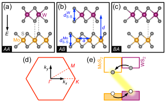
We considered WS2/MoS2 and WSe2/MoSe2 in three stacking configurations, motivated by experimental and theoretical considerations, labeled (180∘), (0∘), and (0∘), Figs. 1(a)-(c), following the convention of Ref. Constantinescu et al. (2013): specifically, is fully eclipsed; is staggered with W atoms aligned with atoms of the other layer; is staggered with Mo atoms aligned with atoms of the other layer [dashed lines in Figs. 1(a)-(c)]. Although arbitrary twist angles can be achieved by mechanical transfer, interlayer excitons generated at the valleys are direct for small angles around 0∘ and 180∘, resulting in brighter PL Yu et al. (2015b). Furthermore, CVD growth of WS2 on MoS2 resulted in stacking Gong et al. (2014); Yu et al. (2015a), while similar growth of WSe2 on MoSe2 resulted in and stackings Gong et al. (2015); He et al. (2016). We restricted ourselves to pure chalcogenide compounds ( = in W/Mo) in order to minimize strain within a commensurate, cell. When optimized, the lattice constants () of the heterobilayers deviate at most by 0.3% from the lattice constants of their constituent layers in homobilayer form. Similarly, the interlayer distances () of -W/Mo lie within 0.2% of the average between -bilayer W and -bilayer Mo. At the largest electric field considered (5 V/nm), values change by less than 0.4% of their zero-field values.
Figures 2(a)-(e) display the band structure evolution of an example heterobilayer, -WS2/MoS2, under a perpendicular electric field. High-symmetry points in the BZ are defined in Fig. 1(d). At zero field, -WS2/MoS2 exhibits an indirect gap of 1.21 eV. The conduction band minimum at originates from MoS2, whereas the valence band maximum at has sizeable contributions from WS2 and MoS2. However, the valence band at originates from WS2, resulting in a type-II band alignment at with a direct gap of 1.35 eV. We compare these results with experimental data acquired by scanning tunneling spectroscopy (STS), which probes the single-particle spectrum without excitonic effects Ugeda et al. (2014). In a recent measurement of WS2/MoS2 and MoS2/WS2 transferred onto fused quartz, the single-particle gap observed was 1.45 eV Hill et al. (2016). The MoS2 conduction band minimum was found to lie at , whereas it was experimentally uncertain whether the WS2 valence band maximum resided at or . Previous theoretical works on -WS2/MoS2, using hybrid functionals Kośmider and Fernández-Rossier (2013) or single-shot Debbichi et al. (2014), predicted gap values of 1.60 eV (direct) and 1.96 eV (indirect) respectively (none of these calculations included substrate effects, which are known to be present in the STS measurements). We note that the order of band alignments predicted by PBE and agree with each other Liang et al. (2013).
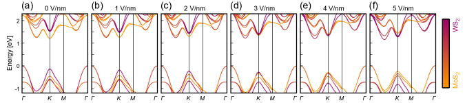
As the electric field increases [in the direction shown in Fig. 1(a)], there are various non-rigid transformations in the band structure, such as the shifting of the conduction band minimum from to a midway point along . The primary feature of interest for our purposes is the band alignment at , which becomes inverted beyond 4 V/nm [Fig. 2(e)], as well as the possible hybridization of bands at these crossings. We hereafter focus on the point, where direct transitions result in bright PL signals Yu et al. (2015b) and interlayer excitons exhibit valley-polarized dynamics Rivera et al. (2016).
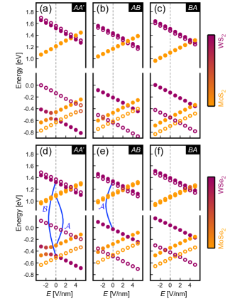
Figure 3 shows the evolution of valence and conduction bands at across a range of positive and negative electric fields, for all six heterobilayers considered. Away from crossings, the energies of W-derived bands decrease linearly with electric field, while the energies of Mo-derived bands increase linearly with electric field.
These results show clearly several important trends:
(i) Electrostatic inversion of the type-II band alignment is possible, but requires large fields. The -stacked heterobilayers have the smallest critical fields, which are 3.0 V/nm for WS2/MoS2 and 3.1 V/nm for WSe2/MoSe2, based on linear fits to the spin-up bands.
(ii) The magnitudes of the slopes of the band energies versus field decrease in the order of MoS2-, and MoSe2-derived bands. This trend is partly due to the greater polarizability of Se over S.
(iii) The distinction between and stacking being whether the W or Mo atoms are aligned with the atoms of the opposite layer, these two registries produce net dipole moments at zero field pointing in opposite directions. Thus, to first order, the plots are horizontal shifts of the plots by 1.7 V/nm for WS2/MoS2 and 1.4 V/nm for WSe2/MoSe2.
(iv) Away from crossings, the spin splittings remain relatively constant, and are larger in magnitude for heavier elements.
(v) There is a sizeable hybridization between valence bands of same spin in the heterobilayers. Smaller hybridizations can also occur when opposite-spin bands cross [for example, in Figs. 3(b) and (f)], but they are more difficult to observe due to our discrete sampling of electric field values.
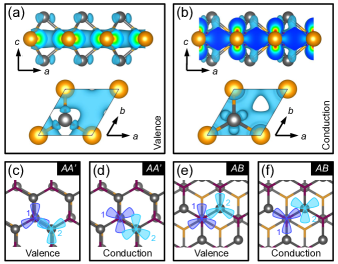
To elucidate the origin of these effects, we consider the wave functions in the monolayer limit. Figures 4(a) and (b) show the charge density isosurfaces of the valence and conduction band states at in a monolayer of MoS2. Near the S atom, the valence band state has lobes directed along the bonds, whereas the conduction band state has lobes directed between the bonds. Based on Wannier transformations of DFT calculations Fang et al. (2015), the state at the valence band maximum can be decomposed into -like orbitals on the Mo atom and -like orbitals on the S atoms. Similarly, the state at the conduction band minimum can be decomposed into -like orbitals on the Mo atom and -like orbitals on the S atoms. These states at have symmetry (threefold rotation): under a counterclockwise rotation of 120∘ about the S atom, they acquire phase factors of , where for the valence and conduction bands, respectively.
Generalizing to heterobilayers, we note that for , , and stacking configurations, crystalline symmetry is maintained about each atomic site, and is unaffected by a perpendicular electric field. Thus, for states located on opposite layers to hybridize, their wave functions must transform with the same phase factor under threefold rotation. For a given state, counterclockwise rotation of 120∘ about a fixed atomic site engenders a phase factor of , where
| (1) |
The first term represents a Bloch phase, where and is a displacement vector of the atom that may arise from rotation. The second term, which was introduced in the previous paragraph, is generated by orbital angular momentum, with being the valley index. We note that for the 180∘-oriented WX2 layer in the heterobilayers, and otherwise. The third term is due to spin, with for spins pointing in the positive/negative direction. Using Eq. 1, we derive a set of hybridizations permitted by symmetry, shown in Table S1. The actual strength of hybridization depends on matrix elements of the electric field operator, and appears to be greatest in the valence bands of heterobilayers. The stronger hybridization of these states could be due to a greater overlap of the charge densities near the atoms facing the interlayer cavity [Figs. 4(c)-(f)].
| W/Mo | W/Mo | W/Mo | |
|---|---|---|---|
| W/Mo | |||
| W/Mo | W/Mo | W/Mo |
In what concerns direct excitons at , our results imply that in the 0∘-stacked heterobilayers, the offset between the spin-up conduction bands defines an upper bound on the binding energy of interlayer excitons relative to that of the intralayer, W exciton Rivera et al. (2015) [see Fig. 3(e)]. The actual binding energy of interlayer excitons is reduced due to the weaker Coulomb interaction between their spatially-separated charges, and vary depending on fabrication details Tongay et al. (2014); Gong et al. (2014); Yu et al. (2015a). Our results suggest that these energies can be tuned in two ways: First, by shifting the stacking registry from to , the spin-up, conduction band offset increases from 0.27 eV to 0.41 eV in WS2/MoS2 and from 0.23 eV to 0.34 eV in WSe2/MoSe2 (DFT total energies for the and stackings are degenerate within 1 meV, suggesting that the configurations are equally stable). Second, by applying electric fields up to V/nm, which are attainable in experiments involving dual-gated devices Chu et al. (2015), the spin-up, conduction band offsets vary on average by eV in WS2/MoS2 and eV in WSe2/MoSe2.
In the 180∘-stacked heterobilayers, the large hybridization of valence bands at should in principle affect the intralayer, W exciton and the intralayer, Mo exciton [see Fig. 3(d)]. At zero field, the W exciton can dissociate due to charge transfer from the spin-up W bands to the spin-up Mo bands, so its PL signal may already be quenched. However, the Mo exciton cannot dissociate by hole transfer onto W without a spin flip, which is expected to occur rarely Rivera et al. (2016); thus, its PL signal should be observable. As the system is tuned towards the hybridization point (near V/nm for WS2/MoS2), we expect the recombination rate of the Mo exciton to drop. This is due to the hole sector of the excitonic wave function becoming spread over both layers, reducing its overlap with the electron sector that is confined to the Mo layer Chu et al. (2015). Thus, valence band hybridization should lead to an observable darkening of the Mo exciton.
In summary, we report two effects of the stacking configuration that have impact on optoelectronic properties of W/Mo TMDC heterobilayers: First, relative shifts in the stacking registry can induce different net dipole moments, leading to band offset variations that affect the binding energy of interlayer excitons. Second, depending on the stacking configuration, a perpendicular electric field may hybridize W and Mo bands that cross at , darkening the intralayer excitons associated with these bands. We expect that these stacking effects may be enriched upon introduction of small twist angles about 0∘ or 180∘.
Acknowledgements.
We thank S. Fang and L. A. Jauregui for helpful discussions. Computations were performed on the Odyssey cluster supported by the FAS Division of Science, Research Computing Group at Harvard University. Atomic structures and charge density plots were produced using VESTA Momma and Izumi (2011). We acknowledge support from Army Research Office (ARO-MURI) W911NF-14-1-0247.Supplemental Material
.1 Structural features of heterobilayers
We summarize the calculated structural features of the relaxed heterobilayers in Table S1.
| WS2/MoS2 | WSe2/MoSe2 | |||||
|---|---|---|---|---|---|---|
| [Å] | 3.16 | 3.17 | 3.17 | 3.30 | 3.30 | 3.30 |
| [Å] | 6.13 | 6.06 | 6.08 | 6.47 | 6.45 | 6.47 |
| [Å] | 3.13 | 3.12 | 3.12 | 3.34 | 3.34 | 3.34 |
| [Å] | 3.15 | 3.14 | 3.14 | 3.37 | 3.37 | 3.37 |
.2 Van der Waals correction
Due to the long-range nature () of the empirical van der Waals interaction, an especially large vacuum region within the DFT cell is required to mitigate the influence of periodic images on the TMDC heterobilayer of interest. For a 3D system, Ewald summation of the dispersion energy is both appropriate and accurate Kerber et al. (2008). However, for our 2D heterobilayer, we found that it slowed the convergence of the interlayer distance () with respect to the cell dimension along the axis [Figs. S1(a), (b)]. At large values of , the heterobilayer is still slightly pulled apart by its periodic images. To speed up convergence, we truncated the pairwise interactions beyond a cutoff radius of 25 Å.
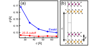
Although we strive to calculate the interlayer distance as accurately as possible, small deviations have very little effect on the band structure [Figs. S2(a), (b)], and no effect on the hybridization selection rules that are the main focus of our manuscript.

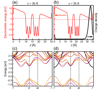
.3 Artificial vacuum states
In the implementation of a perpendicular electric field within periodic boundary conditions, a triangular potential well is necessarily created at the boundary of the DFT cell [Figs. S3(a), (b)]. This artificial potential can trap quantum well states in the vacuum, leading to the appearance of 2D, free-electron bands centered at [Figs. S3(c), (d)]. On one hand, the long-range, van der Waals interaction favors enlarging the DFT cell along the axis, as described previously. On the other hand, for a fixed electric field, the vacuum states get lowered in energy as increases, leading to difficulties in electronic relaxation if they drop below the valence band maximum. To balance this tradeoff, we took to be 35 Å. At this value, the lowest vacuum state at 5 V/nm remains well above the valence band maximum, and the band structure exhibits no change with respect to a calculation with = 30 Å. Post calculaton, we removed the vacuum states by dropping bands with negligible projections onto the Mo, W, S, and Se orbitals.
The empty vacuum states may complicate calculations, as a large number of bands (up to 1750 in monolayer MoS2 Fang et al. (2015)) are typically required for convergence. Further investigations are required to evaluate and possibly negate their influence.
Reference Ramasubramaniam et al. (2011) showed the emergence of a parabolic, band in bilayer WS2 at 2.7 V/nm, and Ref. Nguyen et al. (2016) reported a gap closing at the point in bilayer MoS2 at 5.5 V/nm. We suggest that these features may originate from artificial vacuum states.
References
- Geim and Grigorieva (2013) A. K. Geim and I. V. Grigorieva, Nature 499, 419 (2013).
- Mak et al. (2010) K. F. Mak, C. Lee, J. Hone, J. Shan, and T. F. Heinz, Phys. Rev. Lett. 105, 136805 (2010).
- Splendiani et al. (2010) A. Splendiani, L. Sun, Y. Zhang, T. Li, J. Kim, C.-Y. Chim, G. Galli, and F. Wang, Nano Lett. 10, 1271 (2010).
- Wang et al. (2012) Q. H. Wang, K. Kalantar-Zadeh, A. Kis, J. N. Coleman, and M. S. Strano, Nat. Nanotechnol. 7, 699 (2012).
- Furchi et al. (2014) M. M. Furchi, A. Pospischil, F. Libisch, J. Burgdörfer, and T. Mueller, Nano Lett. 14, 4785 (2014).
- Hong et al. (2014) X. Hong, J. Kim, S.-F. Shi, Y. Zhang, C. Jin, Y. Sun, S. Tongay, J. Wu, Y. Zhang, and F. Wang, Nat. Nanotechnol. 9, 682 (2014).
- Ceballos et al. (2014) F. Ceballos, M. Z. Bellus, H.-Y. Chiu, and H. Zhao, ACS Nano 8, 12717 (2014).
- Yu et al. (2015a) Y. Yu, S. Hu, L. Su, L. Huang, Y. Liu, Z. Jin, A. A. Purezky, D. B. Geohegan, K. W. Kim, Y. Zhang, and L. Cao, Nano Lett. 15, 486 (2015a).
- Chiu et al. (2015) M.-H. Chiu, C. Zhang, H.-W. Shiu, C.-P. Chuu, C.-H. Chen, C.-Y. S. Chang, C.-H. Chen, M.-Y. Chou, C.-K. Shih, and L.-J. Li, Nat. Commun. 6, 7666 (2015).
- Rigosi et al. (2015) A. F. Rigosi, H. M. Hill, Y. Li, A. Chernikov, and T. F. Heinz, Nano Lett. 15, 5033 (2015).
- Lee et al. (2014) C.-H. Lee, G.-h. Lee, A. M. van der Zande, W. Chen, Y. Li, M. Han, X. Cui, G. Arefe, C. Nuckolls, T. F. Heinz, J. Guo, J. Hone, and P. Kim, Nat. Nanotechnol. 9, 676 (2014).
- Fang et al. (2014) H. Fang, C. Battaglia, C. Carraro, S. Nemsak, B. Ozdol, J. S. Kang, H. A. Bechtel, S. B. Desai, F. Kronast, A. A. Unal, G. Conti, C. Conlon, G. K. Palsson, M. C. Martin, A. M. Minor, C. S. Fadley, E. Yablonovitch, R. Maboudian, and A. Javey, Proc. Natl. Acad. Sci. 111, 6198 (2014).
- Chiu et al. (2014) M.-H. Chiu, M.-Y. Li, W. Zhang, W.-T. Hsu, W.-H. Chang, M. Terrones, H. Terrones, and L.-J. Li, ACS Nano 8, 9649 (2014).
- Gong et al. (2014) Y. Gong, J. Lin, X. Wang, G. Shi, S. Lei, Z. Lin, X. Zou, G. Ye, R. Vajtai, B. I. Yakobson, H. Terrones, M. Terrones, B. K. Tay, J. Lou, S. T. Pantelides, Z. Liu, W. Zhou, and P. M. Ajayan, Nat. Mater. 13, 1135 (2014).
- Rivera et al. (2015) P. Rivera, J. R. Schaibley, A. M. Jones, J. S. Ross, S. Wu, G. Aivazian, P. Klement, K. Seyler, G. Clark, N. J. Ghimire, J. Yan, D. G. Mandrus, W. Yao, and X. Xu, Nat. Commun. 6, 6242 (2015).
- Gong et al. (2015) Y. Gong, S. Lei, G. Ye, B. Li, Y. He, K. Keyshar, X. Zhang, Q. Wang, J. Lou, Z. Liu, R. Vajtai, W. Zhou, and P. M. Ajayan, Nano Lett. 15, 6135 (2015).
- Rivera et al. (2016) P. Rivera, K. L. Seyler, H. Yu, J. R. Schaibley, J. Yan, D. G. Mandrus, W. Yao, and X. Xu, Science 351, 688 (2016).
- He et al. (2016) Y. He, Y. Yang, Z. Zhang, Y. Gong, W. Zhou, Z. Hu, G. Ye, X. Zhang, E. Bianco, S. Lei, Z. Jin, X. Zou, Y. Yang, Y. Zhang, E. Xie, J. Lou, B. Yakobson, R. Vajtai, B. Li, and P. Ajayan, Nano Lett. 16, 3314 (2016).
- Tongay et al. (2014) S. Tongay, W. Fan, J. Kang, J. Park, U. Koldemir, J. Suh, D. S. Narang, K. Liu, J. Ji, J. Li, R. Sinclair, and J. Wu, Nano Lett. 14, 3185 (2014).
- Chernikov et al. (2015) A. Chernikov, A. M. van der Zande, H. M. Hill, A. F. Rigosi, A. Velauthapillai, J. Hone, and T. F. Heinz, Phys. Rev. Lett. 115, 126802 (2015).
- Fogler et al. (2014) M. M. Fogler, L. V. Butov, and K. S. Novoselov, Nat. Commun. 5, 4555 (2014).
- Ramasubramaniam et al. (2011) A. Ramasubramaniam, D. Naveh, and E. Towe, Phys. Rev. B 84, 205325 (2011).
- Liu et al. (2012) Q. Liu, L. Li, Y. Li, Z. Gao, Z. Chen, and J. Lu, J. Phys. Chem. C 116, 21556 (2012).
- Santos and Kaxiras (2013) E. J. G. Santos and E. Kaxiras, ACS Nano 7, 10741 (2013).
- Zhang et al. (2014) Z. Y. Zhang, M. S. Si, Y. H. Wang, X. P. Gao, D. Sung, S. Hong, and J. He, J. Chem. Phys. 140, 174707 (2014).
- Xiao et al. (2014) J. Xiao, M. Long, X. Li, Q. Zhang, H. Xu, and K. Chan, J. Phys. Condens. Matter 26, 405302 (2014).
- Zibouche et al. (2014) N. Zibouche, P. Philipsen, A. Kuc, and T. Heine, Phys. Rev. B 90, 125440 (2014).
- Shanavas and Satpathy (2015) K. V. Shanavas and S. Satpathy, Phys. Rev. B 91, 235145 (2015).
- Nguyen et al. (2016) C. V. Nguyen, N. N. Hieu, and V. V. Ilyasov, J. Electron. Mater. 45, 4038 (2016).
- Lu et al. (2014) N. Lu, H. Guo, L. Li, J. Dai, L. Wang, W.-N. Mei, X. Wu, and X. C. Zeng, Nanoscale 6, 2879 (2014).
- Sharma et al. (2014) M. Sharma, A. Kumar, P. K. Ahluwalia, and R. Pandey, J. Appl. Phys. 116, 063711 (2014).
- Kresse and Furthmüller (1996a) G. Kresse and J. Furthmüller, Comp. Mater. Sci. 6, 15 (1996a).
- Kresse and Furthmüller (1996b) G. Kresse and J. Furthmüller, Phys. Rev. B 54, 11169 (1996b).
- Blöchl (1994) P. E. Blöchl, Phys. Rev. B 50, 17953 (1994).
- Kresse and Joubert (1999) G. Kresse and D. Joubert, Phys. Rev. B 59, 1758 (1999).
- Perdew et al. (1996) J. P. Perdew, K. Burke, and M. Ernzerhof, Phys. Rev. Lett. 77, 3865 (1996).
- Neugebauer and Scheffler (1992) J. Neugebauer and M. Scheffler, Phys. Rev. B 46, 16067 (1992).
- Makov and Payne (1995) G. Makov and M. C. Payne, Phys. Rev. B 51, 4014 (1995).
- Tkatchenko and Scheffler (2009) A. Tkatchenko and M. Scheffler, Phys. Rev. Lett. 102, 073005 (2009).
- Bučko et al. (2013) T. Bučko, S. Lebègue, J. Hafner, and J. G. Ángyán, Phys. Rev. B 87, 064110 (2013).
- Constantinescu et al. (2013) G. Constantinescu, A. Kuc, and T. Heine, Phys. Rev. Lett. 111, 036104 (2013).
- Yu et al. (2015b) H. Yu, Y. Wang, Q. Tong, X. Xu, and W. Yao, Phys. Rev. Lett. 115, 187002 (2015b).
- Ugeda et al. (2014) M. M. Ugeda, A. J. Bradley, S.-F. Shi, F. H. da Jornada, Y. Zhang, D. Y. Qiu, W. Ruan, S.-K. Mo, Z. Hussain, Z.-X. Shen, F. Wang, S. G. Louie, and M. F. Crommie, Nat. Mater. 13, 1091 (2014).
- Hill et al. (2016) H. M. Hill, A. F. Rigosi, K. T. Rim, G. W. Flynn, and T. F. Heinz, Nano Lett. 16, 4831 (2016).
- Kośmider and Fernández-Rossier (2013) K. Kośmider and J. Fernández-Rossier, Phys. Rev. B 87, 075451 (2013).
- Debbichi et al. (2014) L. Debbichi, O. Eriksson, and S. Lebègue, Phys. Rev. B 89, 205311 (2014).
- Liang et al. (2013) Y. Liang, S. Huang, R. Soklaski, and L. Yang, Appl. Phys. Lett. 103, 042106 (2013).
- Fang et al. (2015) S. Fang, R. Kuate Defo, S. N. Shirodkar, S. Lieu, G. A. Tritsaris, and E. Kaxiras, Phys. Rev. B 92, 205108 (2015).
- Chu et al. (2015) T. Chu, H. Ilatikhameneh, G. Klimeck, R. Rahman, and Z. Chen, Nano Lett. 15, 8000 (2015).
- Momma and Izumi (2011) K. Momma and F. Izumi, J. Appl. Crystallogr. 44, 1272 (2011).
- Kerber et al. (2008) T. Kerber, M. Sierka, and J. Sauer, J. Comput. Chem. 29, 2088 (2008).