Effects of Interlayer Coupling on Hot Carrier Dynamics
in Graphene-derived van der Waals Heterostructures
Abstract
Graphene exhibits promise as a plasmonic material with high mode confinement that could enable efficient hot carrier extraction. We investigate the lifetimes and mean free paths of energetic carriers in free-standing graphene, graphite and a heterostructure consisting of alternating graphene and hexagonal boron nitride layers using ab initio calculations of electron-electron and electron-phonon scattering in these materials. We find that the extremely high lifetimes (3 ps) of low-energy carriers near the Dirac point in graphene, which are a hundred times larger than that in noble metals, are reduced by an order of magnitude due to inter-layer coupling in graphite, but enhanced in the heterostructure due to phonon mode clamping. However, these lifetimes drop precipitously with increasing carrier energy, and are smaller than those in noble metals at energies exceeding 0.5 eV. By analysing the contribution of different scattering mechanisms and inter-layer interactions, we identify desirable spacer layer characteristics – high dielectric constant and heavy atoms – that could pave the way for plasmonic heterostructures with improved hot carrier transport.
Two-dimensional (2D) materials exhibit a diverse array of optical and electronic properties, ranging from insulating hexagonal boron nitride and semiconducting transition metal dichalcogenides to semimetallic graphene.Castro Neto et al. (2009); Novoselov et al. (2004); Geim and Novoselov (2007); R. et al. (2010); Giovannetti et al. (2007) Stacked 2D materials, or van der Waals (vdW) heterostructures,Xia et al. (2014); Geim and Grigorieva (2013); Jariwala et al. (2016) have generated considerable recent interest as designer plasmonic, photonic and optoelectronic materials. Combining 2D layers in different arrangements makes it possible to realize a variety of new optical phenomena and nanophotonic devices, covering spectral ranges from the microwave to the ultraviolet.Ci et al. (2010); Jablan et al. (2009); Bonaccorso et al. (2010)
Simultaneously, the field of utilizing the energetic ‘hot’ carriers generated by surface plasmon decay for photodetection and solar energy conversion has grown rapidly.Brongersma et al. (2015); Narang et al. (2016); Xia et al. (2009) Hot carrier extraction has also been demonstrated in graphene,Oum et al. (2014); Winnerl et al. (2011) with experimental techniques such as pump-probe spectroscopyNorris et al. (2003) and four-dimensional electron microscopyZewail (2010); van der Veen et al. (2015) used to explore the energy relaxation dynamics.Breusing et al. (2009); Carbone et al. (2011) However, these techniques conventionally provide indirect signatures of the response of a large number of thermalizing carriers,Butscher et al. (2007) and extensive theoretical modeling is necessary to extract information about the sub-picosecond non-equilibrium carrier dynamics of interest.Tielrooij et al. (2013)
With an ab initio framework for calculating optical response and electron-phonon interactions, we previously evaluated mechanisms of hot carrier generation and relaxation in plasmonic metals,Sundararaman et al. (2014); Brown et al. (2016a) and identified their signatures in ultrafast pump-probe measurements.Brown et al. (2016b, c) In particular, the small mean free paths of higher energy carriers helped elucidate the efficiency limits in plasmonic energy conversion devices and potential strategies to overcome them.Narang et al. (2016) Here, we investigate the dynamics of hot carriers in graphene and in graphene-derived vdW heterostructures to explore their potential for efficient hot carrier extraction. The focus of previous work in carrier dynamics (that includes electron-phonon coupling in graphene) has primarily been on low-energy carriers that dominate many properties of interest such as near-equilibrium charge transport.Park et al. (2009) From a plasmonic hot carrier devices perspective, we instead focus on first principles calculations of higher energy carrier dynamics. In particular, we calculate the energy-dependent life times and mean free paths of hot carriers in free-standing graphene, and additionally to evaluate the role of inter-layer interactions, in graphite and graphene/hBN (alternating graphene and hexagonal boron-nitride layers), as shown in Fig. 1(a). Of many possible heterostructures between graphene and hBN, we pick the simplest configuration which is computationally most tractable with fewest atoms per unit cell, and captures all the relevant interactions with maximum graphene-hBN interactions.The presence of dopants to shift the Fermi level will alter the carrier dynamics and a detailed description of this interaction is not the primary focus here.Caruso and Giustino (2016)
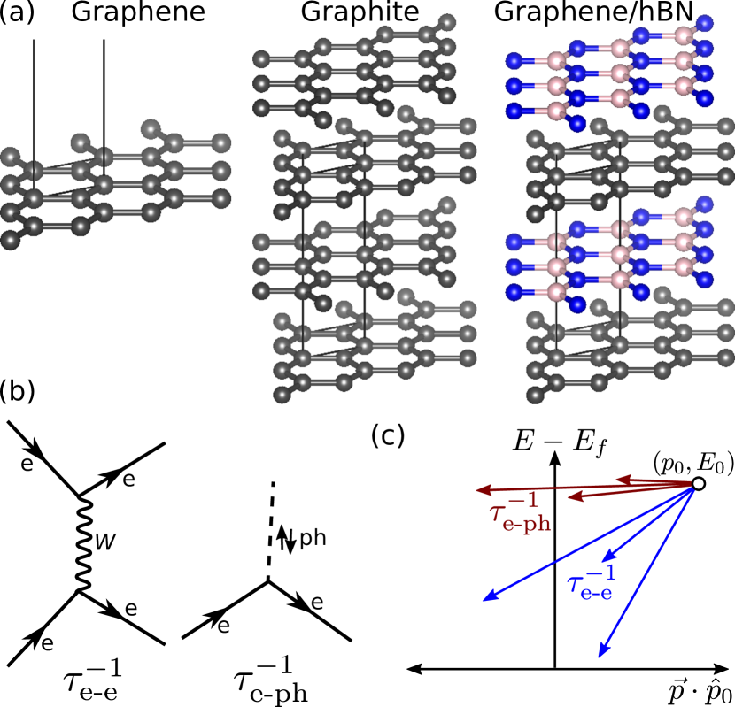
The intrinsic carrier relaxation rate in materials is determined by two prominent processes, electron-phonon (e-ph) scattering and electron-electron (e-e) scattering, as shown in Fig. 1(b). Fermi’s Golden rule for e-ph scattering yields the rateBrown et al. (2016a)
| (1) |
Above, electronic states with energies and Fermi-Dirac occupation factors are labeled by wave-vectors in the Brillouin zone BZ and band indices . Phonon states with energies and Bose-Einstein occupation factors are labelled by wave-vectors ( by momentum conservation) and polarization index . The electron-phonon matrix elements couple two electronic states with a phonon mode as in the 3-vertex shown in Fig. 1(b).
On the other hand, the rate for electron-electron scattering is given byBrown et al. (2016a); Ladstädter et al. (2004)
| (2) |
Above, the relevant matrix element for Fermi’s golden rule is obtained by the overlap of the density matrix between initial and final electronic wavefunctions, expanded in the plane-wave basis with reciprocal lattice vectors , with the imaginary part of the dynamically screened Coulomb operator . This operator is written in terms of the electronic dielectric function, which in turn, is derived from the electronic density matrices and energies. Note that the density matrices contain the lower incoming and outgoing electronic states in Fig. 1(b), while contains the virtual photon propagator and the upper electronic states. See Ref. 30 for a detailed exposition and Ref. 25 for our implementation details.
Both (1) for e-ph scattering and (2) for e-e scattering couple electrons with any incoming and outgoing wavevectors, and , and are therefore capable, in general, of completely changing the momentum direction in a single scattering event, as shown in Fig. 1(c). The energy conservation in (1) only couples incoming and outgoing electronic states differing by a phonon energy. Since phonon energies are typically eV or smaller, while relevant electronic energies are eV, e-ph scattering only relaxes a small fraction of the energy in each scattering event. In contrast, (2) couples an incoming electronic state with any outgoing electronic state with a smaller magnitude of energy,Brown et al. (2016a) so that e-e scattering relaxes the hot carrier energy much more efficiently per scattering event, as indicated in Fig. 1(c). Coupling and scattering with phonon polaritons, hyperbolic modes in hBN and super-collisions have been considered elsewhere and are not included here.Betz et al. (2012, 2013); Song et al. (2012)
We perform ab initio density-functional theory (DFT) calculations of the electronic band structure, phonon dispersion relations and electron-phonon matrix elements used in (1-2). We use maximally-localized Wannier functionsSouza et al. (2001) to interpolate all the DFT-calculated quantities from a coarser Brillouin zone mesh () to the much finer meshes (), which is critical for accurately resolving the phonon energy scales in ab initio calculations of electron-phonon properties.Brown et al. (2016a) For graphene, we use truncated Coulomb potentialsSundararaman and Arias (2013) to isolate periodic images along the third direction, and set the Brillouin zone sampling to 1 in that direction. Additionally, we use the plane-wave basis with a kinetic energy cutoff of 30 Hartrees, norm-conserving pseudopotentials,Schlipf and Gygi (2015) and the ‘PBE’ generalized-gradient approximation to the exchange-correlation functional,Perdew et al. (1996) all as implemented in our open-source DFT software, JDFTx.Sundararaman et al. (2012) See Ref. 25 for further computational and implementation details.
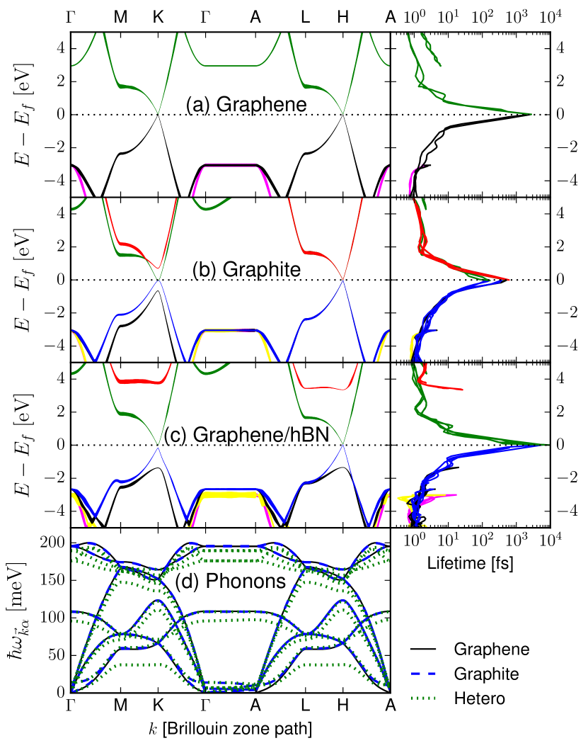
Fig. 2 shows the calculated electronic bandstructure and corresponding carrier lifetimes for graphene, graphite and graphene/hBN (the heterostructure with alternating graphene and hexagonal boron nitride layers shown in Fig. 1(c)). The shape of the vs curves in these materials is qualitatively similar to that in conventional metals.Brown et al. (2016a) For carriers close to the Fermi level, is dominated by e-ph scattering. With increasing energy, the contribution of e-e scattering increases causing a rapid drop in . The key difference between conventional metals and these materials, however, is the magnitude of the lifetimes. In particular, note that the maximum carrier lifetime in graphene (near the Fermi level) is approximately 3000 fs, almost two orders of magnitude larger than the typical maximum lifetimes of 30-40 fs in noble metals.Brown et al. (2016a)
Fig. 2 also correlates the band structure for each material with the energy dependence of the carrier lifetimes, and shows the carrier linewidth () on the band structure as well. For example, note that near the Dirac point in graphene (at the point in the Brillouin zone), the lines narrow to essentially zero width due to the orders of magnitude increase in the carrier lifetime. At approximately 2 eV below the (intrinsic) Fermi level, the carrier lifetimes are smaller by a factor of 2 – 3 in the segment compared to the segment, seen qualitatively in the thicker lines on the bandstructure near , and read quantitatively off the right panels containing the lifetimes. Specifically, this decrease in lifetime is due to the flattening of the energy vs relation near the point, which results in a higher density of states and a greater electron-phonon scattering rate. In general, the lifetime decreases mostly monotonically with increasing carrier energy away from the Fermi level, until additional bands become accessible at higher energies, for example, at approximately 3 eV above the Fermi level. These bands show up as an additional segment starting at a higher lifetime in the right panel.
In going from graphene to graphite in Fig. 2(b), the bands crossing at the Dirac point () pick up a small curvature, and additional low-lying bands appear approximately 1 eV above and below the Fermi level. However, at the point, which is directly above the point at the Brillouin zone boundary along the direction, the bands continue to cross linearly as in the Dirac point in graphene. (Intuitively, the zone-boundary implies that the wavefunctions are out of phase between the two graphene layers in the graphite unit cell, which minimizes the effect of wavefunction overlaps between the two layers on the band energies at that point.) Correspondingly, in the lifetime panel, there are two branches: a higher lifetime branch corresponding to the point vicinity, and lower lifetime branch corresponding to the point. Even the higher of the two lifetimes at the Fermi level is approximately 600 fs, an order of magnitude lower than in graphene, because of the increased phase space for electron-phonon scattering due to the aforementioned band curvature at the point.
Next, Fig. 2(c) shows that separating graphene layers with hexagonal boron nitride layers preserves the graphene band structure near the Dirac point, and restores the high maximum carrier lifetimes of graphene. This is because, unlike in graphite, the bands of the insulating boron nitride are far from the Fermi level and do not hybridize with the graphene bands near the Fermi level. In fact, the maximum carrier lifetimes in the graphene/hBN heterostructure exceed that of free-standing graphene because adjacent layers clamp down the out-of-plane vibrations of the atoms, increasing the corresponding -polarized acoustic (‘ZA’) phonon frequencies, thereby reducing the corresponding phonon occupation factors and the electron-phonon scattering rates in (1).
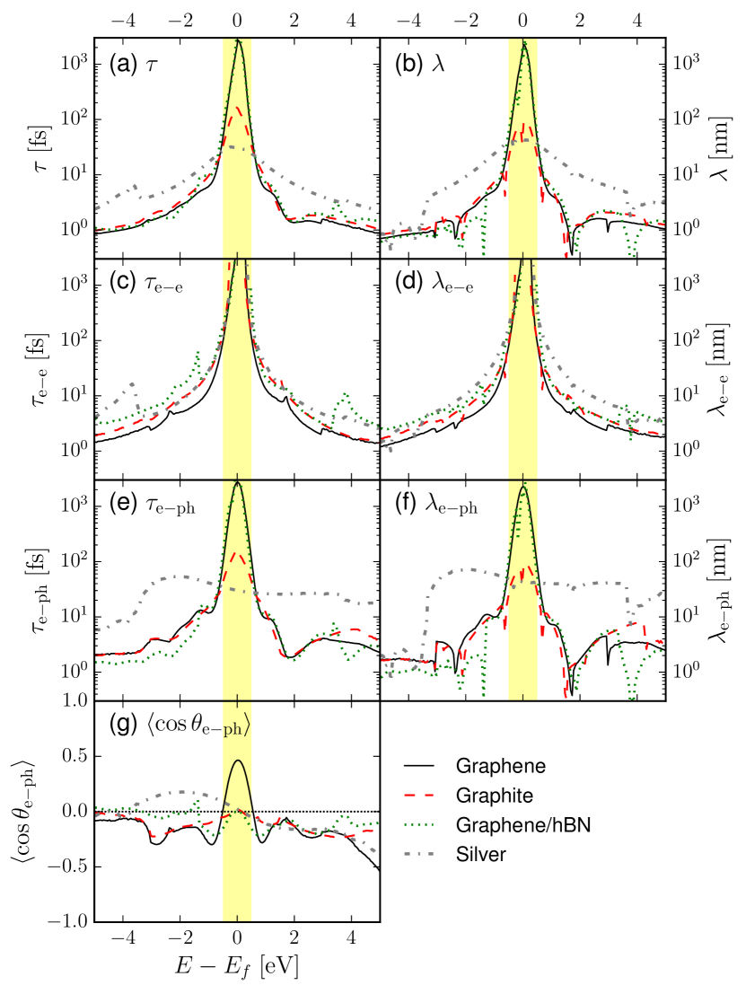
Finally, Fig. 3 compares the total values and individual contributions of e-e and e-ph scattering to the lifetime and mean free path (where the carrier group velocity is also calculated from the band structure in the Wannier representation). To make the comparisons between different materials clear, we now plot a single value for each quantity as a function of energy, averaging out the anisotropic -dependence previously shown in Fig. 2. The top two panels, Fig. 3(a,b), show as before that graphene and graphene/hBN have the highest Fermi level and , with the corresponding values in graphite one order of magnitude smaller. In comparison, the peak values for silver are fs and nm, which are an additional order of magnitude smaller than the graphite case. Therefore, the 2D materials are clearly superior for transport of low-energy carriers, as is established in previous studies.Kim et al. (2011); Park et al. (2008); Nomura and MacDonald (2007); Hwang et al. (2007)
Importantly, however, the lifetimes and mean free paths of the 2D materials decreases with carrier energy magnitude much faster than in the case of noble metals like silver. Consequently, outside the energy window extending 0.5 eV above and below the Fermi level highlighted in Fig. 3, and are larger in silver than they are for any of the 2D materials, by almost a factor of for eV carriers. Panels (c) and (d) of Fig. 3 show that e-e scattering at higher energies is somewhat comparable between the graphene-derived vdW heterostructures and silver. Instead, panels (e) and (f) show that the dramatic reduction of higher-energy in the graphene-derived vdW heterostructures is due to increased e-ph scattering, which in turn is attributable to softer phonon modes and stronger electron-phonon coupling with the lighter atoms.
Comparisons of the e-e and e-ph contributions between the graphene-derived vdW heterostructures in Fig. 3(c) and (e) reveal an interesting competition. The e-e scattering rate at higher carrier energies is highest in graphene, and is reduced in graphite and graphene/hBN (i.e. is increased) because the neighboring layers contribute in screening the Coulomb interaction between the electrons and therefore reduce the magnitude of in (2). On the other hand, the e-ph scattering rate at higher carrier energies is lowest in graphene, while the neighboring layers provide additional phonon modes that the electrons can scatter against thereby increasing the scattering rate (reducing ). Therefore, the ideal heterostructure for maximizing the carrier lifetimes would use spacer layers with a high-dielectric constant for optimal screening, which are rigid and consist of heavier atoms to reduce the phonon losses.
The shapes and magnitudes of corresponding and panels are peripherally very similar, because, coincidentally the typical Fermi velocity in all the materials considered here is nm/fs, but there are important differences. In particular, note the sharp increase in of silver 3.5 eV below the Fermi level in Fig. 3(c), which is due to additional bands (the bands) becoming accessible at that energy. However, those new bands have much lower group velocities, and therefore this increase is absent in the corresponding curve for silver in Fig. 3(d). Importantly, this implies that it is easier to find longer-lived (high ) high-energy carriers, than to find easy-to-collect (high ) carriers.
In addition to the scattering rate, an additional factor that affects charge transport is the change in angle upon scattering, shown in Fig. 3(g). Here would imply exclusive forward scattering and , exclusive back scattering. Most of the materials exhibit near zero over a large energy range, implying that the initial and final electron momentum directions are uncorrelated on average. The only exception is graphene near the Dirac point, where , indicating that momentum relaxation is slower by a factor of two than would indicate. Correspondingly, the mobility of free-standing graphene compared to the other materials would be a factor of two larger than that inferred by a ratio of .
By investigating electron-electron and electron-phonon scattering dynamics using a parameter-free ab initio framework that fully accounts for detalied electronic structure and phononic properties of the materials, we have identified an important avenue for 2D heterostructure research: designing materials with superior high-energy carrier transport properties. In particular, simultaneously screening electron-electron interactions and minimizing phonon losses, perhaps by combining light semi-metals (like graphene) with heavier and rigid dielectrics (such as NbTe), could enhance hot carrier transport distances. Simultaneously, the developed computational framework can be applied to quantitatively analyse ultrafast pump-probe and electron microscopy measurements and evaluate additional loss mechanisms due to defects and experimental non-idealities.
We acknowledge financial support from NG NEXT at the Northrop Grumman Corporation. PN acknowledges support from the Harvard University Center for the Environment (HUCE). Calculations were performed on the BlueGene/Q supercomputer in the Center for Computational Innovations (CCI) at Rensselaer Polytechnic Institute and calculations in this work used the National Energy Research Scientific Computing Center, a DOE Office of Science User Facility supported by the Office of Science of the U.S. Department of Energy under Contract No. DE-AC02-05CH11231.
References
- Castro Neto et al. (2009) A. H. Castro Neto, F. Guinea, N. M. R. Peres, K. S. Novoselov, and A. K. Geim, Rev. Mod. Phys. 81, 109 (2009).
- Novoselov et al. (2004) K. S. Novoselov, A. K. Geim, S. V. Morozov, D. Jiang, Y. Zhang, S. V. Dubonos, I. V. Grigorieva, and A. A. Firsov, Science 306, 666 (2004).
- Geim and Novoselov (2007) A. K. Geim and K. S. Novoselov, Nat Mater 6, 183 (2007).
- R. et al. (2010) D. R., Y. F., MericI., LeeC., WangL., SorgenfreiS., WatanabeK., TaniguchiT., KimP., S. L., and HoneJ., Nat Nano 5, 722 (2010).
- Giovannetti et al. (2007) G. Giovannetti, P. A. Khomyakov, G. Brocks, P. J. Kelly, and J. van den Brink, Phys. Rev. B 76, 073103 (2007).
- Xia et al. (2014) F. Xia, H. Wang, D. Xiao, M. Dubey, and A. Ramasubramaniam, Nat Photon 8, 899 (2014).
- Geim and Grigorieva (2013) A. K. Geim and I. V. Grigorieva, Nature 499, 419 (2013).
- Jariwala et al. (2016) D. Jariwala, T. J. Marks, and M. C. Hersam, Nat Mater advance online publication, (2016).
- Ci et al. (2010) L. Ci, L. Song, C. Jin, D. Jariwala, D. Wu, Y. Li, A. Srivastava, Z. F. Wang, K. Storr, L. Balicas, F. Liu, and P. M. Ajayan, Nat Mater 9, 430 (2010).
- Jablan et al. (2009) M. Jablan, H. Buljan, and M. Soljačić, Phys. Rev. B 80, 245435 (2009).
- Bonaccorso et al. (2010) F. Bonaccorso, Z. Sun, T. Hasan, and A. C. Ferrari, Nat Photon 4, 611 (2010).
- Brongersma et al. (2015) M. L. Brongersma, N. J. Halas, and P. Nordlander, Nat Nano 10, 25 (2015).
- Narang et al. (2016) P. Narang, R. Sundararaman, and H. A. Atwater, Nanophotonics 5, 96 (2016).
- Xia et al. (2009) F. Xia, T. Mueller, Y.-m. Lin, A. Valdes-Garcia, and P. Avouris, Nat Nano 4, 839 (2009).
- Oum et al. (2014) K. Oum, T. Lenzer, M. Scholz, D. Y. Jung, O. Sul, B. J. Cho, J. Lange, and A. Müller, The Journal of Physical Chemistry C, The Journal of Physical Chemistry C 118, 6454 (2014).
- Winnerl et al. (2011) S. Winnerl, M. Orlita, P. Plochocka, P. Kossacki, M. Potemski, T. Winzer, E. Malic, A. Knorr, M. Sprinkle, C. Berger, W. A. de Heer, H. Schneider, and M. Helm, Phys. Rev. Lett. 107, 237401 (2011).
- Norris et al. (2003) P. M. Norris, A. P. Caffrey, R. J. Stevens, J. M. Klopf, J. T. McLeskey, and A. N. Smith, Review of Scientific Instruments 74, 400 (2003).
- Zewail (2010) A. H. Zewail, Science 328, 187 (2010).
- van der Veen et al. (2015) R. M. van der Veen, T. J. Penfold, and A. H. Zewail, Structural Dynamics 2, 024302 (2015).
- Breusing et al. (2009) M. Breusing, C. Ropers, and T. Elsaesser, Phys. Rev. Lett. 102, 086809 (2009).
- Carbone et al. (2011) F. Carbone, G. Aubock, A. Cannizzo, F. V. Mourik, R. Nair, A. Geim, K. Novoselov, and M. Chergui, Chemical Physics Letters 504, 37 (2011).
- Butscher et al. (2007) S. Butscher, F. Milde, M. Hirtschulz, E. Malić, and A. Knorr, Applied Physics Letters 91, 203103 (2007).
- Tielrooij et al. (2013) K. J. Tielrooij, J. C. W. Song, S. A. Jensen, A. Centeno, A. Pesquera, A. Zurutuza Elorza, M. Bonn, L. S. Levitov, and F. H. L. Koppens, Nat Phys 9, 248 (2013).
- Sundararaman et al. (2014) R. Sundararaman, P. Narang, A. S. Jermyn, W. A. Goddard III, and H. A. Atwater, Nat. Commun. 5, 12 (2014).
- Brown et al. (2016a) A. Brown, R. Sundararaman, P. Narang, W. A. Goddard III, and H. A. Atwater, ACS Nano 10, 957 (2016a).
- Brown et al. (2016b) A. M. Brown, R. Sundararaman, P. Narang, W. A. Goddard III, and H. A. Atwater, Phys. Rev. B 94, 075120 (2016b).
- Brown et al. (2016c) A. M. Brown, R. Sundararaman, P. Narang, A. Schwartzberg, W. A. Goddard III, and H. A. Atwater, “Experimental and ab initio ultrafast carrier dynamics in plasmonic nanoparticles,” (2016c), preprint arXiv:1608.03309.
- Park et al. (2009) C.-H. Park, F. Giustino, C. D. Spataru, M. L. Cohen, and S. G. Louie, Phys. Rev. Lett. 102, 076803 (2009).
- Caruso and Giustino (2016) F. Caruso and F. Giustino, Phys. Rev. B 94, 115208 (2016).
- Ladstädter et al. (2004) F. Ladstädter, U. Hohenester, P. Puschnig, and C. Ambrosch-Draxl, Phys. Rev. B 70, 235125 (2004).
- Betz et al. (2012) A. C. Betz, F. Vialla, D. Brunel, C. Voisin, M. Picher, A. Cavanna, A. Madouri, G. Fève, J.-M. Berroir, B. Plaçais, and E. Pallecchi, Phys. Rev. Lett. 109, 056805 (2012).
- Betz et al. (2013) A. C. Betz, S. H. Jhang, E. Pallecchi, R. Ferreira, G. Feve, J.-M. Berroir, and B. Placais, Nat Phys 9, 109 (2013).
- Song et al. (2012) J. C. W. Song, M. Y. Reizer, and L. S. Levitov, Phys. Rev. Lett. 109, 106602 (2012).
- Souza et al. (2001) I. Souza, N. Marzari, and D. Vanderbilt, Phys. Rev. B 65, 035109 (2001).
- Sundararaman and Arias (2013) R. Sundararaman and T. Arias, Phys. Rev. B 87, 165122 (2013).
- Schlipf and Gygi (2015) M. Schlipf and F. Gygi, Comput. Phys. Commun. 196, 36 (2015).
- Perdew et al. (1996) J. P. Perdew, K. Burke, and M. Ernzerhof, Phys. Rev. Lett. 77, 3865 (1996).
- Sundararaman et al. (2012) R. Sundararaman, D. Gunceler, K. Letchworth-Weaver, K. A. Schwarz, and T. A. Arias, “JDFTx,” http://jdftx.sourceforge.net (2012).
- Kim et al. (2011) R. Kim, V. Perebeinos, and P. Avouris, Phys. Rev. B 84, 075449 (2011).
- Park et al. (2008) C.-H. Park, L. Yang, Y.-W. Son, M. L. Cohen, and S. G. Louie, Nat Phys 4, 213 (2008).
- Nomura and MacDonald (2007) K. Nomura and A. H. MacDonald, Phys. Rev. Lett. 98, 076602 (2007).
- Hwang et al. (2007) E. H. Hwang, S. Adam, and S. D. Sarma, Phys. Rev. Lett. 98, 186806 (2007).