Ion irradiated nano-meanders for superconducting single photon detectors
Abstract
We report the fabrication of few hundred microns long, hundreds of nanometers wide and 30 nm thick meanders made of . Thin films protected by a 8 nm-thick cap layer have been patterned by high energy (a few tens of keV) oxygen ion irradiation through photoresist masks. DC and RF characterizations outline good superconducting properties of nano-meanders that could be used as Superconducting Single Photon Detectors (SSPD). By mean of a resonant method, their inductance, which mainly sets the maximum speed of these devices, has been measured on a wide range of temperature. It compares favorably to expected values calculated from the geometry of the meanders and the known London penetration depth in .
Optical quantum information technologies (such as Quantum Key Distribution), low-light level depth imaging, space-to-ground communications, atmospheric remote sensing Hadfield1 require high efficiency infrared detectors with an ultimate sensitivity down to the single photon level as well as excellent time resolution. The first proof-of-concept of a single-photon detection mechanism occurring when a photon is absorbed by a superconducting nanowire biased close to its critical current Goltsman has generated real excitement in the community in the last decade. Superconducting long, narrow and thin meanders inserted in a read-out line are the basic building blocks of this new kind of detectors called Superconducting Single Photon Detectors (SSPD). Considerable efforts have been put forth to improve significantly their performances Hadfield until overcoming in many ways their semiconductors based counterparts. SSPD are nowadays commercially available, based on low materials such as NbN, NbTi or WSi.

Despite tremendous advantages offered by those detectors such as high quantum efficiency ( 93 at around 1.54 m) Marsili1 , high operating frequency ( 1 GHz Rosfjord ), low intrinsic dark count rate ( 0.1 cps Shibata ), low jitter (18 ps full width at half maximum You ) and broad spectral range (from visible to mid-infrared 10.6 m) Marsili ; Korneev , the operating temperature well below 4K for optimal performances prevents large scale applications of these detectors. The fabrication of based SSPD would then provide two main benefits : the ability of working at higher temperature, reducing thus drastically the cryogenic operating costs, and at higher frequency operation due to very short relaxation times Lindgren . implementation suffers from the main difficulty of preserving pristine superconducting properties during the nano-patterning process, because of defects creation or oxygen out-diffusion. Recently Arpaia et al. reported on the fabrication of / tens of microns long nanowires with a 100x50 cross section ArpaiaH of Arpaia , and /AuArpaiaI hundred of nanometers long ones with a cross section down to 50x50 , while preserving superconducting properties. The longest one in a meander shape (430 long) was 1 m wide on a 12 nm thick film. Small degradations were observed, as the critical temperature was lowered down to 70 K only Zbinden . However, no report of long and narrower meander on thin films has been made up to now.
In this work, we report on a technique that allows making hundred of microns long nano-meanders with a width down to 100 nm from ion-irradiated 30 nm-thick films. DC and RF characterizations of meander-shaped nanowires evidence good superconducting properties that are reproducible and stable in time. The inductance of the devices, a key parameter that governs the reset time /RL of an SSPD ( is the load resistance of the circuit), has been measured. Its value and its temperature dependence given by the London penetration depth one, agree very well with the expected ones in .
The fabrication method used here relies on the high sensitivity to disorder of the d-wave superconducting order parameter of High Temperature Superconducting (HTS) materials. Irradiation with high-energy oxygen ions accelerated under a few tens of kV, generates punctual defects in the crystal structure that increase the normal resistivity and reduce . A superconducting-insulating transition can be induced by increasing the defect density beyond a threshold. Superconducting devices can be designed by irradiating a thin film through a thick resist template patterned either by optical or e-beam lithography bergeal ; bergealjap . The exposed areas become insulating while the areas protected by the resist remain superconducting. The method was successfully applied to design Josephson TeraHertz Heterodyne detectors malnouapl ; malnoujap ; sharafiev and Superconducting Quantum Interference Filters ouanani made from commercial Ceraco ceraco thin films.
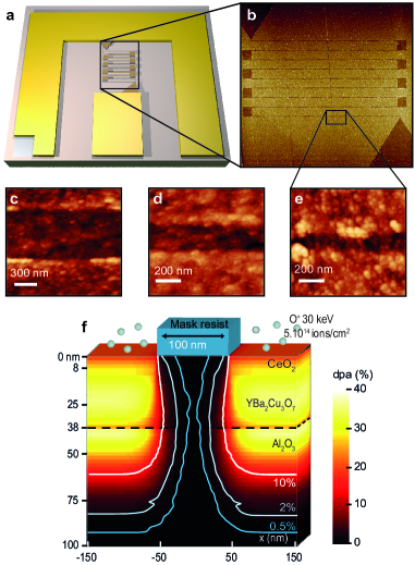
For this study, we used 30 nm-thick YBCO commercial thin films grown on a sapphire substrate and capped with a 8nm-thick layer, processed as follows. A 50 Coplanar Waveguide (CPW) line is first designed on top of the layer by e-beam lithography (Figure 1 a). The unprotected layer is removed by a 500 eV Ion Beam Etching (IBE) step, and an in-situ gold layer is deposited to form the CPW line, in good electrical contact with . Then the meander is patterned with a second e-beam lithography in a ma-N negative resist on top of the protecting layer left at the end of the CPW line. Finally, a 30 keV oxygen ion irradiation at a dose of 5 at/ through the photoresist mask defines the nano-meander by insulating its edges from the rest of the CPW line, which is itself protected by the gold layer.
The main advantages of this method is that the HTS nanowire is totally encapsulated between the insulating film on the side and the layer on the top, preventing oxygen loss. The energy and the fluence of oxygen ions necessary to make insulating without altering the nanowire have been optimized through numerical simulation using the Monte Carlo based code TRIM SRIM . This is illustrated for the 100 nm wide meander in Figure 1f, by a color-plot of the calculated local displacement per atoms (dpa) which quantifies the defect density. For dpa , the material is insulating (white line).

.
We made wires with length ranging from 20 m to 750 m and width from 100 nm to 750 nm, folded into a 8080 m2 square. Each nanowire is inserted in the central part of the CPW line (Figure 1a).The sample is connected via a PC-board, and mounted onto a cold sample holder in a cryogen-free cryostat. The DC Resistance versus Temperature (R-T) and the Current versus Voltage (I-V) curves are recorded through four probes measurements. RF measurements are performed through semi-rigid co-axial wires. It’s worth mentioning that the devices have been thermally cycled and measured several times during more than two years, with no change in their characteristics whatsoever. In this paper, we report specifically on three nano-meanders whose dimensions are 750 nm 750 m, 200 nm 450 m and 100 nm 450 m respectively. We checked that the actual widths of the conducting channels correspond to the designed ones by making Atomic Force Microscopy (AFM) images (Figure 1 b to e), thanks to a tiny swelling of the layer under irradiation ( in height). The origin of such a swelling, already reported in the literature Hurand , is not fully established yet : it is probably related to partial amorphization of the film/substrate system.
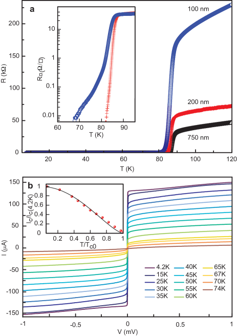
In Figure 2a, R-T curves are reported for the nano-meanders. The 750 nm wide nanowire has a midpoint critical temperature of 86 K (defined as a 50 resistance drop), identical to the one of the unprocessed film. is decreased down to 83 K and 81 K for the 200 nm and the 100 nm wide ones respectively. This can be understood in the frame of TRIM calculations, creation of defects under irradiation, as shown in Figure 1f. Indeed, ions mainly penetrate in the unprotected areas, but some are scattered, penetrate under the protected area over a mean distance of 25 nm in our case, and produce a small amount of defects (dpa). We can calculate the corresponding bulk reduction, as for instance reported in Figure 1f by the light blue (dpa = 2%) and blue (dpa = 0.5%) lines, namely a reduction of 30% and 10 % respectively. The local in the actual nanostructure is more complex to evaluate, but is certainly between these values and the one for a pristine sample, and follows the trend : the narrower the wire, the lower , as we measure. In addition, the lateral gradient in defect density induces a gradient in local , and therefore a broader resistive transition in temperature. We observed experimentally this effect as shown in inset of Figure 2 a, which is a zoom of the main part for the narrower wires. The 100 nm wire R-T transition extends over , as compared to only for the 200 nm wide one. In addition, a characteristic ”foot” in the transition is seen in the former. Then corresponds to the temperature where the resistance reaches zero with the usual criteria of an electric field of within the sample equivalent to a resistance per square of . is and for the 100 nm and 200 nm wide wires respectively.
The I-V characteristics of the 100 nm wide nanowire is presented in Figure 2 b for temperatures ranging from 4.2 K to 74 K. The critical current density is A. at 4.2 K. This value is comparable with the ones reported for nanowires Rauch ; Arpaia ; Nawaz , and is only two orders of magnitude smaller than the depairing limit . Its temperature dependence follows the Ginzburg-Landau expression generalised by Bardeen for dirty superconductors Bardeen over the whole range in temperature (inset 2 b) : with as previously measured. DC measurements highlight that our technique provides a reliable way to engineer long, narrow and thin superconducting meanders in thin films.

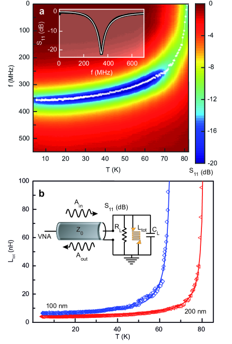
Detection events in SSPD devices generate a voltage pulse whose characteristic times are dominated by the ratio /RL, where is the inductance and the load resistance of the circuit. We designed a set-up to measure the inductance of the meanders in the low GHz frequency range. In a microwave circuit, the reflection coefficient S11 at a discontinuity between a transmission line and a load circuit is given by : , where Z0 = 50 is the characteristic impedance of the transmission line and ZL is the load impedance. In this experiment, a lumped element resonant circuit involving the nano-meander is directly connected to the CPW line (inset figure 3 b) , and the reflection coefficient S11 is measured using a Vector Network Analyser (VNA). The device is connected in parallel with a 24 pF Surface Mounted Device (SMD) capacitor and a SMD resistor , both located close to the nanowire to minimise parasitic inductances and capacitances. The nanowire acts as the inductor of a parallel RLC circuit whose impedance is :
| (1) |
The total inductance is the sum of a geometric term LG and a kinetic term LK due to the inertia of Cooper pairs in the superconducting state. At the resonant frequency, the circuit impedance is purely real . The microwave power is dissipated in the load circuit and a dip is expected in . Figure 3 a shows a color-plot of S11 as a function of frequency and temperature for the 200 nm wide meander. An absorption dip is evidenced (down to - 20 dB), at a resonant frequency f0 which strongly decreases with temperature. We fitted the data for each temperature (see for instance the 30 K trace in the inset Figure 3 a) with fixed values , the SMD components values. We therefore retrieve the inductance which includes both and a parasitic inductance, which is temperature independent.
The geometric inductance for a wire of length , width and thickness is Yue , while the kinetic one is , where is the London penetration depth of the superconductor. Within the two fluids model, and according to the Gorter Casimir (GC) expression, its temperature dependence is : where is the zero-temperature penetration depth, the critical temperature and a parameter whose value has been found to be 2 in the cuprates Rauch ; ouanani ; johansson ; Wolf .
In Figure 3 b, we plot (symbols), determined from the resonance frequency, as a function of temperature for the 100 nm and 200 nm wide nanowires. We also show the best fits (solid lines) assuming and the above formulas, and fixing as according to DC measurements (see above), together with . The only free parameter is therefore which is found to be 190 8 nm and 181 8 nm for the 100 nm and 200 nm wide wires respectively. These values are in very good agreement with previously reported ones in the literature Rauch ; Wolf .
In conclusion, we have presented a new reliable method to make nanowires in a meander shape, based on high energy ion irradiation. Good superconducting characteristics are preserved for devices as narrow as 100 nm wide, over lengths up to . Protected by a top layer and embedded in an insulating matrix, the nanowires are robust, stable in time, and sustain thermal cycling. Using a resonant method, we have accurately measured their temperature dependent inductance - a key parameter for high speed operation - which perfectly agrees with the expected one. This work paves the way for High Tc based Superconducting Single Photon Detectors.
The authors thank Yann Legall for ion irradiations, Jean-Claude Villégier and M. Rosticher for fruitful discussions, T. Ditchi and J. Lucas for RF experiments support. This work has been supported by the french agencies ANR and DGA, by the Region Ile-de-France in the framework of DIM Nano-K and by the European Community (NQO COST Action).
References
- (1) C. M. Natarajan, M. G. Tanner, and R. H. Hadfield, Supercond. Sci.Techno. 25, 063001 (2012)
- (2) G. N. Gol’tsman, O. Okunev, G. Chulkova, A. Lipatov, A. Semenov, K. Smirnov, B. Voronov, A. Dzardanov, C. Williams, and Roman Sobolewski, Appl. Phys. Lett. 79, 705 (2001)
- (3) R. H. Hadfield Nature Photonics, 3, 696 (2009)
- (4) F. Marsili, V. B. Verma, J. A. Stern, S. Harrington, A. E. Lita, T. Gerrits, I. Vayshenker1, B. Baek, M. D. Shaw, R. P. Mirin, and S. W. Nam, Nature Photonics 7 , 210 (2013)
- (5) K. M. Rosfjord, J. K. W. Yang, E. A. Dauler, A. J. Kerman, V. Anant, B. M. Voronov, G. N. Gol tsman, and K. K. Berggren, Opt. Express, 14, (2006).
- (6) H. Shibata, K. Shimizu, H. Takesue and Y. Tokura, Appl. Phys. Express 6, 072801 (2013)
- (7) L. You, X. Yang, Y. He, W. Zhang, D. Liu, W. Zhang, L. Zhang, L. Zhang, X. Liu, S. Chen, Z. Wang, and X. Xie, AIP Advances 3, 072135 (2013)
- (8) F. Marsili, F. Bellei, F. Najafi,A. E. Dane, E. A. Dauler, R. J. Molnar, and K. K. Berggren, Nano Lett. 12, 4799 (2012)
- (9) A. Korneev, Y. Korneeva, I. Florya, B. Voronov, and G. Gol tsman, Physics Procedia, 36 (2012)
- (10) M. Lindgren, M. Currie, C. Williams, T. Y. Hsiang, P. M. Fauchet, R. Sobolewski, S. H. Moffat, R. A. Hughes, J. S. Preston, and F. A. Hegmann, Appl. Phys. Lett. 74,123388 (1999)
- (11) R. Arpaia, M. Ejrnaes, L. Parlato, R. Cristiano, M. Arzeo, T. Bauch, S. Nawaz, F. Tafuri, G. P. Pepe, and F. Lombardi, Supercond. Sci. Techno, 27, 044027 (2014)
- (12) R. Arpaiaa, M. Ejrnaes, L. Parlato, F. Tafuri, R. Cristiano, D. Golubev, R. Sobolewski, F. Lombardi, and G. P. Pepe, Physica C 509, 16 (2015)
- (13) R. Arpaia, S. Nawaz, F. Lombardi, and T. Bauch, IEEE Trans. Appl. Supercond. 23, 1101505 (2013)
- (14) N. Curtz, E. Koller, H. Zbinden, M. Decroux, L. Antognazza, Ø. Fischer, and N. Gisin, Supercond. Sci. Techno 23, 045015 (2010)
- (15) N. Bergeal, X. Grison, J. Lesueur, G. Faini, M. Aprili, and J.P. Contour, Appl. Phys. Lett. 87, 102502 (2005).
- (16) N. Bergeal, J. Lesueur, M. Sirena, G. Faini, M. Aprili, J-P. Contour, and B. Leridon, J. Appl. Phys 102, 083903 (2007)
- (17) M. Malnou, C. Feuillet-Palma, C. Ulysse, G. Faini, P. Febvre, M. Sirena, L. Olanier, J. Lesueur, and N. Bergeal, J. Appl. Phys. 116, 074505 (2014)
- (18) M. Malnou, A. Luo, T. Wolf, Y. Wang, C. Feuillet-Palma, C. Ulysse, G. Faini, P. Febvre, M. Sirena, J. Lesueur, and N. Bergeal Appl. Phys. Lett. 101, 233505 (2012)
- (19) A. Sharafiev, M. Malnou, C. Feuillet-Palma, C. Ulysse, P. Febvre, J. Lesueur, and N. Bergeal Supercond. Sci. Techno 29, 074001(2016)
- (20) S. Ouanani, J. Kermorvant, C. Ulysse, M. Malnou, Y. Lema tre, B. Marcilhac, C. Feuillet-Palma, N. Bergeal, D. Cr t , and J. Lesueur Supercond. Sci. Techno 29, 094002 (2016)
- (21) http://www.ceraco.de/
- (22) J. F. Ziegler and J. P. Biersack, SRIM, IBM, New York (2004)
- (23) S. Hurand, A. Jouan, C. Feuillet-Palma, G. Singh, E. Lesne, N. Reyren, A. Barth l my, M. Bibes, J. E. Villegas, C. Ulysse, M. Pannetier-Lecoeur, M. Malnou, J. Lesueur, and N. Bergeal, Appl. Phys. Lett. 108, 052602 (2016)
- (24) C.P. Yue and S.S. Wong, IEEE Transactions on Electron Devices 47, 560 (2000)
- (25) W. Rauch, E. Gornik, G. S lkner, AA. Valenzuela, F. Fox, and H. Behner J. Appl. Phys., 73 1866 (1993)
- (26) S. Nawaz, T. Bauch, F. Lombardi IEEE Trans. Appl. Supercond. 21, 164 (2011)
- (27) Bardeen, J. Reviews of Modern Physics, 34, (1962).
- (28) J. Johansson, K. Cedergren, T. Bauch, and F. Lombardi Phys. Rev. B 79, 214513 (2009)
- (29) T. Wolf, N. Bergeal, J. Lesueur, C. Fourie, G. Faini, C. Ulysse, and P. Febvre,IEEE Trans. Appl. Supercond. 23, 1101205 (2014) (2013).