Cryogenic microwave source based on nanoscale tunnel junctions
Abstract
We experimentally realize an incoherent microwave source driven by voltage-controlled quantum tunneling of electrons through nanoscale normal-metal–insulator–superconductor junctions coupled to a resonator.
We observe the direct conversion of the electronic energy into microwave photons by measuring the power spectrum of the microwave radiation emitted from the resonator.
The demonstrated total output power exceeds that of 2.5-K thermal radiation although the photon and electron reservoirs are at subkelvin temperatures.
Measurements of the output power
quantitatively agree with a theoretical model in a wide range of the bias voltages providing information on the electrically-controlled photon creation.
The developed photon source is fully compatible with low-temperature electronics and offers convenient in-situ electrical control of the photon emission rate with a predetermined frequency,
without relying on intrinsic voltage fluctuations of heated normal-metal components nor suffering from unwanted dissipation in room temperature cables.
In addition to its potential applications in microwave photonics, our results provide complementary verification of the working principles of the recently discovered quantum-circuit refrigerator.
Research Unit of Theoretical Physics, University of Oulu, FI-90014 Oulu, Finland
Introduction
Superconducting circuits provide a promising platform for quantum technological applications 1, such as quantum information processing 2, 3, 4, 5, 6, 7, 8, sensing 9, 10, 11, and refrigeration of electric components 12, 15, 13, 14. In particular, microwave photons constitute a fundamental and controllable medium 16 for energy and information transport between quantum electric components. For example, quantum-limited heat conduction between nanoelectronic components mediated by microwave photons has been measured 17, 13, even through coplanar waveguides (CPW) across macroscopic distances 18.
In this context, an on-chip tunable photon source with high dynamic range is desirable since it can provide reference photons with a given frequency for calibration of cryogenic devices such as microwave photon detectors 10. Importantly, the photons created on a chip minimize unwanted and difficult-to-calibrate losses which typically occur in microwave cables and connectors. Thus, on-demand creation of microwave photons 19, 20 and improvement of the dynamic range of the sources are fundamental to electric quantum circuits.
It is well known that tunneling of electrons across a nanoscale barrier can lead to energy exchange with the coupled electromagnetic environment such as a resonator15, 14, 21, 22, 23, 24, 25. Consequently, several schemes of resonator state control based on the quantum tunneling of electrons have been introduced using, for example, Josephson junctions 26, 27, superconducting qubits 28, 29, 30, 31, and quantum dots 34, 35, 33, 32. Even refrigeration of a superconducting microwave resonator mode has been demonstrated using controlled tunneling of single electrons across normal-metal–insulator–superconductor (NIS) tunnel junctions14. Our photon source is based on similar tunneling of electrons across NIS junctions. It does not require any external magnetic fields to operate and can potentially offer a wide dynamic range and robust control of the output power, in contrast to, for example, the one based on tunneling of Cooper pairs across a Josephson junction 27, the power of which is determined by a sharp resonance condition in its bias voltage. To the best of our knowledge, no microwave photon source based on metallic NIS tunnel junctions has been demonstrated to date.
In this Letter, we report the fabrication and operation of a microwave source driven by single-electron tunneling through NIS junctions. The experimental setup is extended from that of the first quantum-circuit refrigerator14, such that we can measure the power spectrum of the microwave radiation generated in a CPW resonator. The device is fully compatible with low-temperature electronics and offers orders of magnitude electrical tunability of the output power with the frequency corresponding to the lowest mode of the CPW resonator. Our results demonstrate that the effective mode temperature of the resonator can be driven beyond 2.5 K, far above the temperatures of the phonon and electron reservoirs of the system. Thus our source has potential in delivering relatively high powers without the excess heating of other nearby components.
Results
Samples and the measurement setup
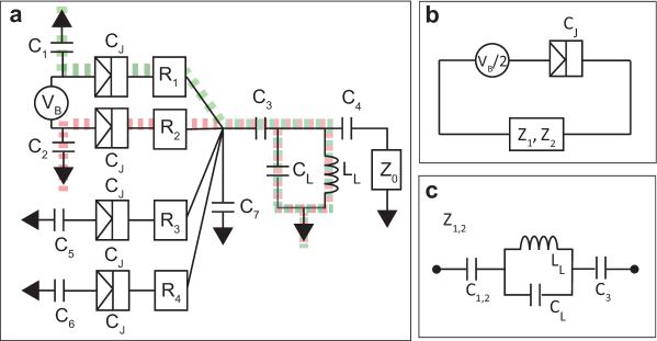
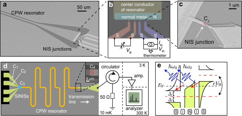
The experimental sample shown in Figure 1a–c consists of NIS tunnel junctions capacitively coupled to a half-wave-length superconducting CPW resonator. Figure 1d depicts the layout of the sample and the measurement setup. Microwave photons, which are generated in the resonator at 10-mK phonon temperature, decay to the transmission line which is capacitively coupled to the resonator, and are characterized using a room temperature spectrum analyzer. To estimate the output power generated by controlled electron tunneling without off-sets, we subtract the output power corresponding to zero bias voltage across the superconductor–insulator–normal-metal–insulator–superconductor (SINIS) junction from the output power at finite bias voltages. As depicted in Figure 1b, a pair of NIS junctions is used to create the photons, while another pair is used as a thermometer to measure the electron temperature of the normal-metal island 36 (see Supporting Information).
To enhance the interaction between the tunneling electrons and the resonator, we use a large coupling capacitance between the normal-metal island and the resonator, , in comparison to the tunnel junction capacitance, . A small enough coupling capacitance between the resonator and the transmission line is employed to maintain a well-defined resonance described by the loaded resonator quality factor . The length of the resonator is chosen to obtain the desired frequency of the output radiation. In this letter, we examine two samples with resonator lengths of mm (Sample A) and mm (Sample B) which correspond to the fundamental resonance frequencies of 4.55 GHz and 8.32 GHz, respectively.
Principle of photon generation
Photon-assisted electron tunneling is the key phenomenon leading to the photon creation in our experiments. When an electron tunnels across an NIS junction, it can absorb energy from or emit energy to the resonator, that is, annihilate or create photons in the resonator 25. Figure 1e illustrates single-electron tunneling events across the NIS junctions and the associated photon creation. When the energy provided by the bias voltage to the electron tunneling across the junction, , is larger than the superconductor gap parameter, , the photon creation rate increases faster as a function of the bias voltage than the annihilation rate. Thus, the effective temperature related to the creation and annihilation of photons increases. The elastic tunneling does not directly affect the resonator modes but dominates the electric current across the junctions for .
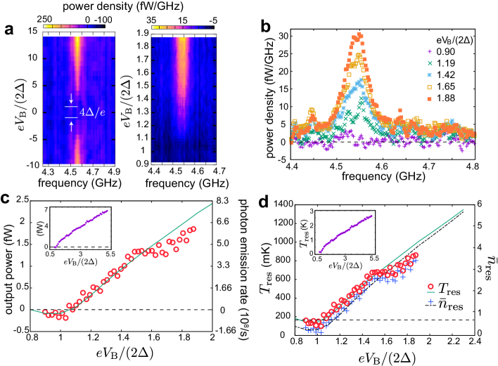
Experiments on Sample A
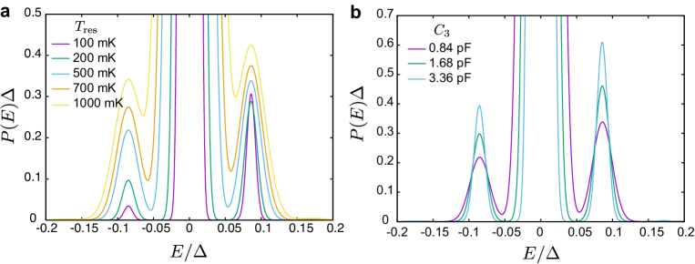
Figure 2a,b shows the output power spectrum of our microwave source as a function of the bias voltage for Sample A. We observe a peak in the output power density around GHz matching the frequency of the fundamental resonator mode estimated using the experimental parameters given in Table 1. The output power density increases with the bias voltage for whereas it is almost vanishing for . This onset of output radiation matching the energy gap in the superconductor density of states provides clear evidence that single-electron tunneling is responsible for the observed photon emission. The bias-voltage dependence of the frequency-integrated output power density, i.e., the net output power is shown in Figure 2c. The onset of positive net power is clearly visible at .
Theoretically, the net output power is related to the average photon numbers of the resonator, , and the transmission line, , at the fundamental angular frequency, , by (see Supporting Information)
| (1) |
where is the characteristic impedance of the transmission line and is the capacitance per unit length of the resonator. In our experiments, the resonator mode is in a thermal state, and hence we may describe its average photon numbers using the Bose distribution function as
| (2) |
With a given , the above equations provide an analytic way of extracting the resonator temperature, , and average photon number directly from the output power.
Although we measure only the difference in the output powers at finite and zero bias voltages, we assume for simplicity that the net output power at zero bias voltage vanishes, i.e., here the resonator is thermalized with the tranmission line. This assumption does not lead to changes in the estimated , but renders to describe the cumulative voltage-bias-independent heating effect of the resonator owing to the transmission line and any additional environments (see Supporting Information). Consequently, we refer below to as the apparent transmission line temperature. Note that the estimated resonator temperature becomes insensitive to changes in at high bias voltages where .
Figure 2d shows the resonator temperature and average photon number corresponding to the measured output power in Figure 2c as functions of the bias voltage. These results indicate that the mode temperature and the average photon number can be efficiently controlled using the bias voltage. For , we have K. Such a high mode temperature is not conveniently achieved by coupling the resonator to a hot resistor due to the transition of the superconducting aluminum, employed as the lead material, to the normal state.
As mentioned above, the electron temperature at the normal-metal island of the NIS junctions is measured using a pair of NIS junctions (see Supporting Information). Importantly, the electron temperature shown in Figure S4b is much lower than that of the resonator mode for almost any bias voltage in Figure 2c,d. This observation verifies that the microwave radiation observed by the spectrum analyzer directly arises from photon-assisted electron tunneling rather than from heating of the normal-metal island.
Although negative net output power is challenging to differentiate in the measured power spectra, we observe in Figure 2c a shallow but statistically significant dip in the experimental output power around . The dip corresponds to the refrigeration of the fundamental mode owing to photon-assisted tunneling, and hence provides complementary evidence of this phenomenon first observed in Ref. 14. In contrast to our measurements of the output radiation, Ref. 14 employs a probe resistor to study the resonator temperature.
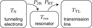
Thermal model
To describe in detail the energy transfer from the tunneling electrons to the transmission line, mediated by microwave photons in the fundamental mode of the resonator, we develop a thermal model shown in Figure 3. Here, we consider thermal states for the electric components assuming that the temperatures of the resonator mode, , and of the electrons in the normal-metal island, , are well defined in the parameter range studied. We have verified the validity of this assumption with a model that accounts for transitions between individual resonator states but do not present the model here since it is unnecessarily complicated. Because of the relatively weak coupling between the resonator and the transmission line, we assume that a tunneling electron does not directly induce photon-assisted transitions in the transmission line. Instead, the influence of the tunneling events is indirectly taken into account through the change in the temperature of the resonator mode.
In the thermal model, the power from the tunneling electrons to the resonator, , is calculated using the theory 25, as detailed in Supporting Information together with the above-discussed power flow from the resonator to the transmission line, . Both of these powers are functions of the temperature of the resonator mode. The output power into the transmission line is calculated by finding the mode temperature, at which these powers balance, . The apparent temperature of the transmission line, corresponding to the photons moving towards the resonator and possible additional heating channels, is assumed to be independent of the applied bias voltage. This is justified for the photons by the employed circulator shown in Figure 1d. The experimentally measured electron temperature of the normal-metal island is used in the simulation.
The theoretical results, employing the parameters given in Table 1, show good agreement with the experiments in a wide range of output powers (see Figure 2c). In the model, the dip in the output power around is fully arising from photon absorption induced by electron tunneling. Furthermore, the modelled average number of photons, , and the temperature of the fundamental mode, are shown in Figure 2d as functions of the bias voltage.
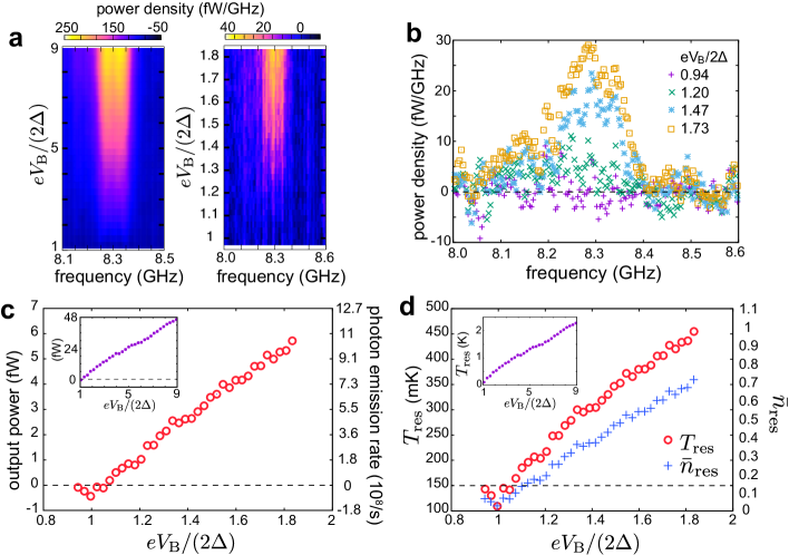
Experiments on Sample B
Experimental results similar to those discussed above are shown in Figure 4 for Sample B. Figure 4a shows the output power density as a function of the frequency and the bias voltage. A peak appears around GHz for and becomes taller with increasing bias voltage. Figure 4b exhibits the traces of the output power density, which are integrated for Figure 4c to obtain the net output power as a function of the bias voltage. The qualitative behavior of the output power matches that of Sample A: the output power begins to increase with bias voltage around , where we observe a shallow dip corresponding to cooling of the resonator. However, the magnitude of the output power is greater and the mode temperature shown in Figure 4d is lower compared with Figure 2. This is because the coupling of the resonator to the transmission line is proportional to the third power of the resonance frequency [see Eq. (1)] which is almost twice as large here in comparison to Sample A.
Discussion
In conclusion, we have measured the spectrum of microwave radiation generated by photon-assisted electron tunneling through NIS junctions. The implemented microwave source realizes direct conversion of the electrostatic energy provided by the dc voltage source to microwave photons. Importantly, it does not rely on the thermal voltage fluctuation spectrum of a resistor, and hence may provide higher effective temperatures, faster tunability, and less excess heating than usual thermal methods. Namely, our results demonstrate the control of the output power up to the regime where the effective mode temperature of the resonator is higher than the critical temperature of the widely used aluminum. The device is compatible with low-temperature electronics and offers in-situ electrical tunability of the output power with the frequency predetermined by the associated resonator. Our measurements of the output power are in good agreement with the corresponding theoretical model, heavily suggesting that our interpretation that photon-assisted tunneling is mainly responsible for the output power is correct. This interpretation is verified by the observation of much higher output powers than what is expected for resonator temperatures matching the normal-metal electron temperature.
Methods
Sample fabrication
The experimental sample shown in Figure 1a–c is fabricated on a high-purity 500-m-thick silicon wafer. The silicon substrate is passivated with a 300-nm-thick thermally grown silicon dioxide. The half-wave-length superconducting CPW resonator is defined with photolithography and reactive ion etching of a 200-nm-thick sputtered Nb layer. Subsequently, a 50-nm-thick layer of Al2O3 is introduced on the whole wafer using atomic layer deposition (ALD) process at 200 ∘C. This ALD oxide serves as the dielectric material of the parallel plate capacitors shown in Figure 1d. The NIS junctions and a transmission line connected to the resonator are subsequently defined using electron beam lithography, followed by a standard two-angle evaporation with in-situ oxidation to form the tunnel barriers. The final NIS nano-structure consists of a 20-nm-thick normal metal (Cu) on top of a 20-nm-thick superconductor (Al), separated by a thin aluminum-oxide tunnel barrier.
Supporting Information
The Supporting Information is available free of charge. Parameters, Apparent transmission line temperature, Energy transfer between tunneling electron and resonator, Energy transfer between resonator and transmission line, Thermometer.
Corresponding Authors
*E-mail: shumpei.masuda@aalto.fi *E-mail: mikko.mottonen@aalto.fi
Author Contributions
Authors S.M. and K.Y.T fabricated the samples and conducted the experiments. S.M. also developed the model and analysed the data. M.P. contributed to the sample fabrication, measurements, and data analysis. R.L. and J.G. contributed to the measurements. M.S and H.G. contributed to the theoretical analysis. M.M. provided the initial ideas and suggestions for the experiment, and supervised the work in all respects. All authors commented on the manuscript written by S.M. and M.M.
Competing Financial Interest
The authors declare no competing financial interest.
We acknowledge the provision of facilities and technical support by Aalto University at OtaNano - Micronova Nanofabrication Centre. We have received funding from the European Research Council under Starting Independent Researcher Grant No. 278117 (SINGLEOUT) and under Consolidator Grant No. 681311 (QUESS), the Academy of Finland through its Centres of Excellence Program (project nos 251748 and 284621) and grants (Nos. 265675, 286215, 276528, 305237, and 305306), the Emil Aaltonen Foundation, the Jenny and Antti Wihuri Foundation, the Alfred Kordelin Foundation, and the Finnish Cultural Foundation. We thank Leif Grönberg for assistance in sample fabrication.
References
- 1 Wolf, E. L. Quantum Nanoelectronics: An Introduction to Electronic Nanotechnology and Quantum Computing (Wiley-VCH, Weinheim, 2009).
- 2 Blais, A., Huang, R. -S., Wallraff, A., Girvin, S. M. & Schoelkopf, R. J. Cavity quantum electrodynamics for superconducting electrical circuits: An architecture for quantum computation. Phys. Rev. A 69, 062320 (2004).
- 3 Wallraff, A., Schuster, D. I., Blais, A., Frunzio, L., Huang, R.-S., Majer, J., Kumar, S., Girvin, S. M. & Schoelkopf, R. J. Strong coupling of a single photon to a superconducting qubit using circuit quantum electrodynamics. Nature 431, 162–167 (2004).
- 4 Majer, J., Chow, J. M., Gambetta, J. M., Koch, J., Johnson, B. R., Schreier, J. A., Frunzio, L., Schuster, D. I., Houck, A. A., Wallraff, A., Blais, A., Devoret, M. H., Girvin, S. M. & Schoelkopf, R. J. Coupling superconducting qubits via a cavity bus. Nature 449, 443–447 (2007).
- 5 Sillanpää, M. A., Park, J. I. & Simmonds, R. W. Coherent quantum state storage and transfer between two phase qubits via a resonant cavity. Nature 449, 438–442 (2007).
- 6 Devoret, M. H. & Schoelkopf, R. J. Superconducting circuits for quantum information: an outlook. Science 339, 1169–1174 (2013).
- 7 Kelly, J. et al. State preservation by repetitive error detection in a superconducting quantum circuit. Nature 519, 66–69 (2015).
- 8 Ofek, N. et al. Extending the lifetime of a quantum bit with error correction in superconducting circuits. Nature 536, 441–445 (2016).
- 9 Inomata, K., Lin, Z. R., Koshino, K., Oliver, W. D., Tsai, J. S., Yamamoto, T. & Nakamura, Y. Single microwave-photon detector using an artificial -type three-level system. Nat. Commun. 7, 12303 (2016).
- 10 Govenius, J., Lake, R. E., Tan, K. Y. & M tt nen, M. Detection of Zeptojoule microwave pulses using electrothermal feedback in proximity-induced Josephson junctions. Phys. Rev. Lett. 117, 030802 (2016).
- 11 Saira, O.-P., Zgirski, M., Viisanen, K. L., Golubev, D. S. & Pekola, J. P. Dispersive thermometry with a Josephson junction coupled to a resonator. Phys. Rev. Applied 6, 024005 (2016).
- 12 Clark, A. M., Miller, N. A., Williams, S., Ruggiero, S. T., Hilton, G. C., Vale, L. R., Beall, K. D., Irwin, K. D. & Ullom, J. N. Cooling of bulk material by electron-tunneling refrigerators. Appl. Phys. Lett. 86, 173508–173510 (2005).
- 13 Timofeev, A. V., Helle, M., Meschke, M., Möttönen, M.& Pekola, J. P. Electronic refrigeration at the quantum limit. Phys. Rev. Lett. 102, 200801 (2009).
- 14 Tan, K. Y., Partanen, M., Lake, R. E., Govenius, J., Masuda, S. & Möttönen, M. Quantum-circuit refrigerator. arXiv:1606.04728 (2016).
- 15 Giazotto, F., Heikkilä, T. T., Luukanen, A., Savin, A. M. & Pekola, J. P. Opportunities for mesoscopics in thermometry and refrigeration: Physics and applications. Rev. Mod. Phys. 78, 217–274 (2006).
- 16 Hofheinz, M., Wang, H., Ansmann, M., Bialczak, R. C., Lucero, E., Neeley, M., O’Connell, A. D., Sank, D., Wenner, J., Martinis, J. M. & Cleland, A. N. Synthesizing arbitrary quantum states in a superconducting resonator. Nature 459, 546–549 (2009).
- 17 Meschke, M., Guichard, W. & Pekola, J. P. Single-mode heat conduction by photons. Nature 444, 187–190 (2006).
- 18 Partanen, M., Tan, K. Y., Govenius, J., Lake, R. E., Mäkelä, K., Tanttu, T. & Möttönen, M. Quantum-limited heat conduction over macroscopic distances. Nat. Phys. 12, 460–464 (2016).
- 19 Houck, A. A., Schuster, D. I., Gambetta, J. M., Schreier, J. A., Johnson, B. R., Chow, J. M., Frunzio, L., Majer, J., Devoret, M. H., Girvin, S. M. & Schoelkopf, R. J. Generating single microwave photons in a circuit. Nature 449, 328–331 (2007).
- 20 Peng, Z. H., de Graaf, S. E., Tsai, J. S. & Astafiev, O. V. Tuneable on-demand single-photon source in the microwave range. Nat. Commun. 449, 12588 (2016).
- 21 Pekola, J. P., Maisi, V. F., Kafanov, S., Chekurov, N., Kemppinen, A., Pashkin, Y. A., Saira, O. -P., Möttönen M. & Tsai, J. S. Environment-assisted tunneling as an origin of the Dynes density of states. Phys. Rev. Lett. 105, 026803 (2010).
- 22 Devoret, M. H., Esteve, D., Grabert, H., Ingold, G.-L.m Pothier, H. & Urbina, C. Effect of the electromagnetic environment on the Coulomb blockade in ultrasmall tunnel junctions. Phys. Rev. Lett. 64, 1824 (1990).
- 23 Girvin, S. M., Glazman, L. I., Jonson, M., Penn, D. R. & Stiles, M. D. Quantum fluctuations and the single-junction Coulomb blockade. Phys. Rev. Lett. 64, 3183 (1990).
- 24 Averin, B., Nazarov, Y. & Odintsov, A. Incoherent tunneling of the cooper pairs and magnetic flux quanta in ultrasmall Josephson junctions. Physica B 165/166, 945–946 (1990).
- 25 Ingold, G. & Nazarov, Y. V. Charge tunneling rates in ultrasmall junctions. NATO ASI Series B 294, 21–107 (1992).
- 26 Zakka-Bajjani, E., Dufouleur, J., Coulombel, N., Roche, P., Glattli, D. C. & Portier, F. Experimental determination of the statistics of photons emitted by a tunnel junction. Phys. Rev. Lett. 104, 206802 (2010).
- 27 Hofheinz, M., Portier, F., Baudouin, Q., Joyez, P., Vion, D., Bertet, P., Roche, P. & Esteve, D. Bright side of the coulomb blockade. Phys. Rev. Lett. 106, 217005 (2011).
- 28 You, J. Q., Liu, Y. X., Sun, C. P. & Nori, F. Persistent single-photon production by tunable on-chip micromaser with a superconducting quantum circuit. Phys. Rev. B 75, 104516 (2007).
- 29 Astafiev, O., Inomata, K., Niskanen, A. O., Yamamoto, T., Pashkin, Y. A., Nakamura, Y. & Tsai, J. S. Single artificial-atom lasing. Nature 449, 588–590 (2007).
- 30 Hauss, J., Fedorov, A., Hutter, C., Shnirman, A. & Schön, G. Single-qubit lasing and cooling at the Rabi frequency. Phys. Rev. Lett. 100, 037003 (2008).
- 31 Grajcar, M., van der Ploeg, S. H. W., Izmalkov, A., Ilichev, H. G. M. E., Fedorov, A., Shnirman, A. & Schön, G. Sisyphus cooling and amplification by a superconducting qubit. Nat. Phys. 4, 612–616 (2008).
- 32 Bruhat, L. E., Viennot, J. J., Dartiailh, M. C., Desjardins, M. M., Kontos, T. & Cottet, A. Cavity photons as a probe for charge relaxation resistance and photon emission in a quantum dot coupled to normal and superconducting continua. Phys. Rev. X 6, 021014 (2016).
- 33 Stockklauser, A., Maisi, V. F., Basset, J., Cujia, K., Reichl, C., Wegscheider, W., Ihn, T., Wallraff, A. & Ensslin, K. Microwave emission from hybridized states in a semiconductor charge qubit. Phys. Rev. Lett. 115, 046802 (2015).
- 34 Childress, L., Sørensen, A. S. & Lukin, M. D. Mesoscopic cavity quantum electrodynamics with quantum dots. Phys. Rev. A 69, 042302 (2004).
- 35 Liu, Y.-Y., Petersson, K. D., Stehlik, J., Taylor, J. M. & Petta, J. R. Photon emission from a cavity-coupled double quantum dot. Phys. Rev. Lett. 113, 036801 (2014).
- 36 Leivo, M. M. & Pekola, J. P. Appl. Phys. Lett. 68, 1996–1998 (1996).
- 37 Gevorgian, S., Linnér, L. J. P. & Kollberg, E. L. CAD models for shielded multilayered CPW. IEEE Trans. Microw. Theory Techn. 43, 772–779 (1995).
- 38 Göppl, M., Fragner, A., Baur, M., Bianchetti, R., Filipp, S., Fink, J. M., Leek, P. J., Puebla, G., Steffen, L. & Wallraff. A. Coplanar waveguide resonators for circuit quantum electrodynamics. J. Appl. Phys. 104, 113904–113911 (2008).
Figures and tables
| SAMPLE A | SAMPLE B | SAMPLE A | SAMPLE B | ||
|---|---|---|---|---|---|
| 13.14 mm | 6.89 mm | 0.84 pF | 0.78 pF | ||
| 220 eV | 191 eV | 0.072 pF | 0.079 pF | ||
| 53 | 52 | ||||
| 159 pF/m | 169 pF/m | 180 mK | 150 mK | ||
| 0.45 H/m | 0.45 H/m | 15.9 dB a | 22 dB b | ||
| 4.55 GHz | 8.32 GHz | 7.8 m | 8.0 m | ||
| 12.5 k | 10.0 k | 5.7 m | 6.1 m | ||
| 3 fF | 3 fF |
a,b The values experimentally measured with a control sample are 13.3 dBa and 19.5 dBb.
1 Supporting information:
Cryogenic microwave source based on nanoscale tunnel junctions
Shumpei Masuda, Kuan Y. Tan, Matti Partanen, Russell E. Lake, Joonas Govenius, Matti Silveri, Hermann Grabert and Mikko Möttönen
1.1 Parameters
The fundamental resonance frequency of a homogeneous half-wavelength CPW resonator of length is given by
| (S1) |
where the speed of light in vacuum is denoted by and the effective relative permittivity of the resonator by . The CPW capacitance and inductance per unit length can be expressed as 37, 38
| (S2) |
where is the complete elliptic integral of the first kind and
| (S3) |
depend on the width of the center conductor , and on the separation between the center conductor and the ground plane of the CPW resonator . We calculate and in Eq. (S2) using Eqs. (S1) and (S3) and the measured values for , , , and given in Table 1. We neglect the kinetic inductance because it is sufficiently smaller than the geometric inductance in Eq. (S2) 38, although in principle, the total inductance per unit length is the sum of the geometric and the kinetic contributions. The resonance frequency calculated using Eq. (S1) and the analytic form of for an unshielded CPW37 has less than 1% difference from the measured value for Sample A and about 4% deviation for Sample B. The characteristic impedance of the transmission line is obtained from .
Capacitances for are estimated using
| (S4) |
where is the area of the parallel-plate capacitor, the permittivity of the aluminum oxide dielectric is denoted by , where is the permittivity of vacuum, and nm is the thickness of the aluminum oxide layer. The capacitance density used for is 75 fF/m2. The tunnel junction area is approximately 200200 nm2 inferred from the SEM image of the sample.
In the absence of an electromagnetic environment, the current through an NIS junction is given by
| (S5) | |||||
where is the electron temperature of the normal-metal island obtained using the thermometer junctions. The superconductor density of states is represented by
| (S6) |
where is the Dynes parameter 15 and is the Fermi–Dirac distribution function
| (S7) |
The tunnel resistance , the Dynes parameter, and the superconductor gap parameter are obtained from a fit of Eq. (S5) to measured junction characteristics.
1.2 Apparent transmission line temperature
In our thermal model in Figure 3, the resonator is thermally connected only to the transmission line and to the tunneling electrons. Due to the simple way the transmission line heats the resonator given by Eq. (1) however, any additional constant heating power to the resonator is accounted in this model by an adjustment of the average photon number of the transmission line. This gives rise to the apparent temperature of the transmission line, , connected to the average photon number, , through the Bose distribution function. Note that is independent of the bias voltage since also the electron temperature of the 50- resistor in Figure 1d giving rise to the photons incident on the resonator does not change with the bias voltage.
Since the power arising from the photon-assisted tunneling is negligible at zero bias voltage, we have in Eq. (1), and hence at zero bias. Thus if we find at any bias voltage, we obtain the temperature and the average photon number of the resonator at zero bias. Consequently, we obtain these quantities at any bias voltage using Eq. (1) and the directly measured power change between the finite and zero bias points.
We use the bias point, at which the measured power change crosses zero, as the calibration voltage for . Here, the net output power given by Eq. (1) and hence the temperature of the resonator coincides with that at zero bias. Thus the power arising from photon-assisted tunneling, , must vanish. As we show in the next section, this calibration point is independent of many of the sample parameters such as the tunnel resistance, . It is also independent of the gain of our amplification chain. Thus our model accurately yields the resonator temperature at the calibration point which equals the apparent transmission line temperature.
1.3 Energy transfer between tunneling electrons and the resonator
The electron tunneling may lead to creation and annihilation of photons at the resonator giving rise to the power transfer in Figure 3. To this end, we employ the theory which has been developed to obtain the electron tunneling rates across tunnel junctions and the resulting energy transfer to the environment 25. In terms of the theory, the environment refers to the electrical degrees of freedom which are coupled to the tunneling process.
The power transfer to the environment strongly depends on the electrical impedance of the system. A simplified electrical circuit diagram of our system is depicted in Figure S1a. The first harmonic mode of the CPW resonator is modeled as a parallel circuit with capacitance , inductance and angular frequency . We assume that the electron tunneling event on either of the junctions is hardly affected by another junction because of a small junction capacitance and large tunneling resistance , and that the direct influence of the transmission line to the electron tunneling is neglected due to a relatively small coupling capacitance . Thus, we consider a pair of separate effective circuits depicted in Figures S1b,c to calculate the tunneling rate at each NIS junction. We assume that the resistance of the normal-metal island is small enough to be neglected because it is in series with the small junction capacitance, and hence negligible current flows through it with respect to Ohmic losses.
The power from the tunneling electrons to the environment is represented by
| (S8) |
where the powers caused by the forward and the backward electron tunneling events at each junction are given by 25
| (S9) | |||||
respectively. Here, and denote the temperatures of the superconductor and of the environment, respectively. The factor of two in Eq. (S8) arises from the fact that the two effective circuits in Figure S1b have an identical contribution to the power. The probability density for the environment to absorb energy during a tunneling event is expressed as 25
| (S10) |
where
| (S11) |
and
| (S12) |
In theory, the effective impedance in Eq. (S11) is the impedance of the external circuit in parallel with . The influence of , which is approximately 3 fF , to the effective impedance is neglected in Eq. (S12) because is dominated by . The influence of is also negligible because it is more than 50 times larger than and approximately cancel out in Eq. (S12).
Note that the environment consists not only of the resonator but also of the capacitors . Finite broadens the peaks of which become delta functions in the limit of infinite . Figure S2a shows of Sample A for various at , where we assumed . The peaks at and correspond to the emission and absorption of a single photon from the resonator, respectively. The high peak at corresponds to the elastic tunnelling. We assume that only the peaks at contribute to . Thus, only a part of contributes to . We compute using Eqs. (S8) and (S9) where we first replace by
| (S13) | |||||
As shown in Figure S2a, the peaks become broader with increasing . The center peak and the side peaks are not well separated for high . Thus, the numerical results of Sample A may have considerable error beyond corresponding to mK [see Figure 2d]. The minor discrepancy between the numerical and experimental results in Figure 2c is attributed to this fact. Figure S2b shows the dependence of on the coupling capacitance . The peak becomes narrower for larger due to the increasing coupling strength between a tunneling electron and the resonator.
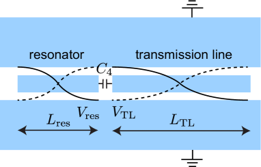
1.4 Energy transfer between the resonator and the transmission line
Let us study a model for the energy transfer between a CPW resonator and a transmission line which are mutually capacitively coupled as shown in Figure S3. First, we model the transmission line as a CPW resonator of finite length and finally extend the length to infinity. The electrostatic energy of the coupling capacitor is given by the voltage difference between the resonator and the transmission line as , where and are the voltage of the resonator and the transmission line at the capacitor, respectively. Thus, the interaction Hamiltonian between the resonator and the transmission line is represented as
| (S14) |
The voltage operators of the resonator and of the transmission line are represented as and , respectively, with the creation operator and the annihilation operator of a photon in the th mode of the resonator and the creation operator and the annihilation operator of a photon in the th mode of the transmission line 2. The coefficients are written as and with the fundamental resonance frequencies . The length of the resonator (transmission line) is (), the capacitance per unit length is () and the inductance per unit length is (). Above, we have assumed that is so small that its effect on and the operators may be neglected.
We employ a basis composed of the energy eigenstates of an uncoupled resonator–transmission-line system. Assuming weak coupling, we may estimate the transition rate from an energy eigenstate to a different one using Fermi’s golden rule, where () denotes the number of photons in the th (th) mode of the resonator (transmission line). The Hamiltonian in Eq. (S14) is rewritten as
| (S15) |
where we omitted the terms proportional to and which do not contribute to the transition rates in Fermi’s golden rule. We first consider the case where a photon in the th mode of the resonator is annihilated and a photon in the th mode of the transmission line is created, i.e., we only consider the term in Eq. (S15). Consequently, the probability that we find the state at time starting from is given by Fermi’s golden rule as
| (S16) | |||||
where with and .
Let us calculate the probability that a photon in the th mode of the resonator is annihilated and a photon in the transmission line is created. To this end, we sum up the probabilities for all photon numbers and every mode in the transmission line. First, we execute the summation over the final photon numbers, which results in
| (S17) |
Next we sum with respect to in the limit where extends to infinity. Thus, we replace the discrete summation over by an integral with respect to energy using the relation
| (S18) |
where . Using Eq. (S18) to sum over in Eq. (S17), the probability of a photon in the th mode to decay given the initial state is represented by
| (S19) | |||||
where and we have introduced a notation and is the photon number in the initial state of the transmission line corresponding to the mode with angular frequency .
Considering all the possible initial states with different photon numbers, the probability of annihilating a photon in the resonator mode , , may be represented as
| (S20) | |||||
where the average photon numbers with angular frequency in the resonator and the transmission line are denoted by and , respectively. Here, is the probability that there are photons with angular frequency in the resonator (transmission line) in the initial state. Hereafter, we replace by for simplicity of notation. Thus, the rate that photons in the resonator with the energy transfer to the transmission line is obtained as
| (S21) |
In the same manner the photon transition rate from the transmission line to the resonator is obtained as
| (S22) |
The total power from the resonator to the transmission line mediated by the photons with angular frequency is represented with the photon numbers in the resonator and the transmission line as
| (S23) | |||||
In the thermal state, we have
| (S24) |
and hence
| (S25) |
owing to Eq. (S23).
1.5 Thermometry
A pair of current-biased NIS junctions is used as a thermometer as illustrated in Figure 1b. The voltage across the thermometer junctions provides a good measure of the electron temperature of the normal-metal island in the temperature range of interest to us. In theory, the tunnel current is written as 25
The current in Eq. (LABEL:eqI1) is approximated by
| (S27) | |||||
where we replaced by because in our case, the current is dominated by the elastic electron tunneling. Here, we neglect the dependence of on justified by . Thus, the voltage essentially depends only on and . For a fixed value of , can be regarded as a single-valued function of . We utilize this property to convert the measured into .
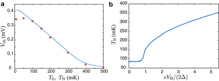
Figure S4a shows the thermometer voltage as a function of the bath temperature measured for 17.7 pA and vanishing bias voltage at the other junctions, . The experimental value of matches the theoretical value obtained from Eq. (S27) for and 100 mK. This is because the electron temperature of the normal-metal island is close to the bath temperature for high . The agreement of the theoretical and numerical results shows that this model of the thermometer is accurate. On the other hand, the experimental values of are lower than the theoretical ones at mK since the electrons thermally decouple from the phonons leading to a saturation of the electron temperature 15. Neverthless, the theoretical model can be used to convert the measured to even in this temperature range and under finite . Figure S4b shows the measured for several bias voltages obtained using the calibration data in Figure S4a.
References
- 1 Wolf, E. L. Quantum Nanoelectronics: An Introduction to Electronic Nanotechnology and Quantum Computing (Wiley-VCH, Weinheim, 2009).
- 2 Blais, A., Huang, R. -S., Wallraff, A., Girvin, S. M. & Schoelkopf, R. J. Cavity quantum electrodynamics for superconducting electrical circuits: An architecture for quantum computation. Phys. Rev. A 69, 062320 (2004).
- 3 Wallraff, A., Schuster, D. I., Blais, A., Frunzio, L., Huang, R.-S., Majer, J., Kumar, S., Girvin, S. M. & Schoelkopf, R. J. Strong coupling of a single photon to a superconducting qubit using circuit quantum electrodynamics. Nature 431, 162–167 (2004).
- 4 Majer, J., Chow, J. M., Gambetta, J. M., Koch, J., Johnson, B. R., Schreier, J. A., Frunzio, L., Schuster, D. I., Houck, A. A., Wallraff, A., Blais, A., Devoret, M. H., Girvin, S. M. & Schoelkopf, R. J. Coupling superconducting qubits via a cavity bus. Nature 449, 443–447 (2007).
- 5 Sillanpää, M. A., Park, J. I. & Simmonds, R. W. Coherent quantum state storage and transfer between two phase qubits via a resonant cavity. Nature 449, 438–442 (2007).
- 6 Devoret, M. H. & Schoelkopf, R. J. Superconducting circuits for quantum information: an outlook. Science 339, 1169–1174 (2013).
- 7 Kelly, J. et al. State preservation by repetitive error detection in a superconducting quantum circuit. Nature 519, 66–69 (2015).
- 8 Ofek, N. et al. Extending the lifetime of a quantum bit with error correction in superconducting circuits. Nature 536, 441–445 (2016).
- 9 Inomata, K., Lin, Z. R., Koshino, K., Oliver, W. D., Tsai, J. S., Yamamoto, T. & Nakamura, Y. Single microwave-photon detector using an artificial -type three-level system. Nat. Commun. 7, 12303 (2016).
- 10 Govenius, J., Lake, R. E., Tan, K. Y. & M tt nen, M. Detection of Zeptojoule microwave pulses using electrothermal feedback in proximity-induced Josephson junctions. Phys. Rev. Lett. 117, 030802 (2016).
- 11 Saira, O.-P., Zgirski, M., Viisanen, K. L., Golubev, D. S. & Pekola, J. P. Dispersive thermometry with a Josephson junction coupled to a resonator. Phys. Rev. Applied 6, 024005 (2016).
- 12 Clark, A. M., Miller, N. A., Williams, S., Ruggiero, S. T., Hilton, G. C., Vale, L. R., Beall, K. D., Irwin, K. D. & Ullom, J. N. Cooling of bulk material by electron-tunneling refrigerators. Appl. Phys. Lett. 86, 173508–173510 (2005).
- 13 Timofeev, A. V., Helle, M., Meschke, M., Möttönen, M.& Pekola, J. P. Electronic refrigeration at the quantum limit. Phys. Rev. Lett. 102, 200801 (2009).
- 14 Tan, K. Y., Partanen, M., Lake, R. E., Govenius, J., Masuda, S. & Möttönen, M. Quantum-circuit refrigerator. arXiv:1606.04728 (2016).
- 15 Giazotto, F., Heikkilä, T. T., Luukanen, A., Savin, A. M. & Pekola, J. P. Opportunities for mesoscopics in thermometry and refrigeration: Physics and applications. Rev. Mod. Phys. 78, 217–274 (2006).
- 16 Hofheinz, M., Wang, H., Ansmann, M., Bialczak, R. C., Lucero, E., Neeley, M., O’Connell, A. D., Sank, D., Wenner, J., Martinis, J. M. & Cleland, A. N. Synthesizing arbitrary quantum states in a superconducting resonator. Nature 459, 546–549 (2009).
- 17 Meschke, M., Guichard, W. & Pekola, J. P. Single-mode heat conduction by photons. Nature 444, 187–190 (2006).
- 18 Partanen, M., Tan, K. Y., Govenius, J., Lake, R. E., Mäkelä, K., Tanttu, T. & Möttönen, M. Quantum-limited heat conduction over macroscopic distances. Nat. Phys. 12, 460–464 (2016).
- 19 Houck, A. A., Schuster, D. I., Gambetta, J. M., Schreier, J. A., Johnson, B. R., Chow, J. M., Frunzio, L., Majer, J., Devoret, M. H., Girvin, S. M. & Schoelkopf, R. J. Generating single microwave photons in a circuit. Nature 449, 328–331 (2007).
- 20 Peng, Z. H., de Graaf, S. E., Tsai, J. S. & Astafiev, O. V. Tuneable on-demand single-photon source in the microwave range. Nat. Commun. 449, 12588 (2016).
- 21 Pekola, J. P., Maisi, V. F., Kafanov, S., Chekurov, N., Kemppinen, A., Pashkin, Y. A., Saira, O. -P., Möttönen M. & Tsai, J. S. Environment-assisted tunneling as an origin of the Dynes density of states. Phys. Rev. Lett. 105, 026803 (2010).
- 22 Devoret, M. H., Esteve, D., Grabert, H., Ingold, G.-L.m Pothier, H. & Urbina, C. Effect of the electromagnetic environment on the Coulomb blockade in ultrasmall tunnel junctions. Phys. Rev. Lett. 64, 1824 (1990).
- 23 Girvin, S. M., Glazman, L. I., Jonson, M., Penn, D. R. & Stiles, M. D. Quantum fluctuations and the single-junction Coulomb blockade. Phys. Rev. Lett. 64, 3183 (1990).
- 24 Averin, B., Nazarov, Y. & Odintsov, A. Incoherent tunneling of the cooper pairs and magnetic flux quanta in ultrasmall Josephson junctions. Physica B 165/166, 945–946 (1990).
- 25 Ingold, G. & Nazarov, Y. V. Charge tunneling rates in ultrasmall junctions. NATO ASI Series B 294, 21–107 (1992).
- 26 Zakka-Bajjani, E., Dufouleur, J., Coulombel, N., Roche, P., Glattli, D. C. & Portier, F. Experimental determination of the statistics of photons emitted by a tunnel junction. Phys. Rev. Lett. 104, 206802 (2010).
- 27 Hofheinz, M., Portier, F., Baudouin, Q., Joyez, P., Vion, D., Bertet, P., Roche, P. & Esteve, D. Bright side of the coulomb blockade. Phys. Rev. Lett. 106, 217005 (2011).
- 28 You, J. Q., Liu, Y. X., Sun, C. P. & Nori, F. Persistent single-photon production by tunable on-chip micromaser with a superconducting quantum circuit. Phys. Rev. B 75, 104516 (2007).
- 29 Astafiev, O., Inomata, K., Niskanen, A. O., Yamamoto, T., Pashkin, Y. A., Nakamura, Y. & Tsai, J. S. Single artificial-atom lasing. Nature 449, 588–590 (2007).
- 30 Hauss, J., Fedorov, A., Hutter, C., Shnirman, A. & Schön, G. Single-qubit lasing and cooling at the Rabi frequency. Phys. Rev. Lett. 100, 037003 (2008).
- 31 Grajcar, M., van der Ploeg, S. H. W., Izmalkov, A., Ilichev, H. G. M. E., Fedorov, A., Shnirman, A. & Schön, G. Sisyphus cooling and amplification by a superconducting qubit. Nat. Phys. 4, 612–616 (2008).
- 32 Bruhat, L. E., Viennot, J. J., Dartiailh, M. C., Desjardins, M. M., Kontos, T. & Cottet, A. Cavity photons as a probe for charge relaxation resistance and photon emission in a quantum dot coupled to normal and superconducting continua. Phys. Rev. X 6, 021014 (2016).
- 33 Stockklauser, A., Maisi, V. F., Basset, J., Cujia, K., Reichl, C., Wegscheider, W., Ihn, T., Wallraff, A. & Ensslin, K. Microwave emission from hybridized states in a semiconductor charge qubit. Phys. Rev. Lett. 115, 046802 (2015).
- 34 Childress, L., Sørensen, A. S. & Lukin, M. D. Mesoscopic cavity quantum electrodynamics with quantum dots. Phys. Rev. A 69, 042302 (2004).
- 35 Liu, Y.-Y., Petersson, K. D., Stehlik, J., Taylor, J. M. & Petta, J. R. Photon emission from a cavity-coupled double quantum dot. Phys. Rev. Lett. 113, 036801 (2014).
- 36 Leivo, M. M. & Pekola, J. P. Appl. Phys. Lett. 68, 1996–1998 (1996).
- 37 Gevorgian, S., Linnér, L. J. P. & Kollberg, E. L. CAD models for shielded multilayered CPW. IEEE Trans. Microw. Theory Techn. 43, 772–779 (1995).
- 38 Göppl, M., Fragner, A., Baur, M., Bianchetti, R., Filipp, S., Fink, J. M., Leek, P. J., Puebla, G., Steffen, L. & Wallraff. A. Coplanar waveguide resonators for circuit quantum electrodynamics. J. Appl. Phys. 104, 113904–113911 (2008).