Propagating Polaritons in III-Nitride Slab Waveguides
Abstract
We report on III-nitride waveguides with c-plane GaN/AlGaN quantum wells in the strong light-matter coupling regime supporting propagating polaritons. They feature a normal mode splitting as large as 60 meV at low temperatures thanks to the large overlap between the optical mode and the active region, a polariton decay length up to 100 m for photon-like polaritons and lifetime of 1-2 ps; with the latter values being essentially limited by residual absorption occurring in the waveguide. The fully lattice-matched nature of the structure allows for very low disorder and high in-plane homogeneity; an important asset for the realization of polaritonic integrated circuits that could support nonlinear polariton wavepackets up to room temperature thanks to the large exciton binding energy of 40 meV.
pacs:
I Introduction
Over the past 15 years, optical interconnects, which are essential building blocks for the realization of photonic platforms fully-integrated on a chip – so-called photonic integrated circuits (PICs), have triggered a huge interest due to their promising potential in the field of information technology for the realization of small-footprint low-energy devices that may also offer a high clock rate and eventually support strong nonlinearity.Miller (2009)
Among the various systems at play, one such interesting platform deals with exciton-polaritons, hereafter called polaritons, in the waveguide geometry. Polaritons are quasiparticles that arise from the hybridization between a (confined) photon mode and a semiconductor exciton in the so-called strong coupling regime (SCR).Weisbuch et al. (1992) Their properties are therefore intermediate between those of photons and excitons and as such they benefit from the best of both worlds. Polaritons can propagate at near light speed and interact through their exciton fraction. This makes them ideal candidates for low-power active all-optical devices such as switches, optical transistors and logic gates.Liew et al. (2008); Amo et al. (2010) One of the inherent difficulties with all-optical devices is the lack of interaction between photons, which makes it nearly impossible to directly modify a light beam with a second one. To operate a nonlinear all-optical device made from traditional dielectric materials very high intensities are required, with typical values for the nonlinear refractive index on the order of cm2/W,Boyd (2008) and present plasmonic alternatives are inherently lossy. Wurtz and Zayats (2008) A polariton-based device, however, combines a strong nonlinearity — on the order of 10-10 cm2/W — with a very fast response time on the order of a few picoseconds.Amo et al. (2010); Walker et al. (2015)
In order to reach the SCR between excitons and photons, and maximize the normal mode splitting between polariton eigenmodes, it is paramount to reduce any source of decoherence and maximize the exciton-photon coupling strength . For a confined optical mode coupled to quantum well (QW) excitons, it can be expressed as Savona et al. (1995); Fox (2006)
| (1) |
where is the reduced Planck constant, is the elementary charge, is the effective number of QWs (i.e. the nominal number of QWs weighted by the intensity of the optical mode profile) that are coupled to the optical mode, is the oscillator strength per unit area of the QW exciton, is the free electron mass, is the permittivity of vacuum, is the effective refractive index of the optical mode and is the corresponding modal effective length.sup From this equation, we can see the interest in using QWs supporting large oscillator strength excitons and promoting structures with a large . In addition, in order to maintain the SCR up to room temperature or above, the QW excitons should be stable at these elevated temperatures. This requirement favors direct wide bandgap semiconductors which naturally have large exciton binding energies.
As previously mentioned, the waveguide geometry is a promising platform for strong coupling applications.Ellenbogen and Crozier (2011); Takeda and Sakoda (2012); Walker et al. (2013); Solnyshkov et al. (2014); Rosenberg et al. (2016) Indeed, the high in-plane group velocity on the order of m/s in waveguides makes them attractive for the achievement of fast PICs. Optical confinement provided by total internal reflection (TIR) results in smaller optical leakage and a small value compared to distributed Bragg reflector (DBR) confinement traditionally used in planar microcavities (MCs). This is particularly the case for III-nitrides as the refractive index contrast between materials is low. The present III-nitride waveguide —as detailed below— supports a mode with an effective length of 175 nm, whereas a comparable III-nitride MC has an effective length of 590 nm.Christmann et al. (2008a) A waveguide is also more robust against any deviations in layer thickness compared to MCs, since a guided mode does not depend on the cladding thickness and only slightly on the core dimensions, hence leading to higher fabrication yields. Additionally, the waveguide geometry can allow for easy potential landscaping by electrical gating Rosenberg et al. (2016) and electrical injection of carriers – as is commonly done in edge-emitting laser diodes (LDs) – as opposed to electrical injection through DBRs, which is a much more challenging task. As an illustration of the potential of strongly coupled waveguides, let us note that nonlinear effects relying on the formation of dark-bright spatio-temporal polariton soliton wavepackets with energies as low as 0.5 pJ has been recently reported in GaAs-based structures operating at 10 K.Walker et al. (2015)
In this work, we report on a III-nitride slab supporting waveguided polaritons originating from the hybridization of GaN/AlGaN multiple QW (MQW) excitons with the propagating TE0 optical mode. Waveguided polaritons are monitored up to 100 K with a normal mode splitting of 60 meV. The guided polaritons propagate with a decay length of about 100 m and have a lifetime of 1-2 ps. The sample structure is first discussed in Section II. The properties of the bare QW excitons and guided polaritons are then analyzed in Sections III and IV, respectively. The main conclusions and an outlook toward future work are given in Section V.
II Sample Structure
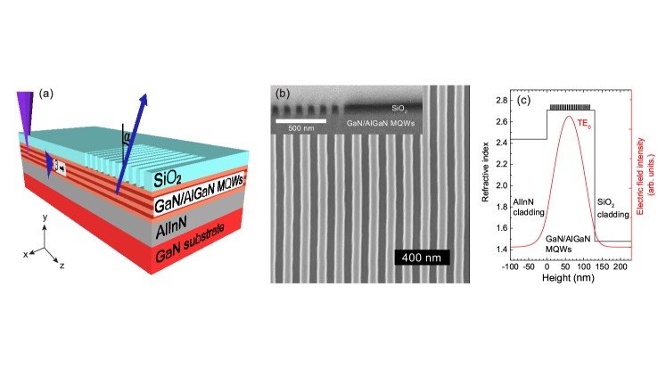
The structure under investigation is sketched in Fig. 1(a) and consists of a 130 nm thick active region with 22 GaN/Al0.1Ga0.9N (1.5 nm/3.5 nm) QWs sandwiched between a 400 nm thick Al0.83In0.17N bottom cladding lattice-matched to GaN and a 100 nm thick SiO2 top cladding. The bottom cladding and the active region were grown by metalorganic vapor phase epitaxy in an AIXTRON 200/4 RF-S reactor on a low dislocation density ( cm-2) freestanding (FS) c-plane GaN substrate. High-quality AlInN layers have been demonstrated on these substratesCosendey et al. (2011); Perillat-Merceroz et al. (2013) and have been successfully used for optical mode confinement in the waveguide region of visible III-nitride edge-emitting LDs.Castiglia et al. (2010) The AlInN bottom cladding layer contains seven 5 nm thick GaN interlayers positioned 50 nm apart in order to avoid kinetic roughening of the AlInN alloy. Perillat-Merceroz et al. (2013) Note that the effect of the quantum confined Stark effect (QCSE) on the exciton oscillator strength is negligible due to the reduced thickness (1.5 nm) of the present GaN/AlGaN QWs and the low Al content in the barriers.Grandjean et al. (1999) This is confirmed by the elevated value of 0.8 for the electron-hole overlap integral for these QWs, as calculated with the formalism (see Section III for further details). In addition, the use of an AlGaN barrier width of 3.5 nm avoids any coupling between adjacent wells. All aforementioned layer thicknesses are measured by high-resolution X-ray diffraction (HR-XRD). sup
A significant advantage of the polariton waveguide geometry over the more conventional planar MC design employing similar GaN/AlGaN QWs is that the bottom cladding can be grown lattice-matched to the FS-GaN substrate. Indeed in the MC case, a substantial Al concentration is required in the two quarterwave layers of the bottom UV DBR to avoid unwanted absorption at the GaN QW energy.Christmann et al. (2008a) The resulting lattice-mismatch between the GaN template and the UV AlInN/AlGaN DBR requires the implementation of specific strain engineering solutions to avoid the formation of cracksFeltin et al. (2006) and leads to a higher density of defects, mainly threading dislocations, as there would be no additional benefit in using FS-GaN substrates in this latter case. The entire present structure is pseudomorphic to the FS-GaN substrate, as confirmed by HR-XRD reciprocal space mapping.sup
The SiO2 top cladding was deposited by plasma-enhanced chemical vapor deposition on top of the active region. In order to outcouple the guided modes from the waveguide for subsequent analyses, a grating coupler was defined in the top claddingTaillaert et al. (2006) by electron beam lithography using a 100 keV Vistec EBPG5000 e-beam lithography system and ZEP520A positive resist, and inductively coupled plasma etching with CHF3/SF6 chemistry. A scanning electron micrograph (SEM) of the fabricated structure in top view and cross-section is shown in Fig. 1(b). The etched sidewalls form an angle of 3∘° with the vertical. The aspect ratio of the etched slits is 5:3. The gratings have a period of 125 nm with 50% fill factor and span over a 100 100 m2 area.
We can relate the propagation constant of the guided mode to the emission angle (shown in Fig. 1(a)) from the grating output coupler by the relation
| (2) |
where is the diffraction order. We use a first-order grating to maximize the outcoupled light intensity. The grating period is chosen such that the central in-plane wavevector of interest (50 m-1) is emitted perpendicular to the sample.
A slab waveguide can support both transverse electric (TE, with the electric field along x) and transverse magnetic (TM, with the magnetic field along x and the electric field in the yz-plane) guided modes. We define z as the propagation direction of the guided modes, y the growth direction of the sample and x the direction perpendicular to both of these, as shown in Fig. 1(a). The thickness of the waveguide core was chosen such that only the TE0 and TM0 modes are supported and all higher order modes are cut off. This prevents the excitons from coupling to multiple modes, which would act as a lossy channel for the photogenerated carriers. The XA exciton couples exclusively, as XB mostly does, to the in-plane electric field as deduced from calculations, which favors the TE mode over the TM one. The overlap integral of the field of the TM0 mode with the active region is almost two orders of magnitude smaller than the overlap integral of the TE0 field with the active region. Therefore, we will only consider the TE0 mode in the remaining part of this work.
The present structure was optimized to maximize the light-matter coupling strength between the guided photons and MQW excitons. The high number of QWs (22) combined with the large overlap between the optical mode and the QWs – the TE0 mode has no nodes and the mode intensity quickly decreases outside the active region, as can be seen in Fig. 1(c) – and the large oscillator strength of the QWs result in a high value of 30 meV.
III Bare Quantum Well Properties
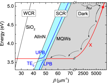
In the present structure, three different light-matter coupling regimes can potentially coexist in distinct zones of the energy vs. diagram as shown in Fig. 2. Photons with an in-plane wavevector outside the active region light cone do not exist; hence explaining the terminology dark excitons as the radiative recombination of excitons in this region is forbidden. In the -space region between the bottom cladding and the active region light cone, photons are tightly confined in the waveguide by TIR and, as will be shown in Section IV, they hybridize with the XA excitons. Inside the bottom cladding light cone, TIR is lost at the bottom interface and the active region becomes a lossy resonator with broad optical modes. Therefore excitons and photons are weakly coupled in this region. Inside the top cladding light cone, TIR is also suppressed at the top interface and the structure forms a low quality factor () Fabry-Perot resonator. As a result, we simultaneously have three populations of excitations in the sample under cw non-resonant excitation: dark excitons, waveguided polaritons, and weakly coupled excitons. The latter population allows us to probe the bare excitonic properties inside the air light cone using conventional optical spectroscopy techniques.
We calculated the confined MQW electron and hole energy levels at 0 K using the formalismsup ; Chuang and Chang (1996) adapted for the analysis of strained MQW structures. Due to the geometrical effect in the MQW, the value of the electric field found by setting the potential difference between the extremities of the active region to zero, amounts to 220 kV/cm in the AlGaN barriers and -625 kV/cm in the GaN wells, respectively.Bernardini and Fiorentini (1999) An excitonic energy 3.566 eV and 3.576 eV is obtained for XA for XB, respectively, assuming an exciton binding energy of 40 meV in both cases. The latter was deduced from the variational approach developed by Leavitt and Little.Leavitt and Little (1990) The relative oscillator strength of the XA (0.5 for light polarized along both and , 0 along ) and XB excitons (0.495 for light polarized along both and , 0.01 along ) shows an exclusive coupling for XA and a heavily preferential coupling for XB to the in-plane electric field. Hence it explains the poor excitonic coupling to the TM modes supported by the waveguide.
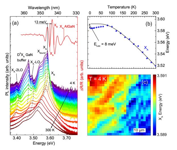
The bare exciton properties were experimentally investigated by photoreflectance (PR) and micro-photoluminescence (-PL) spectroscopy.sup Clear signatures can be observed in the low temperature PR spectrum (shown in Fig. 3(a)) for the XA and XB QW excitons as well as the XA barrier exciton. No signature of the underlying FS-GaN substrate was observed in PR as with this technique the modulation induced by photogenerated carriers essentially occurs in the topmost layers. The critical points were fitted using the approach introduced by Aspnes.Aspnes (1973); Glauser et al. (2014) The comparison between low-temperature PL and PR spectra (Fig. 3(a)) reveals a Stokes shift of meV, which is similar to that previously reported for equivalent GaN/AlGaN MQW samples.Glauser et al. (2014) Note that since the PL and PR measurements were conducted with the sample in different cryostats, there is an uncertainty of 500 m —comparable to the PR spot size— on the relative sample location probed in both experiments. On the low-temperature PL spectra, we can clearly identify the XA MQW exciton together with its first and second longitudinal optic (LO) phonon replicas, each separated by 92 meV, the accepted LO-phonon energy for GaN. An inhomogeneous broadening of 8 meV is measured at 4 K for the XA peak. This very low value for a sample that consists of 22 QWs indicates the high quality of the latter, which compares favorably with state-of-the-art GaN/AlGaN QW samples.Feltin et al. (2007); Stokker-Cheregi et al. (2008); Glauser et al. (2014) On the low-energy side of the XA exciton, we observe a shoulder which is likely due to a bound excitonic states, Xbound. It could originate from the incorporation of acceptor-like impurities such as carbon during the low-temperature growth of the MQWs.Cingolani et al. (1997); Weisbuch (2016) At low temperatures, a third peak is present at 3.55 eV. This energy corresponds to the maximum of the polariton emission —see below— and as such, this peak could be the signature of scattered lower polaritons.
The temperature dependence of the XA transition can be well described by the expression:Viña et al. (1984)
| (3) |
where is the expected energy of the free exciton transition at 0 K and the second term is the Bose-Einstein occupation factor for phonons where is an electron-phonon coupling constant and is an average phonon temperature. This model is notably more accurate than Varshni’s empirical law at low temperature.Brunner et al. (1997) Upon fitting the measured PL emission energies to Eq. 3 (Fig. 3(b)), we find a localization energy of 8 meV, together with values of 70 meV and 322 K for and , respectively. These values for the latter two parameters are in good agreement with those reported by Brunner et al. for bulk (Al)GaN layers.Brunner et al. (1997)
The energy of the XA free exciton deduced fom PR measurements (3.599 eV at 10 K) and Eq. 3 (3.592 eV at 4 K) is slightly higher than that originally expected from calculations (3.566 eV). This could be accounted for assuming a smaller value of the built-in electric field in the MQWs and slightly different in-plane carrier masses.
The in-plane homogeneity of the sample was checked through -PL mapping performed at 4 K (Fig. 3(c)), which leads to a standard deviation as low as 0.42 meV for the XA energy over a 50 50 m2 area. This shows the high degree of homogeneity of the sample, which is an important asset for the control of waveguided polaritons and the potential realization of PICs relying on such an approach. The uniformity of those waveguide samples can likely be ascribed to the growth performed on low defect density FS-GaN substrate, as these latter samples are expected to be much less affected by in-plane disorder than their strongly coupled counterparts grown on c-plane sapphire substrate. Feltin et al. (2007); Rossbach et al. (2013)
To summarize this section, the low values of the inhomogeneous PL broadening (8 meV), localization energy (8 meV), Stokes shift (13 meV) and in-plane inhomogeneity ( = 0.42 meV) highlight the high quality and the homogeneity of the present sample, especially when taking into account the large number of QWs.
IV Guided Polaritons
The waveguide dispersion curve was measured for various propagation distances by moving the excitation spot away from the grating outcoupler between 4 and 100 K. The measured signal intensity is relatively weak for two reasons. First, only excitons lying outside the cladding light cone are expected to form polaritons, as shown in Fig. 2, hence the excitonic fraction that relaxes into this light cone does not contribute to the signal. Second, as the slab waveguide is radially symmetric, waveguided polaritons, if present, will propagate isotropically from the excitation spot. Therefore, only polaritons within the angle covered by the collection zone can contribute to the signal and its intensity will approximately decrease as the reciprocal of the propagation distance . This approximation holds well if the size of the collection region is substantially smaller than the propagation distance. Here, the collection region is 19 m and the propagation distances used in the experiments range between 30 and 200 m. Additionally, the internal quantum efficiency of the active medium decreases with increasing temperature, which further reduces the signal intensity at higher temperatures. Above 100 K, the signal intensity became too weak to perform any reliable measurements. Note however, that this does not imply that the SCR could not be maintained above 100 K.
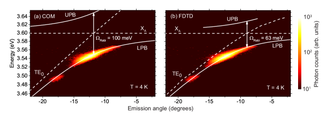
An example of a dispersion curve measured at = 4 K is shown in Fig. 4 where the background signal coming from bare excitons was removed for clarity.sup We clearly see a pronounced curvature in the measured signal, which is ascribed to the avoided crossing of lower polaritons with the uncoupled free XA transition.XBn We compared the measured signal at 4 K to both a simple coupled oscillator model (COM) and full two-dimensional finite-difference time-domain (2D-FDTD) calculations.sup The COM uses a constant value of , and therefore a linear dispersion for the uncoupled TE0 waveguide mode. By fitting this model (the results are shown in Fig. 4(a)), we find a normal mode splitting of 100 meV for this measurement. Application of Eq. 1 results in an oscillator strength of cm-2 for the QW excitons. The 2D-FDTD calculations on the other hand take the material refractive index dispersion into account. The resulting uncoupled TE0 mode is curved due to the increase in refractive index of the QWs and barriers near the band edge, located at 3.64 and 3.71 eV, respectively, as shown in Fig. 4(b). The 2D-FDTD calculations were performed for various values of , and a good fit to the data was found for cm-2. The corresponding normal mode splitting is 63 meV. The discrepancy in the values of and between the COM and the 2D-FDTD calculations is mainly due to the neglected refractive index dispersion in the former case. Since the uncoupled mode is bent in the same direction as the anticrossing by the increasing refractive index toward the band edge, a smaller oscillator strength is required to reproduce the measured dispersion. A COM featuring a constant effective refractive index therefore systematically overestimates the exciton oscillator strength and the normal mode splitting. This comparison shows the importance of the effect of the refractive index dispersion in the analysis of photonic structures operating near the band edge. Note that a value of cm-2 was previously reported for similar QWs embedded in a strongly coupled MC using transfer matrix simulations accounting for dispersion.Glauser et al. (2014) Let us point out that the observed curvature in the dispersion cannot be explained by the increase in the refractive index of the active region near the band gap as can be seen in Fig. 4(b), which confirms that the present structure is operating in the SCR.
We do not observe the highly excitonic tail of the LPB, since the polaritons relax to lower energy states and because the outcoupling rate is proportional to their photon fraction. The photonic tail of the LPB is hardly visible in the measured polariton dispersions, most likely due to the relaxation bottleneck of highly photonic polaritons.Tassone et al. (1997) Note that there is a second maximum in the polariton emission intensity at 92 meV below the localized XA emission energy. This could be explained by the LO-phonon assisted relaxation of excitons to the LPB as already reported in the planar MC case.Corfdir et al. (2012)
By comparison with 2D-FDTD calculations, we find a normal mode splitting of 63 meV for the curve measured at 4 K (Fig. 4(b)), and an average splitting of 60 meV between 4 and 100 K. Such a value has to be compared to the 56-60 meV reported by Christmann et al. for a III-nitride planar MC containing 67 GaN/AlGaN QWs.Christmann et al. (2008b) The similar value of recorded for the two geometries is the direct manifestation of the increased value in waveguide structures.
The absence of the UPB in the PL spectra is a well-known feature of wide band gap systems,Christmann et al. (2008a); Guillet et al. (2011) which is mainly due to absorption occurring above the MQW band gap and the large value, which hinders the thermal promotion of polaritons to the UPB.Tassone et al. (1997) However, let us note that even in GaAs-based polariton waveguides, the UPB luminescence is usually rather weak or even absent.Walker et al. (2013); Tinkler (2015); Rosenberg et al. (2016)
We did not observe any renormalization effects, i.e., any decrease in the normal mode splitting, with increasing pumping power up to 6 kW/cm2. This is because we cannot measure any dispersion relation for propagation distances shorter than 20 m. For these short distances, the outcoupled guided light is not distinguishable from the very intense direct PL signal originating from the MQWs inside the air light cone. Therefore, we essentially probed regions where the reduction in the polariton density coming from their radial outspread is significant and renormalization should not be expected.Rossbach et al. (2013); Sturm et al. (2014)
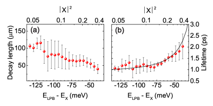
In addition to the above-mentioned temperature dependence, the observed decrease in the signal intensity with increasing propagation distance is not only due to the radial spread-out of waveguided polaritons from the excitation spot – which leads to a decrease in the polariton density overlapping with the collection area as – but also to polaritonic decay. Indeed, as waveguided polaritons propagate, they experience an intrinsic decay following an exponential Beer-Lambert law, mainly due to photonic losses for the present exciton-photon detunings (). In order to determine their intrinsic decay length – defined as the distance over which the integrated polariton PL intensity at the excitation spot is reduced by a factor – and hence their lifetime, the measured integrated PL intensity is multiplied by the propagation distance which is fitted to an exponential decay. The obtained decay length as a function of polariton energy is shown in Fig. 5(a). Polaritons with a large photonic fraction in excess of 0.94 are characterized by a decay length larger than 100 m, which decreases as the excitonic fraction becomes larger. To further support this analysis, the absorption coefficient in the waveguide was determined by the variable stripe length method to be 60 cm-1 at around 200 meV below the free XA energy,sup which corresponds to a decay length of 167 m. This puts an upper limit to the propagation length of photons and highly photonic polaritons in the present sample and is mainly limited by residual absorption from the QWs. We can expect the absorption to be higher —and the corresponding decay length lower— for higher energies. Since the value of 167 m only slightly exceeds the measured polariton decay lengths at energies between 120 and 140 meV below XA, absorption is most likely the limiting factor of polariton propagation.
Another essential figure of merit to qualify the present structure is the polariton lifetime . The latter is given by
| (4) |
where and are the photon and exciton lifetime, respectively, and are the usual Hopfield coefficients and and give the photon and exciton fraction of the polaritons, respectively.Hopfield (1958) The polariton lifetime was determined by dividing the measured polariton decay length by the group velocity of the LPB, defined as , (Fig. 5(b)). Values ranging between 1 and 2 ps were derived for polaritons with an exciton fraction between 0.05 and 0.4. The free XA lifetime was determined by time-resolved PL to be 325 ps at K. A fit from Eq. 4 to the data leads to a value of 0.9 ps for , which corresponds to a photonic linewidth meV and an optical quality factor of . This photonic lifetime is about a factor of 5 larger than that reported for comparable III-nitride planar MCs,Levrat et al. (2010) essentially due to the improved confinement provided by TIR. Note that we do not directly observe the photonic and excitonic linewidths stated above in the measured dispersion signal for highly photonic and excitonic polaritons, respectively. In addition to this broadening along the energy axis, there is indeed an extra source of broadening in the emission angle due to fabrication inhomogeneities in the grating coupler. For highly photonic polaritons, the energy linewidth becomes relatively small and the observed signal broadening is of purely angular origin. In this limit, we observe an angular full width at half maximum linewidth (FWHM) of 1.2∘, which corresponds to a FWHM wavevector linewidth of 0.34 m-1 and a FWHM error on the grating period nm through Eq. 2. The normal mode splitting of 60 meV corresponds to a Rabi period, i.e., the period of the coherent oscillations between the photon and exciton fraction of the polariton, as short as 69 fs. In this respect, we point out that the present sample is characterized by a large polariton lifetime to Rabi period ratio. When comparing the present values to those obtained in GaAs-based waveguides,Walker et al. (2013) the shorter decay lengths and lifetimes in III-nitride structures are likely due to the combination of an enhanced sensitivity to photonic disorder of short wavelength systems together with the increased QW absorption below the band gap and the high number of QWs. If we compare the obtained values for the decay length to the ballistic condensate propagation on the order of 10 m reported by Hahe et al. in a ZnO planar MC,Hahe et al. (2015) the much larger decay length in the present case can be well accounted for by TIR confinement and the larger polariton propagation velocity.
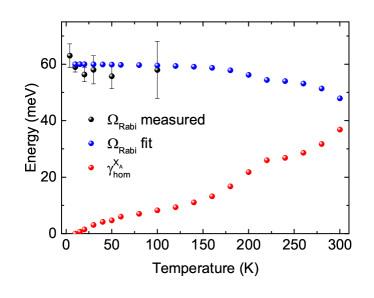
Additional information on the temperature dependence of the SCR can be obtained by considering the relation
| (5) |
which is derived from the COM.sup We assume the photonic linewidth to be temperature-independent. The homogeneous excitonic linewidth of the XA exciton, , was extracted by fitting a Voigt peak profile to the temperature-dependent PL data shown in Fig. 3(a). Note that we only take the homogeneous broadening into account, since the normal mode splitting does not depend on the inhomogeneous broadening when the normal mode splitting to MQW inhomogeneous broadening ratio is large.Houdré et al. (1996); Christmann et al. (2006) The calculated values of are shown in Fig. 6, together with . Based on these calculations, we can predict a slight decrease in the normal mode splitting down to 48 meV at 300 K. This again confirms the strong potential of the present platform to investigate the SCR up to room temperature.
V Conclusion and Outlook
In conclusion, we demonstrated propagating polaritons in III-nitride slab waveguides, where c-plane GaN/AlGaN MQW excitons hybridize with the propagating TE0 optical mode. The fully lattice-matched growth leads to a very low disorder and high in-plane homogeneity. The SCR was observed up to 100 K with an average normal mode splitting as high as 60 meV due to the large overlap between the QWs and the waveguide mode. The guided polaritons feature a decay length of 50 to 100 m and a lifetime of 1-2 ps, which are well accounted for by residual absorption in the QWs.
Such a structure shows great potential for photonic and polaritonic integrated circuits up to room temperature. In this perspective, ridge waveguides with lateral confinement would prove a more practical geometry for devices, as it would prevent the isotropic propagation of polaritons. Consequently, the signature of waveguided polaritons should be measurable over longer distances and up to higher temperatures. It would also open the possibility to explore polariton nonlinearities, e.g. polariton soliton wavepackets up to room temperature.
Acknowledgements.
We would like to thank the Swiss National Science Foundation for financial support through Grant No. 200020_162657.References
- Miller (2009) D. A. B. Miller, “Device requirements for optical interconnects to silicon chips,” Proc. IEEE 97, 1166–1185 (2009).
- Weisbuch et al. (1992) C. Weisbuch, M. Nishioka, A. Ishikawa, and Y. Arakawa, “Observation of the coupled exciton-photon mode splitting in a semiconductor quantum microcavity,” Phys. Rev. Lett. 69, 3314–3317 (1992).
- Liew et al. (2008) T. C. H. Liew, A. V. Kavokin, and I. A. Shelykh, “Optical circuits based on polariton neurons in semiconductor microcavities,” Phys. Rev. Lett. 101, 016402 (2008).
- Amo et al. (2010) A. Amo, T. C. H. Liew, C. Adrados, R. Houdré, E. Giacobino, A. V. Kavokin, and A. Bramati, “Exciton-polariton spin switches,” Nat. Photon. 4, 361 (2010).
- Boyd (2008) R.W. Boyd, Nonlinear Optics, Nonlinear Optics Series (Academic Press, Cambridge, 2008).
- Wurtz and Zayats (2008) G. A. Wurtz and A. V. Zayats, “Nonlinear surface plasmon polaritonic crystals,” Laser & Photon. Rev. 2, 125–135 (2008).
- Walker et al. (2015) P. M. Walker, L. Tinkler, D. V. Skryabin, A. Yulin, B. Royall, I. Farrer, D. A. Ritchie, M. S. Skolnick, and D. N. Krizhanovskii, “Ultra-low-power hybrid light-matter solitons,” Nat. Commun. 6, 8317 (2015).
- Savona et al. (1995) V. Savona, L. C. Andreani, P. Schwendimann, and A. Quattropani, “Quantum well excitons in semiconductor microcavities: Unified treatment of weak and strong coupling regimes,” Solid State Commun. 93, 733–739 (1995).
- Fox (2006) M. Fox, Quantum Optics, An Introduction (Oxford University Press, New York, 2006).
- (10) See supplementary material for relevant details on: (i) the definition of and , (ii) XRD measurements, (iii) parameters used for the calculations, (iv) experimental details of the optical measurements, (v) TRPL data, (vi) the raw dispersion curve, (vii) the employed coupled oscillator model and details about the FDTD calculations, (viii) the variable stripe length method and corresponding results.
- (11) Lumerical Solutions, Inc., FDTD Solutions v. 8.11.422 .
- Brunner et al. (1997) D. Brunner, H. Angerer, E. Bustarret, F. Freudenberg, R. Höpler, R. Dimitrov, O. Ambacher, and M. Stutzmann, “Optical constants of epitaxial AlGaN films and their temperature dependence,” J. Appl. Phys. 82, 5090 (1997).
- Butté et al. (2005) R. Butté, E. Feltin, J. Dorsaz, G. Christmann, J.-F. Carlin, N. Grandjean, and M. Ilegems, “Recent Progress in the Growth of Highly Reflective Nitride-Based Distributed Bragg Reflectors and Their Use in Microcavities,” Jpn. J. Appl. Phys. 44, 7207–7216 (2005).
- Ellenbogen and Crozier (2011) Tal Ellenbogen and Kenneth B. Crozier, “Exciton-polariton emission from organic semiconductor optical waveguides,” Phys. Rev. B 84, 161304(R) (2011).
- Takeda and Sakoda (2012) H. Takeda and K. Sakoda, Phys. Rev. B 86, 205319 (2012).
- Walker et al. (2013) P. M. Walker, L. Tinkler, M. Durska, D. M. Whittaker, I. J. Luxmoore, B. Royall, D. N. Krizhanovskii, M. S. Skolnick, I. Farrer, and D. A. Ritchie, “Exciton polaritons in semiconductor waveguides,” Appl. Phys. Lett. 102, 012109 (2013).
- Solnyshkov et al. (2014) D. D. Solnyshkov, H. Terças, and G. Malpuech, “Optical amplifier based on guided polaritons in GaN and ZnO,” Appl. Phys. Lett. 105, 231102 (2014).
- Rosenberg et al. (2016) I. Rosenberg, Y. Mazuz-Harpaz, R. Rapaport, K. West, and L. Pfeiffer, “Electrically controlled mutual interactions of flying waveguide dipolaritons,” Phys. Rev. B 93, 195151 (2016).
- Christmann et al. (2008a) G. Christmann, R. Butté, E. Feltin, A. Mouti, P. A. Stadelmann, A. Castiglia, J.-F. Carlin, and N. Grandjean, “Large vacuum Rabi splitting in a multiple quantum well GaN-based microcavity in the strong-coupling regime,” Phys. Rev. B 77, 085310 (2008a).
- Cosendey et al. (2011) G. Cosendey, J.-F. Carlin, N. A. K. Kaufmann, R. Butté, and N. Grandjean, “Strain compensation in AlInN/GaN multilayers on GaN substrates: Application to the realization of defect-free Bragg reflectors,” Appl. Phys. Lett. 98, 181111 (2011).
- Perillat-Merceroz et al. (2013) G. Perillat-Merceroz, G. Cosendey, J.-F. Carlin, R. Butté, and N. Grandjean, “Intrinsic degradation mechanism of nearly lattice-matched inaln layers grown on GaN substrates,” J. Appl. Phys. 113, 063506 (2013).
- Castiglia et al. (2010) A. Castiglia, J.-F. Carlin, E. Feltin, G. Cosendey, J. Dorsaz, and N. Grandjean, “Emission characteristics of GaN-based blue lasers including a lattice matched Al0.83In0.17N optical blocking layer for improved optical beam quality,” Appl. Phys. Lett. 97, 111104 (2010).
- Grandjean et al. (1999) N. Grandjean, B. Damilano, S. Dalmasso, M. Leroux, M. Laügt, and J. Massies, “Built-in electric-field effects in wurtzite AlGaN/GaN quantum wells,” J. Appl. Phys. 86, 3714 (1999).
- Feltin et al. (2006) E. Feltin, J.-F. Carlin, J. Dorsaz, G. Christmann, R. Butté, M. Laügt, M. Ilegems, and N. Grandjean, “Crack-free highly reflective AlInN-AlGaN Bragg mirrors for UV applications,” Appl. Phys. Lett. 88, 051108 (2006).
- Taillaert et al. (2006) D. Taillaert, F. Van Laere, M. Ayre, W. Bogaerts, D. Van Thourhout, P. Bienstman, and R. Baets, “Grating couplers for coupling between optical fibers and nanophotonic waveguides,” Jpn. J. Appl. Phys. 45, 6071–6077 (2006).
- Chuang and Chang (1996) S. L. Chuang and C. S. Chang, “k.p method for strained wurtzite semiconductors,” Phys. Rev. B 54, 2491 (1996).
- Bernardini and Fiorentini (1999) F. Bernardini and V. Fiorentini, “Spontaneous versus piezoelectric polarization in III-V nitrides: Conceptual aspects and practical consequences,” phys. stat. sol. (b) 216, 391–398 (1999).
- Leavitt and Little (1990) R. P. Leavitt and J. W. Little, “Simple method for calculating exciton binding energies in quantum-confined semiconductor structures,” Phys. Rev. B 42, 11774 (1990).
- Aspnes (1973) D. E. Aspnes, “Third-derivative modulation spectroscopy with low-field electroreflectance,” Surf. Sci. 37, 418 (1973).
- Glauser et al. (2014) M. Glauser, C. Mounir, G. Rossbach, E. Feltin, J.-F. Carlin, R. Butté, and N. Grandjean, “InGaN/GaN quantum wells for polariton laser diodes: Role of inhomogeneous broadening,” J. Appl. Phys. 115, 233511 (2014).
- Feltin et al. (2007) E. Feltin, D. Simeonov, J.-F. Carlin, R. Butté, and N. Grandjean, “Narrow UV emission from homogeneous GaN/AlGaN quantum wells,” Appl. Phys. Lett. 90, 021905 (2007).
- Stokker-Cheregi et al. (2008) F. Stokker-Cheregi, A. Vinattieri, E. Feltin, D. Simeonov, J. Levrat, J.-F. Carlin, R. Butté, N. Grandjean, and M. Gurioli, “Impact of quantum confinement and quantum confined Stark effect on biexciton binding energy in GaN/AlGaN quantum wells,” Appl. Phys. Lett. 93, 152105 (2008).
- Cingolani et al. (1997) R. Cingolani, G. Coli’, R. Rinaldi, L. Calcagnile, H. Tang, A. Botchkarev, W. Kim, A. Salvador, and H. Morkoç, “Optical properties of GaN/AlxGa1-xN quantum wells,” Phys. Rev. B 56, 1491 (1997).
- Weisbuch (2016) C. Weisbuch, Private Communication (2016).
- Viña et al. (1984) L. Viña, S. Logothetidis, and M. Cardona, “Temperature dependence of the dielectric function of germanium,” Phys. Rev. B 30, 1979–1991 (1984).
- Rossbach et al. (2013) G. Rossbach, J. Levrat, E. Feltin, J.-F. Carlin, R. Butté, and N. Grandjean, “Impact of saturation on the polariton renormalization in III-nitride based planar microcavities,” Phys. Rev. B 88, 165312 (2013).
- (37) Since we do not observe any spectral signature in the polariton dispersion data that could be related to the XB exciton, such as the presence of a middle polariton branch, we fully neglected XB in the analysis and the modeling of the dispersion curves.
- Tassone et al. (1997) F. Tassone, C. Piermarocchi, V. Savona, A. Quattropani, and P. Schwendimann, Phys. Rev. B 56, 7554 (1997).
- Corfdir et al. (2012) P. Corfdir, J. Levrat, G. Rossbach, R. Butté, E. Feltin, J.-F. Carlin, G. Christmann, P. Lefebvre, J.-D. Ganière, N. Grandjean, and B. Deveaud-Plédran, “Impact of biexcitons on the relaxation mechanisms of polaritons in III-nitride based multiple quantum well microcavities,” Phys. Rev. B 85, 245308 (2012).
- Christmann et al. (2008b) G. Christmann, R. Butté, E. Feltin, J.-F. Carlin, and N. Grandjean, “Room temperature polariton lasing in a GaN/AlGaN multiple quantum well microcavity,” Appl. Phys. Lett. 93, 051102 (2008b).
- Guillet et al. (2011) T. Guillet, M. Mexis, J. Levrat, G. Rossbach, C. Brimont, T. Bretagnon, B. Gil, R. Butté, N. Grandjean, and L. Orosz, “Polariton lasing in a hybrid bulk ZnO microcavity,” Appl. Phys. Lett. 99, 161104 (2011).
- Tinkler (2015) L. Tinkler, Optical nonlinearities in semiconductor polariton waveguides, Ph.D. thesis, University of Sheffield, Department of Physics and Astronomy (2015).
- Sturm et al. (2014) C. Sturm, D. Tanese, H.S. Nguyen, H. Flayac, E. Galopin, A. Lemaître, I. Sagnes, D. Solnyshkov, A. Amo, G. Malpuech, and J. Bloch, “All-optical phase modulation in a cavity-polariton Mach-Zehnder interferometer,” Nat. Commun. 5, 3278 (2014).
- Hopfield (1958) J. J. Hopfield, “Theory of the contribution of excitons to the complex dielectric constant of crystals,” Phys. Rev. 112, 1555–1567 (1958).
- Levrat et al. (2010) J. Levrat, R. Butté, E. Feltin, J.-F. Carlin, N. Grandjean, D. Solnyshkov, and G. Malpuech, “Condensation phase diagram of cavity polaritons in GaN-based microcavities: Experiment and theory,” Phys. Rev. B 81, 125305 (2010).
- Hahe et al. (2015) R. Hahe, C. Brimont, P. Valvin, T. Guillet, F. Li, M. Leroux, J. Zuniga-Perez, X. Lafosse, G. Patriarche, and S. Bouchoule, “Interplay between tightly focused excitation and ballistic propagation of polariton condensates in a ZnO microcavity,” Phys. Rev. B 92, 235308 (2015).
- Houdré et al. (1996) R. Houdré, R. P. Stanley, and M. Ilegems, “Vacuum-field rabi splitting in the presence of inhomogeneous broadening: Resolution of a homogeneous linewidth in an inhomogeneously broadened system,” Phys. Rev. A 53, 2711 (1996).
- Christmann et al. (2006) G. Christmann, R. Butté, E. Feltin, J.-F. Carlin, and N. Grandjean, “Impact of inhomogeneous excitonic broadening on the strong exciton-photon coupling in quantum well nitride microcavities,” Phys. Rev. B 73, 153305 (2006).