Single and double finger-gate controlled spin electronic transport
with an in-plane magnetic field
Abstract
A propagation matrix method is proposed to investigate spin-resolved electronic transport in single finger-gate (SFG) and double finger-gate (DFG) controlled split-gate quantum devices. We show how the interplay of the Rashba and Dresselhaus spin-orbit (SO) interactions as well as a Zeeman (Z) field influences the quantum transport characteristics. Without the Dresselhaus effect, the conductance reveals a mirror symmetry between the hole-like and the electron-like quasi-bound states in the SO-Z gap energy regime in the SFG system, but not for the DFG system. For the Dresselhaus interaction, we are able to analytically identify the binding energy of the SFG and DFG bound states. Furthermore, the DFG resonant states can be determined by tuning the distance between the finger gates.
pacs:
73.23.-b, 72.25.Dc, 72.30.+qI Introduction
Spintronics utilizing the spin degree of freedom of conduction electrons is an emerging field of research due to its applications from logic to storage devices with low power comsumption.Loss1998 ; Zutic2004 ; Wolf2001 Manipulating the spin information offers the possibility to scale down devices to the nanoscale and is favorable for applications in quantum computing.Awschalom2002 ; Awschalom2007 ; Heedt2012
Structure inversion asymmetry (SIA) originates from the inversion asymmetry of the confining potential and yields the Rashba SO coupling term in the Hamiltonian , whose strength can be manipulated by an external field.Rashba60 SO interaction allows for coupling of electron spin and orbital degrees of freedom without the action of a magnetic field.Winkler2003 ; Meier2007 The Rashba SO coupling is of importance in the study of spintronic devices in semiconductor materials with two-dimensional electron gases (2DEG). Bandyopadhyay2004 ; Koo2009 ; Sadreev2013 ; Nagaev2014
Experimentally, the Rashba interaction has been shown to be effective for electron spin manipulation by using bias-controlled gate contacts.Nitta1997 Recently, several approaches were proposed to engineer a spin-resolved subband structure utilizing magnetic fieldsMuccio02 ; Brataas02 ; Zhang03 ; Wang03 ; Serra2005 ; Scheid2007 or ferromagnetic materials.Sun03 ; Zeng03 The combination of a Rashba SO coupling and an external in-plane magnetic field may modify the subband structure producing a spin-split Rashba-Zeeman (RZ) subband gap feature.Pershin2004 ; Quay2010 To implement a quantum information storing and transfer, not only coherent manipulation, but also resonant features involving SO couplings are of importance.Zhang2014 This can be achieved utilizing a double finger gate (DFG) forming a quantum dot in between the fingers where electrons are subjected to the Rashba SO coupling and the Zeeman interaction.
Because of the bulk inversion asymmetry (BIA) in III-V semiconducting materials, the Dresselhaus SO coupling Dresselhaus55 may be induced involving -linear and -cubic contributions, given by the Hamiltonian
| (1) |
where the strength of the linear in term = stems from crystal fields. These SO coupling terms in semiconductor layers are described by the Hamiltonian = + .
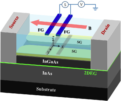
In this work, we consider a finger-gate (FG) controlled narrow constrictionTang2012 ; Loss2014 in the presence of a RZ subband gap, in which a very asymmetric structure in the 2DEG leads to strong SO coupling with the result that the Rashba effect is dominant. The Dresselhaus effect due to BIA is also considered. Below, the SFG and DFG controlled spin-resolved electronic transport properties will be compared in an external in-plane magnetic field as shown in Fig. 1.
The organization of the rest of this paper is as follows. In Sec. II we describe the propagation-matrix approach of tunneling through a DFG system under in-plane magnetic field. In Sec. III we present our calculated results on the spin-split subband structure and the spin-resolved conductance. A concluding remarks is given in Sec. IV.
II spin electronic transport model
In this section, we show that the RZ and RD-Z effects, described by a Hamiltonian technique lead to, respectively, symmetric and asymmetric spin-split subband structures. In addition, the SFG and DFG influence on the transport through the SG confined quantum channel will be described by a spin-dependent PM method.
As is illustrated for the device in Fig. 1, a two dimensional electron gas (2DEG) is induced in an InAs-In1-xGaxAs semiconductor heterojunction grown in the crystallographic direction and is subjected to a split-gate voltage. A pair of split-gates restricts the movement of the electrons of the 2DEG, and therefore a quantum channel is generated in the direction. Propagating electrons in the channel are driven from source to drain.
In the absence of the finger gates, a transported electron is affected by the Rashba effect due to SIA and the Zeeman effect induced by an external in-plane magnetic field, described by the unperturbed Hamiltonian
| (2) |
The first term describes a bare quantum channel that is described by the ideal Hamiltonian
| (3) |
The first term is the kinetic energy of an electron in the 2DEG, where is the reduced Planck constant. A conduction electron has an assigned wave number satisfying and is its effective mass. The second term indicates a split-gate induced confining potential energy that can be modeled by a hard-wall confinement with width for simplicity.
In the second term of Eq. (2), we consider a crystallographic 2DEG system, and hence the Rashba SO Hamiltonian coupling the Pauli spin matrix to the momentum can be reduced to a -linear form
| (4) |
| (5) |
where the Rashba coupling strength is proportional to the electric field along the direction perpendicular to the 2DEG.Nitta1997 The fourth term in Eq. (2) describes an applied external in-plane magnetic field that is selected to be antiparallel to the channel in the direction and has the form (). The longitudinal in-plane magnetic field induces a Zeeman term that can be expressed as
| (6) |
in which indicates half of the effective gyromagnetic factor ( for InAs) and is the Bohr magneton.
Tuning the switch shown in Fig. 1 allows us to investigate SFG and DFG controlled spin-resolved transport properties. We consider the width of the finger-gate scattering potential, , to be less than the Fermi wave length nm and to be described by a delta potential. In addition, we assume a high-mobility semiconductor materials so that impurity effects can be neglected. A FG array system can generally be described by the scattering potential energy
| (7) |
where indicates a delta potential energy induced by the FG , and is the number of FG. For example, = 1 and 2 indicate, respectively, SFG or DFG systems. These FG array systems under the influence of the RD-Z effects can be formally described by the Schrödinger equation
| (8) |
The eigenfunction in Eq. (8) can be obtained by summing over all occupied subbands, , for the product of the spatial wave functions and the spin states, given by
| (9) |
Here the ideal transverse wave function in subband is , in which the subband energy with the quantized wave number .
For simplicity, we employ the Fermi-level in a 2DEG as an energy unit, namely = = with and being, respectively, the effective mass of an electron and the reduced Planck constant. In addition, one selects the inverse wave number as a length unit, namely . Correspondingly, the magnetic field is in units of , and the Rashba SO-coupling constant is in units of . In the following we consider a sufficient narrow channel by assuming the channel width nm so that the bare subband energy is simply . The energy dispersion can thus be expressed as
| (10) |
where indicates the upper () and lower () spin branches. Sufficiently low temperature or K is required to avoid thermal broadening effects.
In order to investigate the SFG and DFG controlled spin-resolved electronic transport properties, we shall explore how the spin-mixing effect due to the interplay of the RD-Z effects influences the propagating and evanescent modes. For a given incident electron energy in the subband , the energy dispersion is related to complex wave number that obeys
| (11) |
To proceed, one has to label the four longitudinal wave numbers as the right-going and left-going , in which the notation indicates spin-up mode and stands for spin-down mode.
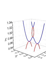
Below, we focus on a sufficiently narrow quantum channel to explore the first two conductance steps associated with the two spin branches of a transported electron occupying the lowest subband. We calculate the quantum transport properties by using a generalized PM method, in which the spin-flip scattering mechanisms is taken into account. The energy dispersion shown in Fig. 2(a) essentially divides the energy spectrum into three regimes, namely the low energy regime , the intermediate energy regime , and the high energy regime . In the low and high energy regimes, there are four propagating modes with real and real . It should be noted that there are two propagating and two evanescent modes in the intermediate energy regime or the RZ energy gap region where the evanescent modes manifest a bubble behavior with imaginary wave vectors.Tang2012
The spin-split wave functions around the scattering potential located at can be formally expressed including the spatial and spin parts as
| (14) | |||||
| (17) |
and
| (20) | |||||
| (23) |
where and indicate the coefficients of right-going electrons with positive group velocity and wave number , while and stand for the coefficients of the left-going electrons with negative group velocity and wave number . There are two boundary conditions around , given by
| (24a) | ||||
| (24b) | ||||
Taking into account the possible incident spin states and allows us to formulate the total PM in an arbitrary FG array system.
| (25) |
or expressed explicitly
| (26) |
Here, the diagonal and off-diagonal terms in and indicate, respectively, the spin-preserve (SP) and spin-flip (SF) reflection and transmission coefficients. The first subscript is the incident spin state, and the second one is the scattered spin state.
To proceed, one has to consider both the and spin states incident from the source electrode. The PM for the electrons with two spin states in the -th region can be expressed as , in which is the PM through the FG and is the free space PM between the FG and . Hence, the total PM for SFG and DFG can be simply expressed as and . In addition, if , or identically zero if , in which and are right-going wave vectors, while and are left-going wave numbers. Solving the PM equation numerically, we may obtain the reflection and transmission coefficients of the scattered intermediate and final states through the SFG or DFG systems.
We consider an electron injected from the left reservoir (source electrode) and transported to the right reservoir (drain electrode) for a given incident energy. Solving for the spin non-flip and flip reflection coefficients and , as well as the spin non-flip and flip transmission coefficients and , we can calculate numerically the conductance based on the Landauer-Büttiker frameworkLandauer1970 ; Buttiker1990
| (27) |
Here = is the conductance quantum per spin state, and and indicate, respectively, the spin branches of the incident and transmitted waves in the left and right leads. Therefore, and represent the group velocity of corresponding modes in the left and right reservoirs, respectively.
III Numerical Results
Calculations presented below are carried out under the assumption of a 2DEG at a high-mobility InAs-In1-xGaxAs semiconductor interface with an electron effective mass and typical electron density cm-2.Nitta1997 Accordingly, the energy unit is = 66 meV, the length unit = 5.0 nm, the magnetic field unit kT, and the spin-orbit coupling parameter is in units of = 330 meVnm. In addition, we assume that the width of the finger gate is = such that the FG potential energy = is in units of meV. Below, we assume that = = for simplicity. By using the above units, all physical quantities presented below are dimensionless.Tang2012
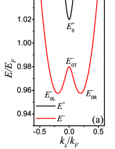
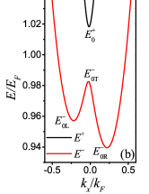
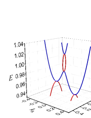
Our previous work has demonstrated that the interplay of the SO interaction and the Zeeman effect may generate a SO-Z gap due to the orthogonality of the SO effective magnetic field and the in-plane magnetic field.Tang2015 In Fig. 2, we show the energy spectrum of the lowest subband. The chosen parameters correspond to a strong SO coupling regime with SO-Z gap. The transported spin-resolved electrons can thus be separated into the low-energy (), the SO-gap (), and the high-energy () regimes. Figure 2(a)-(b) indicates two spin-state energies for a given wave number obtained from Eq. (10), while Figure 2(c)-(d) displays four complex wave numbers for a given electron energy obtained from Eq. (11).
Concerning the Rashba-Zeeman (RZ) effect, Fig. 2(a) shows that the subband bottom energy of the spin-up branch is at = = 1.02, and the subband top energy of the spin-down branch is = = 0.98. Hence, the RZ gap = = = 0.04. This is exactly the Zeeman gap . In addition, the left and right spin-down subband bottoms are at the same energy, namely .
Concerning the Rashba-Dresselhaus-Zeeman (RDZ) effect (), Fig. 2(b) shows that spin-up subband bottom becomes slightly lower ( = 1.018), and the spin-down subband top becomes slightly higher ( = 0.982). Hence, the RDZ gap = 0.036 is smaller than the RZ gap by 0.004. Moreover, the left and right spin-down subband bottoms are no longer the same, that is, and . Below, we shall show that these asymmetric subband bottoms may lead to interesting transport properties.
In order to explore the spin-resolved transport properties, it is important to define the group velocity of an electron in the spin branch
| (28) |
Defining the velocity allows us to determine a local minimum and a maximum in the subband structures by setting the group velocity identically zero.
Without the Dresselhaus effect, the two subband bottoms in the lower spin branch can be analytically obtained at corresponding to the same subband bottom energy = = . With the Dresselhaus effect, this degeneracy subband bottom will be broken as is shown in Fig. 2(b). Fig. 2(c) and (d) show their corresponding energy dispersion with respect to complex that is important to perform transport calculation.
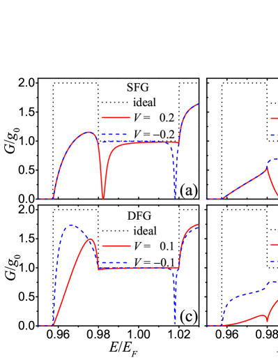
In Fig. 3, we compare the conductance behavior of SFG and DFG systems with no Dresselhaus effect. The conductance in the SFG system shown in Fig. 3 (a) and (b) reveals a perfect mirror effect between the electron-like QBS (EQBS) for negative and hole-like QBS (HQBS) for positive . Moreover, the QBS dips for become the QBS valleys for . This indicates that a stronger voltage results in a shorter QBS life time.
It is interesting to compare the SFG with voltage to a DFG with voltage and keep the two FGs very close, say with , as shown in Fig. 3 (c) and (d). It is surprising that the EQBS structures in the DFG and the SFG system at a negative are almost unchanged, but the HQBS structures are very different. Fig. 3(c) demonstrates that a weak positive voltage () in the DFG system does not allow a formation of a HQBS. If the voltage is increased to 0.3, the HQBS valley in SFG becomes a dip around and a Fano dip in the SO-Z gap as shown in Fig. 3(d).
.
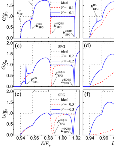
In Fig. 4, we show the conductance of SFG and DFG systems as a function of electronic energy in the presence of Dresselhaus SO interaction for = (a)-(b) ; (c)-(d) ; and (e)-(f) . The other parameters and , satisfying + , are within the strong SO coupling regime.
In the case of a SFG, sufficient low energy with negative FG voltage may result in a Fano line-shape (see Fig. 4(a) and (c)). This is due to the interference between the SFG BS below the left spin-down bottom and the extended state at the right spin-down branch. The binding energy of the SFG BS can be analytically predicted to be = = 0.0025 () and 0.01 (), as shown by solid blue lines. This binding energy can also be numerically determined using
| (29) |
with = 0.957, while = 0.9545 () and 0.9468 (). We thus numerically obtain the SFG BS binding energy = 0.0026 () and 0.0103 () that is approximately the same as our analytical prediction delivers.
If the incident electron energy is within the gap region, the mirror effect between the HQBS and EQBS is clearly shown in the SFG system. More precisely, the SFG HQBS energies = 0.9831, 0.9843, 0.9857 for = 0.1, 0.2, 0.3, respectively, are slightly above the spin-down top energy = 0.982. Accordingly, the SFG EQBS energies = 1.0178, 1.0168, 1.0153 for = , respectively, are slightly below the spin-up bottom energy = 1.018. The higher may slightly shift the HQBS and EQBS toward the center of the SO-Z gap.
In the case of a DFG shown in Fig. 4, a sufficient low energy = 0.957 with a negative FG potential may result in a sharp peak (see Fig. 4(b)) corresponding to a DFG BS energy = 0.9501 below . The DFG BS binding energy can be numerically obtained
| (30) |
giving = 0.0069 in units of .
In order to provide an evidence of such a DFG BS mechanism, we derive an analytical expression for , given by
| (31) |
This equation allows us to analytically estimate the binding energy = for and . This is only a bit smaller than our numerical result.
Comparing Figs. 4(b), (d), and (f), we see that if the DFG potential is negatively increased, the electron-like QBS (EQBS) dip is red shifted towards the center of the SO-Z gap and becomes more significant. If , as is shown in Fig. 4(d), the DFG binding energy as can be estimated from Eq. (31), the corresponding BS energy is below the subband threshold . The DFG BS thus disappears in Fig. 4(d) as well as Fig. 4(f). On the contrary, increasing the positive DFG potential (), the HQBS dip around the subband top becomes a blue shifted broad valley, as shown by the dashed red lines in Figs. 4(b), (d) and 4(f). These HQBS dips are at and , respectively. The shift of the location of the HQBS is if the DFG potential is increased by .
.
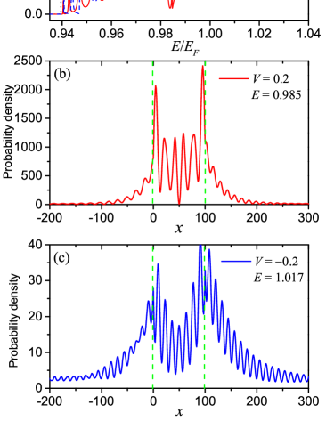
In order to demonstrate the possibility of forming a resonant state (RS) in a DFG system, we consider the system with a long FG distance, = . The corresponding conductance is plotted as a function of energy shown in Fig. 5(a). When the gate voltage is (short dashed line), the conductance manifests a clear EQBS resonance dip at energy = . However, for a positive gate voltage (solid line) the conductance displays a more complicated structure. There is a broad resonance leading to a valley structure around = corresponding to a HQBS with a binding energy approximately 0.0014.
More importantly, when , a RS peak is found in the conductance around = caused by multiple scattering between the two fingers leading to a resonant transmission. The corresponding energy can be estimated using an infinite quantum well model with a zero point energy measured from the subband top of the lower spin branch .
| (32) |
in which = , and hence we obtain .
The probability densities shown in Figure 5(b)-(c) () are typical for resonances formed between finger gates. They are localized in the gate region, and due to the considerable length of the system () the interference caused by the fingers is well visible as oscillations of the probabilities densities.
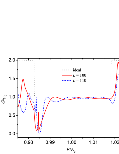
In order to provide further evidence that the peak at the energy , for gate potential and distance between the fingers (shown by red solid line in Fig. 5(a)) is a RS caused by multiple scattering we test its length dependence. We compare with results for shown by a dashed blue curve in Fig. 6. The RS peak in the case of is at that is lower than for and in accordance with what is to be expected. The dependence on the distance between the two fingers in the DFG system allows us to identify the sharp peaks in the conductance as a RS feature.
IV Concluding Remarks
In conclusion, We have developed a model to investigate the interplay of the strong SO coupling and the Zeeman effect, in which the lower spin branch contains a local band top in reciprocal space forming a SO-Z gap. We have demonstrated that this particular subband structure in SFG and DFG systems leads to interesting spin-resolved electronic transport properties.
In the absence of the Dresselhaus effect, the spin-split subband structure is symmetric with respect to the wave vector resulting in a degeneracy of the subband threshold. In this case, we identify the physical mechanisms responsible for the appearance for conductance mirror effect between the HQBS and EQBS in a SFG system. However, in a DFG system, the HQBS caused by a positive FG potential is strongly suppressed, but the EQBS feature remains significant.
In the presence of the Dresselhaus interaction, the subband structure becomes asymmetric with respect to the wave vector. We successfully predict the binding energy of the real BS in the lower spin branch for both the SFG and the DFG systems. Especially, a RS can be found in a DFG system that is localized in the finger region due to multiple scattering. Our theoretical prediction of a formation of a BS and an RS mechanisms gives a hint for a design of a SO-Z based spin electronic device.
Acknowledgements.
This work was supported by the MOST in Taiwan through Contract No. 103-2112-M-239-001-MY3, the Icelandic Research and Instruments Funds, and the Research Fund of the University of Iceland.References
- (1) D. Loss and D. P. Divincenzo, Phys. Rev. A 57, 120 (1998).
- (2) I. utić, J. Fabian, and S. Das Sarma, Rev. Mod. Phys. 76, 323 (2004).
- (3) S. A. Wolf, D. D. Awschalom, R. A. Buhrman, J. M. Daughton, S. von Molnr, M. L. Roukes, A. Y. Chtchelkanova, and D. M. Treger, Spintronics: A Spin-Based Electronics Vision for the Future, Science 294, 1488 (2001).
- (4) Semiconductor Spintronics and Quantum Computation, edited by D.D. Awschalom, N. Samarth, and D. Loss (Springer-Verlag, Berlin, 2002).
- (5) D. D. Awschalom and M. E. Flatte, Nat. Phys. 3, 153 (2007).
- (6) S. Heedt, C. Morgan, K. Weis, D. E. Brgler, R. Calarco, H. Hardtdegen, D. Grtzmacher, and T. Schpers, Nano Lett. 12, 4437 (2012).
- (7) E. I. Rashba, Sov. Phys. Solid State 2, 1109 (1960); Y. A. Bychkov and E. I. Rashba, J. Phys. C 17, 6039 (1984).
- (8) R. Winkler, Spin-Orbit Coupling Effects in Two-Dimensional Electron and Hole Systems, Springer Tracts in Modern Physics Vol. 191 (Springer, Berlin, 2003).
- (9) L. Meier, G. Salis, I. Shorubalko, E. Gini, S. Schon, and K. Enslin, Nat. Phys. 3, 650 (2007).
- (10) S. Bandyopadhyay and M. Cahay, Appl. Phys. Lett. 85, 1814 (2004).
- (11) H. C. Koo, J. H. Kwon, J. H. Eom, J. Y. Chang, S. H. Han, and M. Johnson, Science 325, 1515 (2009).
- (12) A. F. Sadreev and E. Ya. Sherman, Phys. Rev. B 88, 115302 (2013).
- (13) K. E. Nagaev and A. S. Goremykina, Phys. Rev. B 89, 035436 (2014).
- (14) C.-S. Tang, S.-T. Tseng, V. Gudmundsson, and S.-J. Cheng, J. Phys.: Cond. Mat. 27, 085801 (2015).
- (15) J. Nitta, T. Akazaki, H. Takayanagi, and T. Enoki, Phys. Rev. Lett. 78, 1335 (1997).
- (16) E. R. Mucciolo, C. Chamon, and C. M. Marcus, Phys. Rev. Lett. 89, 146802 (2002); S. K. Watson, R. M. Potok, C. M. Marcus, and V. Umansky, ibid. 91, 258301 (2003).
- (17) A. Brataas, Y. Tserkovnyak, G. E. W. Bauer, and B. I. Halperin, Phys. Rev. B 66, 60404 (2002).
- (18) P. Zhang, Q. K. Xue, and X. C. Xie, Phys. Rev. Lett. 91, 196602 (2003).
- (19) B. G. Wang, J. Wang, and H. Guo, Phys. Rev. B 67, 092408 (2003).
- (20) L. Serra, D. Sánchez,1 and Rosa López, Phys. Rev. B 72, 235309 (2005).
- (21) M. Scheid, D. Bercioux, and K. Richter, New J. Phys. 9, 401 (2007).
- (22) Q. F. Sun, H. Guo, and J. Wang, Phys. Rev. Lett. 90, 258301 (2003).
- (23) W. Zeng, J. L. Wu, B. G. Wang, J. Wang, Q. F. Sun, and H. Guo, Phys. Rev. B 68, 113306 (2003).
- (24) Y. V. Pershin, J. A. Nesteroff, and V. Privman, Phys. Rev. B 69, 121306(R) (2004).
- (25) C. H. L. Quay, T. L. Hughes, J. A. Sulpizio, L. N. Pfeiffer, K.W. Baldwin, K.W.West, D. Goldhaber-Gordon, and R. de Picciotto, Nat. Phys. 6, 336 (2010).
- (26) P. Zhang, Z.-L. Xiang, and F. Nori, Phys. Rev. B 89, 115417 (2014).
- (27) G. Dresselhaus, Phys. Rev. 100, 580 (1955).
- (28) C.-S. Tang, S. Y. Chang, and S. J. Cheng, Phys. Rev. B 86, 125321 (2012).
- (29) D. Rainis and D. Loss, Phys. Rev. B 90, 235415 (2014).
- (30) R. Landauer, Philos. Mag. 21, 863 (1970).
- (31) M. Büttiker, Phys. Rev. B 41, 7906 (1990).