Understanding magnetic focusing in graphene p-n junctions through quantum modeling
Abstract
We present a quantum model which provides enhanced understanding of recent transverse magnetic focusing experiments on graphene p-n junctions. Spatially resolved flow maps of local particle current density show quantum interference and p-n junction filtering effects which are crucial to explaining the device operation. The Landauer-Büttiker formula is used alongside dephasing edge contacts to give exceptional agreement between simulated non-local resistance and the recent experiment by Chen et al (Science, 2016). The origin of positive and negative focusing resonances and off resonance characteristics are explained in terms of quantum transmission functions. Our model also captures subtle features from experiment, such as the previously unexplained - to - transition and the second p-n focusing resonance.
I Introduction
Traditionally, transverse magnetic focusing (TMF) experiments have been restricted to unipolar conduction, in mediums such as metals Tsoi and Tsoi (1978) and two-dimensional electron gasses (2DEG) van Houten et al. (1989). The discovery of graphene Novoselov et al. (2004), in which electrons behave as massless Dirac fermions Novoselov et al. (2005), has provided an exciting new platform for studying TMF. Graphene’s gapless band structure, allowing ambipolar conduction, has enabled several recent TMF experiments. TMF in graphene has been studied as a function of carrier density Taychatanapat et al. (2013) and imaged with scanning gate microscopy Bhandari et al. (2016). In addition, a large number of TMF peaks have been observed in graphene/hexagonal boron nitride superlattices Lee et al. (2016). Recently, p-n junctions in graphene have been used in TMF experiments to steer the focused beam Chen et al. (2016), opening the door to new electron optics. The p-n junction is a fundamental device and has received a significant amount of attention from the graphene community. Graphene p-n junctions have rich physical properties, exhibiting chiral tunneling Katsnelson et al. (2006); Young and Kim (2009), angle dependent transmission Cheianov and Fal’ko (2006); Sutar et al. (2012); Sajjad et al. (2012), quantized conductance in high magnetic fields Abanin and Levitov (2007); Williams et al. (2007); Klimov et al. (2015), and ballistic interference Rickhaus et al. (2013).
In this paper, we use quantum transport methods to model the graphene p-n junction TMF experiment of Chen et al Chen et al. (2016). Our calculations, implemented in the KWANT package Groth et al. (2014), intrinsically capture quantum interference, tunneling, and angle dependent transmission Low and Appenzeller (2009), which enables us to explain the results of Chen et al Chen et al. (2016) in a completely quantum mechanical framework, without any fitting parameters. Previously, we have used the same basic model to understand quantum Hall measurements in graphene p-n junctions LaGasse and Lee (2016). By including large dephasing edge contacts and performing multi-terminal Landauer-Büttiker analysisBüttiker (1988), we are able to capture both the in-resonance and off-resonance characteristics of the device. We achieve exceptionally strong agreement between our simulation and experiment Chen et al. (2016), as shown in Fig. 7.
When a magnetic field is applied perpendicular to a graphene p-n junction, electrons transporting across the junction will form snake states, arcing between the p and n sides of the junction Beenakker (2008). In graphene, the arcs are characterized by the cyclotron radius, given by with the reduced Planck’s constant, the carrier density, the electron charge, and the applied magnetic field. Snake states have been observed along graphene p-n junctions in several experiments Williams and Marcus (2011); Rickhaus et al. (2015); Taychatanapat et al. (2015). Additionally, transport of electrons in snake states has been modeled using quantum mechanicalRickhaus et al. (2015); Zarenia et al. (2013); Milovanović et al. (2014a); Kolasiński et al. (2016) and semi-classical Carmier et al. (2010, 2011); Patel et al. (2012); Davies et al. (2012); Milovanović et al. (2013); Milovanović et al. (2014b) methods.
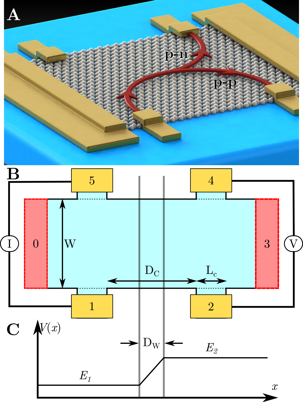
The TMF experiment performed on graphene p-n junctions by Chen et al Chen et al. (2016) probes a special case of snake state transport, in a device similar to that depicted in Figures 1a and 1b. The device studied by Chen et al Chen et al. (2016) is special because the distance between contacts on each side of the junction, , is approximately equal to the width of the device, . When , the applied magnetic field focuses electrons directly between the contacts. In a unipolar system the carriers are directed back to the side from which they originate. Conversely, in a junction, the carriers will be steered towards the opposite side of the device. These two paths are depicted in Fig 1a.
II Transport Model
In this paper, we study a tight-binding Hamiltonian describing low energy electrons in graphene, given by
| (1) |
where the second summation only takes place for atoms which are first nearest-neighbors. are Fermionic creation/annihilation operators, is the on-site energy at site i, and is the hopping energy between sites i and j. The effect of an applied magnetic field is included using Peierl’s substitution, , where we adopt a circular gauge for the vector potential A Shevtsov et al. (2012). We use a scaled tight-binding modelLiu et al. (2015) where . The term scales the lattice constant, , and the atomistic hopping energy , eVReich et al. (2002), to yield more efficient simulations.
We simulate a six terminal Hall bar, as depicted in Fig 1b, with four small contacts (labeled one, two, four, and five) and two large contacts (labeled zero and three). The spacing between the inner edges of the small contacts is set equal to the width of the Hall bar, , which is the critical element of device design to observe the first p-n focusing peak. To form p-n junctions, the on-site energy on each side of the device may be tuned independently to and . We set the on-site energy to change linearly between and over a junction width, , as shown in the energy band diagram in Fig 1c.
The two large contacts, zero and three, are included as dephasing contacts. The voltages of these contacts are allowed to float in the simulation, accounting for any dephasing which occurs as the carrier wave skips along the left or right side of the device. This type of virtual dephasing contact has been used in quantum transport calculations in the past Stegmann et al. (2013)Stegmann and Lorke (2015) and is critical for tying our results to experiment.
Since most TMF measurements are performed at cryogenic temperatures under very small biases, we adopt a zero-bias, zero-temperature approximation. In this regime, we utilize the Landauer-Büttiker equationBüttiker (1988) to express the current in each lead p Datta (1995),
| (2) |
where the summation takes place over all leads in the system, including the dephasing contacts. For our simulation, (2) generates a system of six linear equations with six unknowns. The term is the quantum mechanical transmission function from lead p to q, defined as
| (3) |
where is the scattering matrix element between the and mode in leads and , respectively. The summation in (3) takes place over the available modes in each lead at energy .
To connect with the multi-terminal measurement of Chen et al Chen et al. (2016), we simulate driving a current between contacts one and five and calculate the voltage acquired by contacts two and four. Practically, this requires setting , , and choosing a contact to be grounded, in this case . The non-local resistance for this configuration is defined as
| (4) |
The components of (4) are attained by solving the linear system, , defined by (2), where and are column vectors of lead currents and voltages, respectively, and is a matrix of transmission functions. Making the substitutions above, (4) may be reduced to . and are elements of the matrix, defined as , and are entirely comprised of transmission functions between different leads, thus, the problem is reduced to calculating the permutations of (3).
To understand the terminal characteristics of our simulation, we generate spatially resolved particle current density maps using
| (5) |
where is the position of the lattice site, is the wave function of the conducting mode in lead p. The summation takes place over all conductive modes in lead p available at energy . However, separately resolving each mode is informative.
III Results and discussion
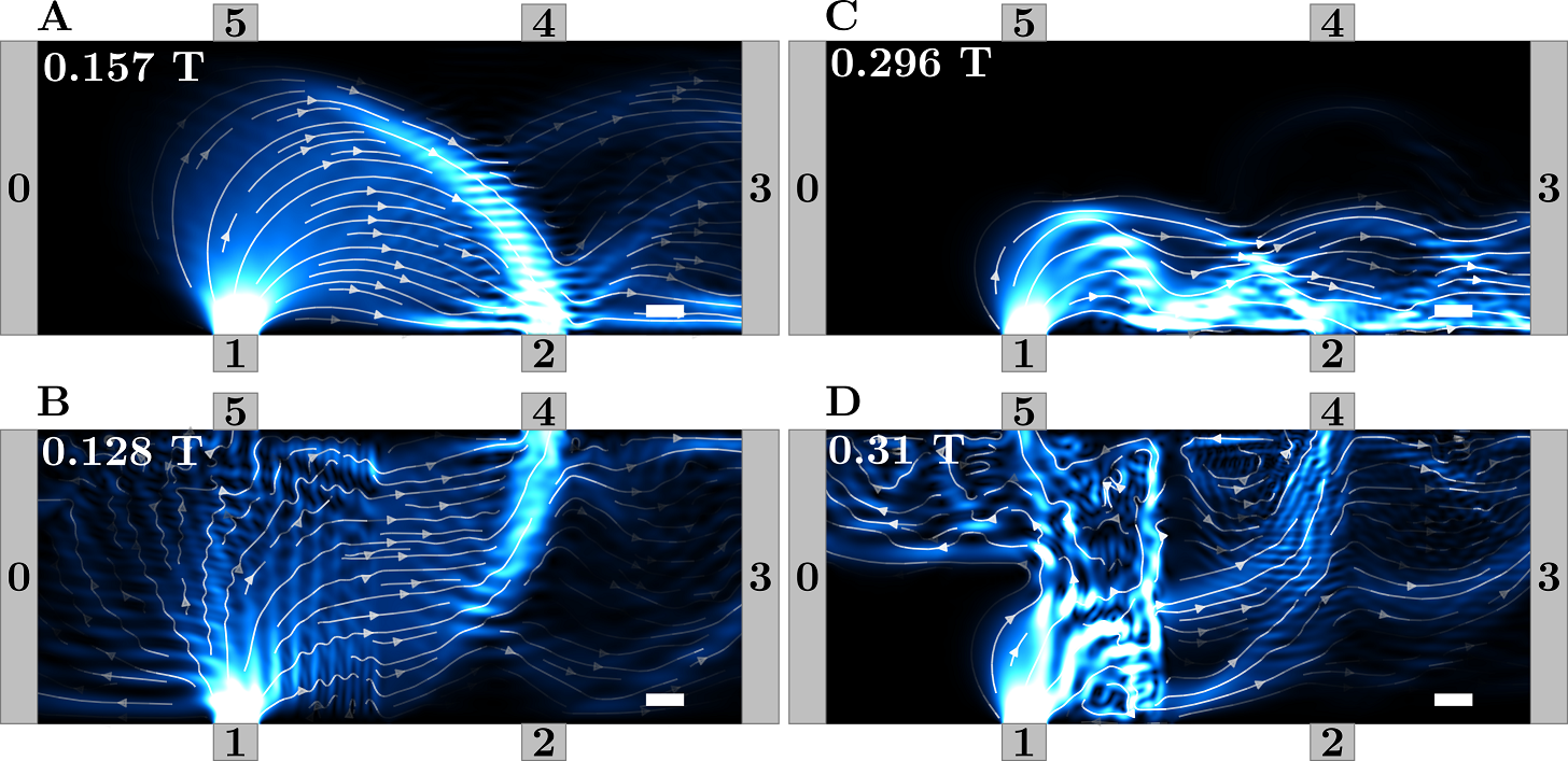
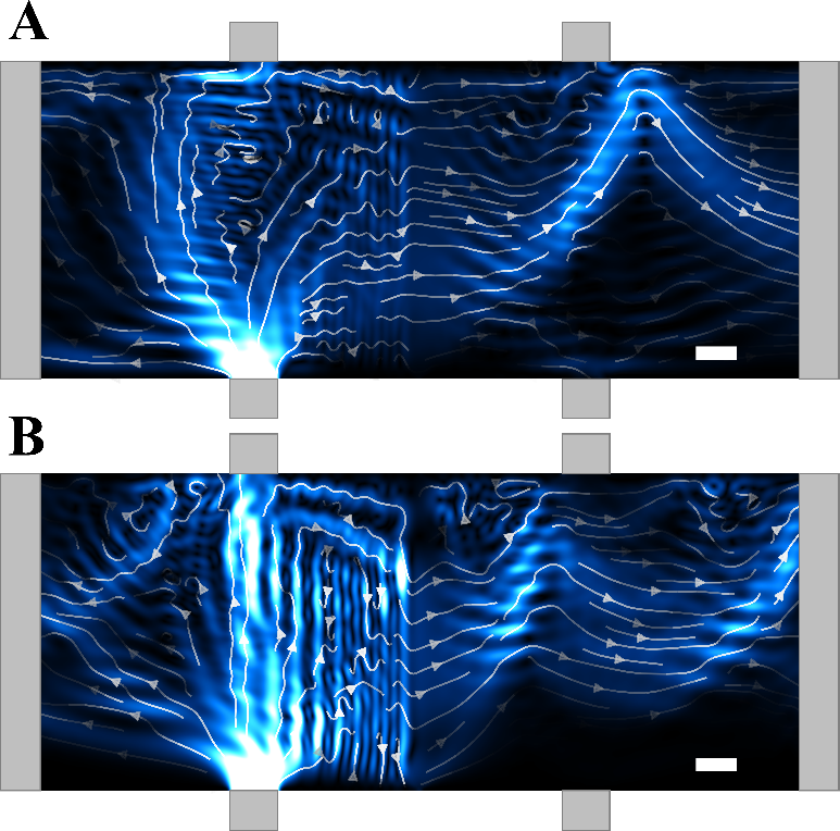
In Fig. 2 we plot vector flow maps of the local particle current density (5) injected by contact one for p-p’ and p-n junctions. When current is focused into contact two/four we observe positive/negative peaks in the non-local resistance, respectively.
When the p-p’ junction is in the first TMF resonance, in Fig. 2a, carriers injected by contact one are focused directly into contact two. The carriers are injected and take on a broad spread of angles in the channel, but are primarily focused into a bright caustic which enters contact two. The junction redirects the carriers slightly, elongating the orbit. Due to the small size of the contacts, not all carriers which are injected by contact one are collected at contact two. Some hit the bottom edge of the device and skip into contact three, from which corresponding interference fringes may be seen, especially on the caustic.
For the first resonance of the p-n junction, in Fig. 2b, current injected from contact one is focused directly into contact four. The 50 nm junction width acts as a low pass filter, allowing only current flowing close to normal to the junction to transmit. On the left side of the junction, wave interference patterns indicate the current density reflected off the junction, which then exits out the contacts on the left side of the device. The transmitted current predominately focuses into a caustic which enters contact four.
At low magnetic fields, a significant portion of the current injected from contact one hits the top edge of the device before crossing the junction, as seen for p-n junction in Fig. 2b. This is a consequence of the device geometry studied by Chen et al Chen et al. (2016) and increasing the device width to avoid hitting the top edge prohibits one from probing the first p-n TMF resonance. Interestingly, a component of the current hitting the top edge is redirected and transmits across the junction. This subtle detail, captured by our model, contributes to the device’s terminal characteristics and is important in many of the different junction configurations.
When the magnetic field is increased to the second TMF resonance, in Fig. 2c and d, the current density will skip along the edge of the junction (p-n case) or the edge of the device (p-p’ case). p-n junctions do not exhibit the second resonance until the n-doping is stronger than the p-doping, thus we configure the junction in Fig. 2d as meV and meV. In the p-n configuration, on the p-side, the current forms a circular orbit which reflects near the bottom of the junction and again almost half way up. At each of these points there is a significant portion of current which is incoming normal to the junction and transmits to the other side, focusing on contact 4. Due to the filtering effect of a smooth p-n junction, the second TMF resonance is significantly weaker.
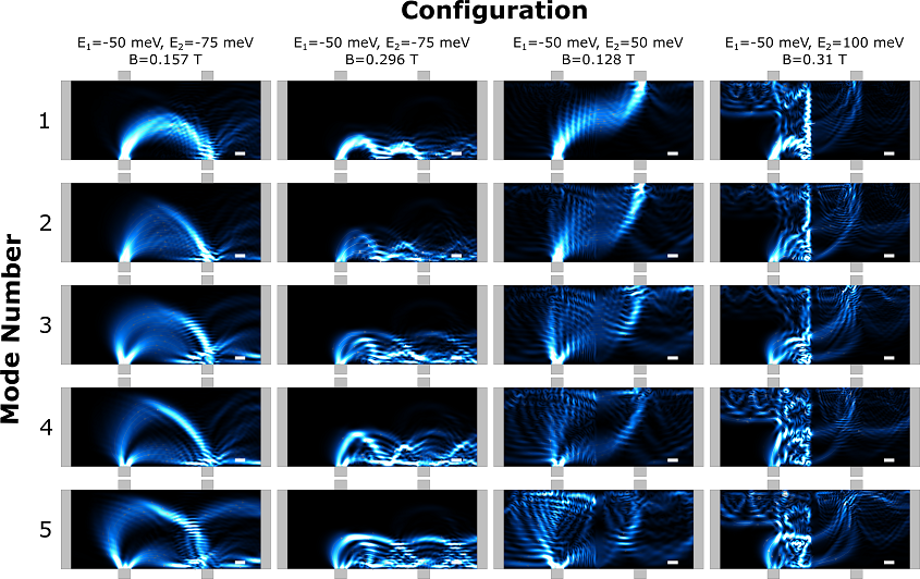
To further understand the local particle current density of the devices in Fig. 2, in Fig. 3 we resolve the characteristic by each propagating mode. By resolving each mode which contributes to the results in Fig. 2, we observe a combination of features reminiscent of semi-classical skipping orbits and quantum mechanical interference patterns.
The lowest mode is injected straight into the device, perpendicular to the semi-infinite contact. In the first resonance of the p-p’ and p-n junction, shown in columns one and three of Fig. 3, respectively, the lowest mode is bent so that the wave is propagating approximately normal to the junction when it crosses it. Thus, the lowest mode is nearly perfectly transmitted, with very few reflections (indicated by interference fringes) visible.
Higher modes are injected into the device with non-zero angles and arrive at the junction traveling at oblique angles. For the first resonance of the p-p’, the beam is noticeably refracted as it crosses the junction. In the p-n junction, the higher order modes have significant components which are reflected off the junction, due to the angle dependent transmission across the junction.
For the second resonance of the p-p’ and p-n’ configurations, the local particle current density patterns in Fig. 2 are more complex than the first resonance. By resolving each mode, we are able to develop a better picture of the important transport mechanisms. The higher order modes for the p-p’ junction have a component which transports nearly parallel to the lower edge of the device. This is particularly evident in the fourth and fifth modes. Most of the carriers which transport in this manner will miss contact two and transmit out contact three, resulting in a weaker signal for the second focusing resonance.
The second focusing resonance of the p-n’ displays the most complex characteristics of the device, with predominant quantum characteristics not present in the other configurations. At the higher magnetic field, the first and second modes appear to begin to form Landau levels when they collide with the junction, similar to what we have studied in our previous work LaGasse and Lee (2016). The higher order modes, however, instead show a more complex, swirling pattern. The carriers transport in skipping orbits which partially reflect of the junction, interfering with themselves. A portion of each orbit transmits across the junction, contributing to the second p-n’ resonance.
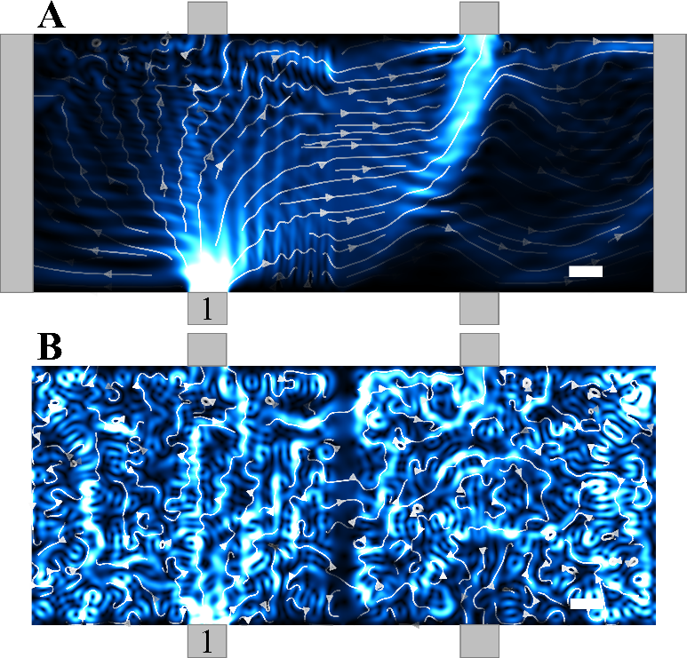
As mentioned previously, the dephasing edge contacts (labeled contact zero and three) are critical to attaining the results presented in this paper. To demonstrate this importance, in Fig. 4 we plot the local particle current density for the device configured as in Fig. 2b both with and without the dephasing contacts. When the dephasing contacts are removed, in Fig. 4b, the portions of the wave which normally exit contacts zero and three, instead scatters around the edge of the device. The wave will continue to scatter around the device, interfering with itself, until exiting out one of the small contacts. This process occurs until the device reaches steady state, resulting in the extremely chaotic pattern shown and the destruction of any resonance characteristics.
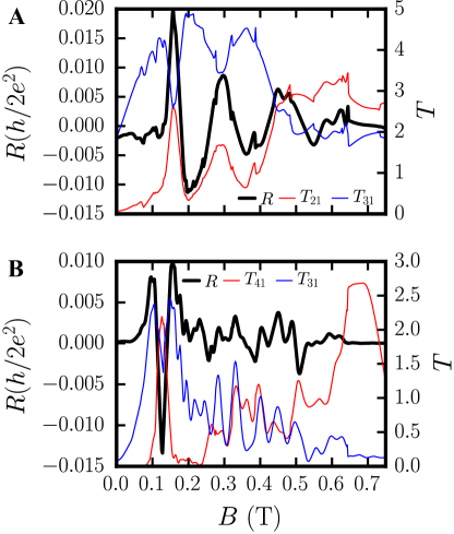
Fig. 5 shows the non-local resistance (4) and selected transmission coefficients (3) as a function of applied magnetic field for an asymmetric p-p’ junction and a symmetric p-n junction. The two junction configurations are doped the same as in Fig. 2a and b, respectively.
It is non-trivial to extract specific terms from (4), in terms of transmission functions, which result in the final form of the non-local resistance. The final magnitude and shape of the curve consists of permutations of transmission functions between every contact combined together. However, we are able to target specific transmission functions which are important in understanding the problem.
In the unipolar p-p’ configuration, we observe three well defined TMF resonances. We are able to match the first two TMF resonances to a peak in the transmission from contact one into two, . When the junction is switched to the p-n configuration, when in resonance, carriers are now focused from contact one into contact four. This results in a negative peak in resistance at T, shown in Fig. 5b. The important transmission function for understanding the resonance condition of the p-n junction is , which is peaked while the device is in resonance.
Each subsequent TMF resonance of the unipolar junction configuration decreases in magnitude. For higher order TMF resonances, an increase in indicates that the focusing effect is diminished. This is due to interference caused by the increased number of scattering events off the edges of the device.
When either configuration of junction is not in resonance, there is an increase in the transmission from contact one into contact three, . In the off-resonance state of the p-p’ junction, carriers which are not focused from contact one into two will hit the bottom edge of the device and skip into contact three. To maintain current conservation, the carriers will be re-injected by the floating contact three and the magnetic field will direct the carriers towards contact four, resulting in the negative off-resonance resistance in Fig. 5a. Conversely, in the p-n junction, carriers which miss contact four will skip along the top edge of the device. Again, they will be dephased by contact three, except this time the re-injected carriers will be directed towards contact two, which results in the positive off-resonance resistance in Fig. 5b. In Fig. 6 we illustrate the off-resonance particle current density for a symmetric p-n junction.
The junction filtering effect, seen in Fig. 2, results in significantly weaker and fewer TMF resonances when the device is in the p-n configuration. For the symmetric p-n junction, in Fig. 5, only a single well defined resonance is observed. At higher magnetic fields the beam of carriers skips along the edge of the junction; each time the beam hits the junction only a very small amount will leak through. Since, in our model, no dephasing happens along the junction, the reflected wave of carriers will interfere with itself, further disrupting any resonance from setting up.
In addition, the non-local resistance tends towards zero for each configuration at around T. This is due to the carriers being forced into edge states as the device enters the quantum Hall regime. This effect is also the reason why we do not see a well defined peak in for the third TMF resonance of the p-p’ junction configuration. Capturing this feature highlights the power of quantum transport modeling, where our simulations smoothly transition between carriers occupying semi-classical skipping orbits and edge states.
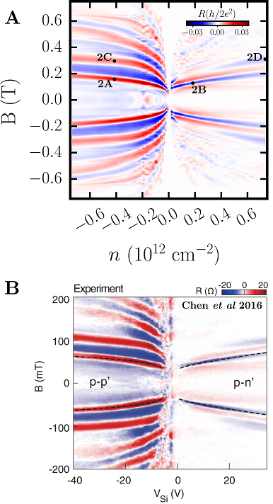
Finally, in Fig. 7, we compare our model with the recent experimental data of Chen et al Chen et al. (2016), reproduced with copyright permission. In Fig. 7a, we fix the doping of the left side of the junction to meV (p-type) and vary the doping of the right side of the junction and applied magnetic field simultaneously. For each configuration we calculate the non-local resistance (4) as before. We report the doping of the right side in terms of carrier density , which has a similar functional form to the gate voltage applied in experiment.
Our simulation results show a striking similarity to the experimental data, capturing all of the major features. These include the four unipolar junction TMF resonances, the first ambipolar TMF resonance, and the negative/positive peaks in resistance when the unipolar/ambipolar configurations are not in resonance, respectively.
We also are able to explain a number of subtle features seen experimentally which are due to the transitions between different types of junctions. The second negative peak in the unipolar junction configuration begins to disappear as the right side of the device is more strongly doped p-type. This transition occurs when the doping of the right side of the junction exceeds the doping of the left side.
The second ambipolar junction TMF resonance in Fig. 7 is extremely weak until the n-type doping of the right side of the junction exceeds the fixed p-type doping. This effect is enabled by the increased number of modes available to conduct on the right side of the junction as the doping is increased. The filtering effect due to the large junction width present in our model and in experiment Chen et al. (2016) prohibits the traditional picture of the carrier density snaking across the junction several times in the second TMF resonance. Instead, the resonance has the characteristic of the flow map shown in Fig. 2d.
In our simulation a larger magnetic field must be used, since our simulated Hall bar is about a factor of ten smaller than the experimental device. The difference in device size and contact dimensions also accounts for the difference in magnitude of our simulated resistance. Using larger contacts will result in smaller values of resistance. However, the concepts we have discussed may still be applied to understand the experimental measurements of Chen et al Chen et al. (2016).
IV Conclusion
In conclusion, we demonstrate a quantum transport model for a TMF experiment on graphene p-n by Chen et al Chen et al. (2016). Spatially resolved particle current density flow maps reveal the behavior of carriers in the first and second resonances of p-p’ and p-n junctions. Our results demonstrate the importance of wave interference and junction filtering effect for understanding TMF experiments. A combination of dephasing edge contacts and use of the Landauer-Büttiker formula supplementing the standard tight-binding model yield extremely close agreement with experiment. Our non-local resistance simulations show well defined positive and negative peaks, which are due to enhanced transmission into contacts three or four, respectively. Many of the features seen by Chen et al Chen et al. (2016) have been explained, including the transition into the quantum Hall regime for high magnetic fields and the transitions between different p-p’ and p-n doping regimes.
Acknowledgements.
The authors acknolwedge financial support provided by the U.S. Naval Research Laboratory (Grant Number: N00173-14-1-G017).References
- Tsoi and Tsoi (1978) V. S. Tsoi and N. Tsoi, Jetp 1962, 150 (1978).
- van Houten et al. (1989) H. van Houten, C. W. J. Beenakker, J. G. Williamson, M. E. I. Broekaart, P. H. M. van Loosdrecht, B. J. van Wees, J. E. Mooij, C. T. Foxon, and J. J. Harris, Physical Review B 39, 8556 (1989).
- Novoselov et al. (2004) K. S. Novoselov, A. K. Geim, S. V. Morozov, D. Jiang, Y. Zhang, S. V. Dubonos, I. V. Grigorieva, and A. A. Firsov, Science 306, 666 (2004).
- Novoselov et al. (2005) K. S. Novoselov, A. K. Geim, S. V. Morozov, D. Jiang, M. I. Katsnelson, I. V. Grigorieva, S. V. Dubonos, and A. A. Firsov, Nature 438, 197 (2005).
- Taychatanapat et al. (2013) T. Taychatanapat, K. Watanabe, T. Taniguchi, and P. Jarillo-Herrero, Nature Physics 9, 225 (2013).
- Bhandari et al. (2016) S. Bhandari, G.-H. Lee, A. Klales, K. Watanabe, T. Taniguchi, E. Heller, P. Kim, and R. M. Westervelt, Nano Letters 16, 1690 (2016).
- Lee et al. (2016) M. Lee, J. R. Wallbank, P. Gallagher, K. Watanabe, T. Taniguchi, V. I. Fal’ko, and D. Goldhaber-Gordon, Science 353, 1526 (2016).
- Chen et al. (2016) S. Chen, Z. Han, M. M. Elahi, K. M. M. Habib, L. Wang, B. Wen, Y. Gao, T. Taniguchi, K. Watanabe, J. Hone, A. W. Ghosh, and C. R. Dean, Science 353, 1522 (2016).
- Katsnelson et al. (2006) M. I. Katsnelson, K. S. Novoselov, and A. K. Geim, Nature Physics 2, 620 (2006).
- Young and Kim (2009) A. F. Young and P. Kim, Nature Physics 5, 222 (2009).
- Cheianov and Fal’ko (2006) V. V. Cheianov and V. I. Fal’ko, Physical Review B 74, 041403 (2006).
- Sutar et al. (2012) S. Sutar, E. S. Comfort, J. Liu, T. Taniguchi, K. Watanabe, and J. U. Lee, Nano Letters 12, 4460 (2012).
- Sajjad et al. (2012) R. N. Sajjad, S. Sutar, J. U. Lee, and A. W. Ghosh, Phys. Rev. B 86, 155412 (2012).
- Abanin and Levitov (2007) D. A. Abanin and L. S. Levitov, Science 317, 641 (2007).
- Williams et al. (2007) J. R. Williams, L. DiCarlo, and C. M. Marcus, Science 317, 638 (2007).
- Klimov et al. (2015) N. N. Klimov, S. T. Le, J. Yan, P. Agnihotri, E. Comfort, J. U. Lee, D. B. Newell, and C. A. Richter, Physical Review B 92, 241301 (2015).
- Rickhaus et al. (2013) P. Rickhaus, R. Maurand, M.-H. Liu, M. Weiss, K. Richter, and C. Schönenberger, Nature Communications 4, 2342 (2013).
- Groth et al. (2014) C. W. Groth, M. Wimmer, A. R. Akhmerov, and X. Waintal, New Journal of Physics 16, 063065 (2014).
- Low and Appenzeller (2009) T. Low and J. Appenzeller, Physical Review B - Condensed Matter and Materials Physics 80, 1 (2009).
- LaGasse and Lee (2016) S. W. LaGasse and J. U. Lee, Phys. Rev. B 94, 165312 (2016).
- Büttiker (1988) M. Büttiker, Physical Review B 38, 9375 (1988).
- Beenakker (2008) C. W. J. Beenakker, Reviews of Modern Physics 80, 1337 (2008).
- Williams and Marcus (2011) J. R. Williams and C. M. Marcus, Physical Review Letters 107, 046602 (2011).
- Rickhaus et al. (2015) P. Rickhaus, P. Makk, M.-H. Liu, E. Tóvári, M. Weiss, R. Maurand, K. Richter, and C. Schönenberger, Nature Communications 6, 6470 (2015).
- Taychatanapat et al. (2015) T. Taychatanapat, J. Y. Tan, Y. Yeo, K. Watanabe, T. Taniguchi, and B. Özyilmaz, Nature Communications 6, 6093 (2015).
- Zarenia et al. (2013) M. Zarenia, J. M. Pereira, F. M. Peeters, and G. A. Farias, Physical Review B 87, 035426 (2013).
- Milovanović et al. (2014a) S. P. Milovanović, M. Ramezani Masir, and F. M. Peeters, Applied Physics Letters 105, 123507 (2014a).
- Kolasiński et al. (2016) K. Kolasiński, A. Mreńca-Kolasińska, and B. Szafran, ArXiv e-prints (2016), arXiv:1610.07566 [cond-mat.mes-hall] .
- Carmier et al. (2010) P. Carmier, C. Lewenkopf, and D. Ullmo, Physical Review B 81, 241406 (2010).
- Carmier et al. (2011) P. Carmier, C. Lewenkopf, and D. Ullmo, Physical Review B 84, 195428 (2011).
- Patel et al. (2012) A. A. Patel, N. Davies, V. Cheianov, and V. I. Fal’ko, Phys. Rev. B 86, 081413 (2012).
- Davies et al. (2012) N. Davies, A. A. Patel, A. Cortijo, V. Cheianov, F. Guinea, and V. I. Fal’ko, Physical Review B 85, 155433 (2012).
- Milovanović et al. (2013) S. P. Milovanović, M. Ramezani Masir, and F. M. Peeters, Applied Physics Letters 103, 233502 (2013).
- Milovanović et al. (2014b) S. P. Milovanović, M. Ramezani Masir, and F. M. Peeters, Journal of Applied Physics 115, 043719 (2014b).
- Shevtsov et al. (2012) O. Shevtsov, P. Carmier, C. Petitjean, C. Groth, D. Carpentier, and X. Waintal, Phys. Rev. X 2, 031004 (2012).
- Liu et al. (2015) M.-H. Liu, P. Rickhaus, P. Makk, E. Tóvári, R. Maurand, F. Tkatschenko, M. Weiss, C. Schönenberger, and K. Richter, Physical Review Letters 114, 036601 (2015).
- Reich et al. (2002) S. Reich, J. Maultzsch, C. Thomsen, and P. Ordejón, Physical Review B 66, 035412 (2002).
- Stegmann et al. (2013) T. Stegmann, D. E. Wolf, and A. Lorke, New Journal of Physics 15, 113047 (2013).
- Stegmann and Lorke (2015) T. Stegmann and A. Lorke, Annalen der Physik 527, 723 (2015).
- Datta (1995) S. Datta, Electronic Transport in Mesoscopic Systems (Cambridge University Press, Cambridge, 1995) p. 393.