Topological transconductance quantization in a four-terminal Josephson junction
Abstract
Recently we predicted that the Andreev bound state spectrum of 4-terminal Josephson junctions may possess topologically protected zero-energy Weyl singularities, which manifest themselves in a quantized transconductance in units of when two of the terminals are voltage biased [R.-P. Riwar et al., Nature Commun. 7, 11167 (2016)]. Here, using the Landauer-Büttiker scattering theory, we compute numerically the currents flowing through such a structure in order to assess the conditions for observing this effect. We show that the voltage below which the transconductance becomes quantized is determined by the interplay of non-adiabatic transitions between Andreev bound states and inelastic relaxation processes. We demonstrate that the topological quantization of the transconductance can be observed at voltages of the order of , being the superconducting gap in the leads.
I Introduction
Topological phases of matter have attracted much interest in recent years.review-topo1 ; review-topo2 Starting with gapped phases such as topological insulators and superconductors, more recently gapless topological phases possessing topologically protected band crossings have been discovered.herring ; weyl1 ; weyl2 ; weyl3 The topological properties of these systems are determined by their bandstructure and in particular the variation of the wavefunctions throughout the Brillouin zone.tknn ; bernevig Realizing topological phases is not an easy task and relies on finding the appropriate materials or combining different materials to engineer the required bandstructure.
Josephson junctions are a tool to probe topological properties fu-kane ; rokhinson ; Badiane ; erwann , and they may possess interesting topological properties themselves.zhang-kane ; vanHeck ; padurariu ; Riwar2016 ; yokoyama ; giazotto ; belzig As some of us have pointed out recently Riwar2016 , multiterminal Josephson junctions present an alternative to engineering topological materials. Josephson junctions host Andreev bound states (ABS) localized at the junction and whose energy is below the gap for the excitations in the leads. The spectrum of these ABS depends on the properties, both of the superconducting leads and the scattering region that connects them. The ABS energy is a function of the phase differences between the superconducting leads, which can be viewed as the quasi-momenta of the ABS “bandstructure”. This allows one to make an analogy between -terminal junctions and -dimensionals materials. We showed that the ABS spectrum of 4-terminal junctions made with conventional superconductors may possess Weyl singularities, corresponding to topologically protected zero-energy states. These Weyl singularities carry a topological charge . As a consequence the ABS pseudo-bandstructure as a function of two phase differences may possess a non-zero Chern number. We further showed that this non-zero Chern number leads to a quantized transconductance between two voltage-biased terminals.
The present work addresses the observability of this quantized transconductance in a transport experiment. The quantized transconductance is associated with adiabatic transport at fixed occupation of the ABS. On the other hand, a bias voltage is known to lead to multiple Andreev reflections tinkham:1982 ; Averin1995 ; Bratus1995 ; Cuevas1996 , where a quasi-particle can be transferred from the occupied states below the superconducting gap to the empty states above the superconducting gap, leading to a dissipative current. At low bias, these processes may alternatively be described as resulting from Landau-Zener transitions between Andreev bound states.Averin1995 Here we compute the currents taking into account these processes in order to establish the voltage regime, where a quantized transconductance can be observed. We find four different voltage regimes. At large voltages, the conductances are given by their normal state values. Decreasing the voltage, multiple Andreev reflections lead to a complicated voltage dependence with pronounced subgap features. Further decreasing the voltage, a competition between Landau-Zener transitions and inelastic relaxation, which is modeled by an imaginary energy shift, takes place. Finally, at the lowest voltages, the dissipation vanishes and the transconductances reach their quantized values.
The outline of the paper is the following. In Sec. II, we provide the description of the Andreev spectrum and the topological properties of zero-energy states in a four-terminal Josephson junction through a time-reversal invariant normal region contacted to each superconducting terminal through a single channel. We illustrate the results with a random symmetric scattering matrix describing the normal-state properties of the junction (results for another one are given in the Appendix). In Sec. III, we compute numerically the currents flowing through the voltage-biased junction within the scattering theory for out-of-equilibrium superconducting hybrid structures. In Sec. IV, we discuss the conditions for the observability of the transconductance quantization between two voltage-biased terminals. Our conclusions are given in Sec. V.
II Topological characterization of the Andreev spectrum
II.1 Generalities
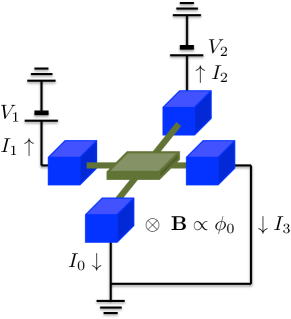
We are considering a 4-terminal Josephson junction, the setup of which is shown in Fig. 1. The superconducting leads are labeled by . The superconducting gap is assumed to be the same for all leads. Their phases are given by , where gauge invariance allows us to put . The leads are connected through a short normal region characterized by an energy-independent (unitary) scattering matrix for electrons. We further assume spin-rotation as well as time-reversal symmetry in the normal region, such that is spin-independent and . Thus belongs to the circular orthogonal ensemble (COE). We further restrict to junctions having one transmitting channel per terminal, such that is a matrix.
The spectrum of ABS with energy () in the junction is obtained by solving the eigenproblemBeenakker1991
| (1a) | |||
| (1b) | |||
Here, and are electron and hole outgoing wavefunctions from the normal region to lead , respectively, and is the Andreev reflection amplitude. Then, for each set of phases, Eq. (1) admits for four solutions at energies and (with ), which are pairwise opposite due to the built-in particle-hole symmetry in the theory of superconductivity.
According to Ref. Riwar2016, , scattering matrices drawn out of the COE can admit for zero-energy Weyl points in the ABS spectrum. These Weyl points correspond to topologically protected crossings of the two solutions with energies in the -space of superconducting phases. Each crossing is characterized by a topological charge , where
| (2) |
Here, is a surface in the -space that encloses the Weyl point, is an element of that surface, and
| (3) |
where is the Berry curvature associated with a normalized eigenstate with energy (with ). Time-reversal symmetry, together with the fermion-doubling theorem,Nielsen1981 imposes that the Weyl points appear in groups of four: there are two Weyl points of a given charge at , as well as two Weyl points of the opposite charge at . For definiteness, we chose . For phases , the Andreev spectrum is gapped in the entire -plane.
Subsequently, we define a (topological) Chern number in the -plane,
| (4) |
At , the setup is effectively a three-terminal junction, which does not admit for topologically protected crossings.Riwar2016 Time-reversal symmetry imposes that the Chern number . Increasing the phase , the Chern number changes when crossing by the charge of the corresponding Weyl point. Thus, we deduce that in the regions and , while it takes a value or in the intermediate region . Furthermore, .
According to adiabatic perturbation theory Riwar2016 , the Chern number determines the transconductance between two-voltage-biased terminals 1 and 2, , at sufficiently low voltage biases. To probe the transconductance quantization beyond the adiabatic regime, we will perform a numerical calculation of the current at arbitrary voltages for two specific setups (cf. Sec. III and Appendix). Below we motivate our choice for the two different scattering matrices describing these setups.
II.2 Examples
To obtain systems with Weyl points, we generate random symmetric scattering matrices within COE. This is done by first generating random hermitian matrices from the Gaussian unitary ensemble, and then forming , where is the unitary matrix that diagonalizes , i.e., with a real diagonal matrix. Around 5% of these matrices admit for Weyl points.
To observe the topological quantization of the transconductance, it is favorable to have a large gap in the Andreev spectrum between the Weyl points. Thus, for each scattering matrix with Weyl points, we determine the largest possible gap in the -plane for all in between the Weyl points,
| (5) |
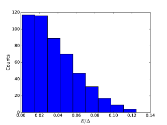
Furthermore, we do the same for all the remaining in the intervals and . A histogram of the smallest of these maximal gaps for an ensemble of topological scattering matrices is shown in Appendix A. We do not find any gap larger than around . For our simulation, we choose a topological scattering matrix with a gap close to that value.
Specifically, we use the matrix
| (6) |
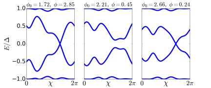
which has four Weyl points at , with charge , and , with charge . Taking as a control parameter, its maximal gap in the -plane for in between the two Weyl points is and is realized at . See Fig. 2 for some examples of the ABS spectrum of the four-terminal setup.
In the Appendix, we show results for a second scattering matrix, which has a smaller gap in between its Weyl points.
III Current-voltage characteristics
In this section we use the Landauer-Büttiker scattering formalism extended to superconducting hybrid structures to calculate the currents flowing through the setup at arbitrary voltage biases.Averin1995 We compare the numerical results with the prediction of the transconductance quantization at sufficiently low voltages.
III.1 Formalism
To obtain the transconductances and , we need to voltage bias leads 1 and 2. We will consider that they are voltage biased with commensurate voltages and ( integers), while . The d.c. currents flowing to the leads also depend on the phase bias , as well as on a phase shift between the time-dependent phases, and (with ). They are given by (below we set , unless they are explicitly written out)
| (7) |
where is the normal-state current, is the temperature, , and . Here generalizes the Andreev reflection amplitude to energies below and above the gap. It includes a phenomenological broadening parameter , also known as Dynes parameter (see below).dynes The outgoing electron and hole wavefunctions in lead associated with an incoming electron-like state from lead and with energy are given by the set of equations
| (8a) | |||||
| (8b) | |||||
which take into account inelastic scattering processes due to voltage biases. Here , , and .
The Dynes parameter generates a finite density of states at all energies below , , where is the density of states in the normal state. In particular, at . Thus it admits for inelastic relaxation of subgap states within the junction by coupling them with the small density of states in the leads. By contrast, when , quasiparticles can only relax their energy after performing successive Andreev reflections in the subgap region until they reach .
Note that topological conductance quantization has been predicted for incommensurate voltages.Riwar2016 As we work with commensurate voltages, the currents contain a Josephson-like contribution that depends periodically on the phase shift between the voltage-biased leads. This contribution has a small amplitude for commensurability ratios different from 1 (see Fig. 8 in the Appendix) and would vanish for incommensurate voltage biases. To extract the -independent part of the currents, we perform an average of the currents (7) over the phase shift .
The solution of the coupled equations (8) is implemented numerically as a matrix equation problem, making use of python’s scipy.linalg library (the solve_banded algorithm for solving a matrix equation with a sparse banded matrix). From the obtained wavefunctions, the currents are computed by the integration over energy in Eq. (7). For the integration we use direct summation over energies , with a sampling distance d. The computation time scales as . At voltage and fixed , computing all the currents for a single phase shift takes around 4h on a single CPU. Although the time can be reduced by parallelizing the integration over energy in Eq. (7), and the averaging over phase shifts (in practice, 10 equidistant phase shifts were sufficient to perform that average), this still limits the voltage range that we are able to efficiently probe.
In the next subsection, we show the numerical results for the scattering matrix , Eq. (6). Results for a different scattering matrix are shown in the Appendix.
III.2 Results
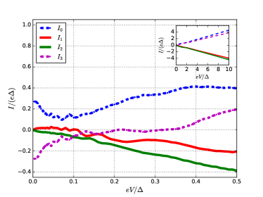
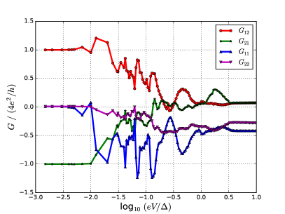
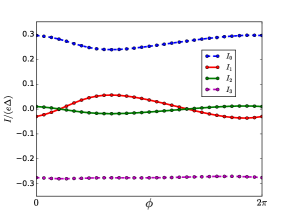
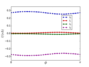
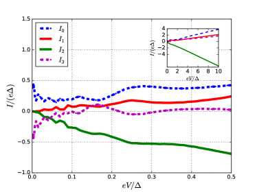
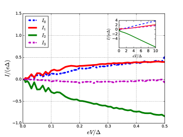
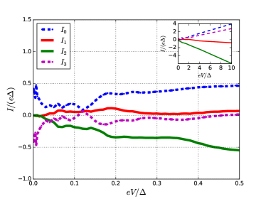
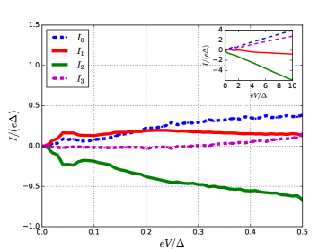
In Fig. 3 we show the curves for the 4-terminal setup with scattering matrix and a Dynes parameter . To extract the transconductances, we use two sets of values . Shown in the figure are the curves using and two different values of the phase bias . Note that the currents and have to tend to zero as voltage tends to zero. By contrast, a Josephson current may circulate in the ring between leads and at non-zero . This is seen in the top panel of Fig. 3, where tends to as the voltage tends to zero.
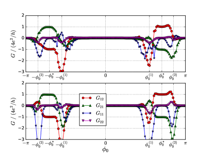
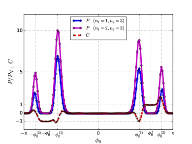
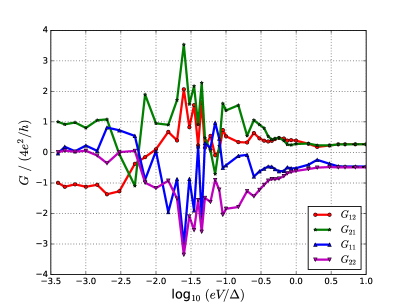
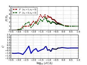
From the computed currents for the two sets of voltage biases, we obtain the conductance matrix , defined as , for (trivial region) and (topological region). Its elements as a function of voltage are shown in Fig. 4. At very low voltages, the direct conductances vanish, while the transconductances become quantized, . We now fix the voltage to a value small enough to observe conductance quantization and vary the control parameter . In Fig. 5, the dependence of the transconductance as a function of is shown for two different voltages. We see that the transconductance quantization holds for not too close to the values , where the topological transitions take place.
To help interpreting the results, we compute the dissipation of the system as a function of voltage, defined as . Using the two sets of voltages, we also compute the chirality, defined as
| (9) |
when . Here the primed variables are computed using the set and the unprimed using . The chirality selects the antisymmetric part of the conductance matrix. In a linear response regime, it reduces to . In particular, in the presence of time-reversal symmetry, it vanishes in the normal state. In Fig. 6, we plot the chirality as a function of voltage for the same structure as in Figs. 3-4, together with the normalized dissipation , where is the normal-state dissipation.
IV Discussion
The adiabatic perturbation theory that was used in Ref. Riwar2016, to predict the transconductance quantization requires the Andreev levels to retain their equilibrium occupations. In that regime, direct conductances vanish. On the other hand, multiple Andreev reflections allow for quasiparticle transfer between the leads by overcoming the energy gap . Thus, they result in charge transport at subgap voltages. At low voltages, these multiple Andreev reflections can be related with non-adiabatic transitions of quasiparticles occupying different branches of the Andreev spectrum as the phases increase linearly with time due to the voltage biases. Therefore the two regimes described above are competing. We expect that the transconductance quantization holds provided that an inelastic scattering process restores equilibrium occupation of the subgap states while suppressing multiple Andreev reflections. The Dynes parameter provides such a mechanism, while essentially preserving the superconducting gap if .
In Fig. 4 showing the conductance as a function of voltage, we can distinguish four different voltage regimes.
We see that, for high voltages , the conductance matrix elements match their normal-state values, . (Note that and due to the chosen conventions for the current directions.) In particular, , , and , corresponding to (cf. Figs. 4 and 6).
At lower voltages, , we observe a complex dependence of the direct conductances as well as the transconductances, with resonant features that are related with multiple Andreev reflections involving various leads.cuevas-pothier ; samuelsson-houzet ; quartets1 ; quartets2 ; physica ; quartets3
At even lower voltages, , the interplay between Landau-Zener transitions and inelastic relaxation becomes important. If is larger than the Landau-Zener transition rate between the states with energy and , it restores the equilibrium occupations, where the state with energy is occupied and the state with is empty, throughout most of the time evolution.
Thus, at very low voltages, , the direct conductances vanish, while the transconductances become quantized, . Namely, for (trivial region), and, for (topological region), .
The Landau-Zener transition rate at an avoided crossing between the two states is given as with . Here and for having an avoided crossing at . From the central panel of Fig. 2, which shows the cut in the plane of phases going through the minimal gap, we extract and for the scattering matrix . Using these values, our estimate for the Landau-Zener transition rate becomes at , which is in good agreement with the voltage where one starts to see low dissipation and the quantization of the transconductance (cf. Figs. 4 and 6).
When approaching the Weyl points, the gap in the -plane decreases. Thus, the voltage below which conductance quantization can be observed decreases as well. As shown in Fig. 5, at fixed voltage, we see a peak in the direct conductances around the Weyl points signaling that dissipation is large (see also Fig. 9 in Appendix B). The smaller the voltage, the more one can approach the Weyl points without losing the transconductance quantization.
V Conclusion
It has recently been predicted that multiterminal Josephson junctions may realize a novel type of topological matter.Riwar2016 Namely, for terminals, Weyl singularities may appear in the Andreev bound state spectrum of the junction, giving rise to topological transitions as the superconducting phases are tuned. These transitions are observable as quantized jumps in the transconductance between two voltage-biased terminals. In this work, we have studied this effect by numerically solving the Landauer-Büttiker scattering theory for a 4-terminal Josephson junction, which describes the quasiparticle transfer between the leads by the process of multiple Andreev reflection in the subgap regime. We have observed how the transconductances approach the quantized values predicted by the topology at low voltages, when dissipation is small. Tuning the superconducting phase at a fixed voltage, the topological transitions could be clearly seen. Our results provide an important step towards the clarification of the experimental conditions to observe the topological properties of multiterminal Josephson junctions.
Acknowledgements.
This work was supported by ANR, through grant ANR-12-BS04-0016-03, and by the Nanosciences Foundation in Grenoble, in the frame of its Chair of Excellence program.Appendix A Statistics of the largest possible spectral gaps for random scattering matrices with Weyl points
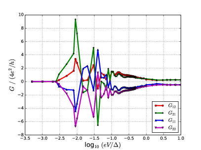
In order to find suitable scattering matrices for our numerical investigation, we analyzed an ensemble of random scattering matrices. In particular, we searched for the largest possible gap in the -plane, both in the topologically trivial and the topologically non-trivial regime. A histogram of the smaller of these maximal gaps in the two regions for an ensemble of topological scattering matrices is shown in Fig. 7. For our simulation, we choose two different topological scattering matrices: matrix , for which results are presented in the main text, with a gap close to the largest value we could obtain and matrix , for which results are presented in Appendix C, with a more typical gap.
Appendix B Additional results for the scattering matrix
To obtain the results presented in the main part, we averaged the currents over the phase offset between the phases of the leads 1 and 2. As shown in Fig. 8, the dependence of the currents on is weak and smooth, justifying this procedure.
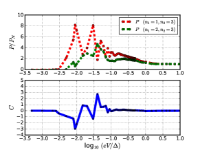
To observe the quantization of the transconductance, transport has to be quasi-adiabatic, i.e., dissipation has to be low. Close to the Weyl points, the gap around the Fermi level becomes very small and this breaks down. The dissipation as a function of the control parameter is shown in Fig. 9. Large peaks at the positions of the Weyl points are clearly visible. We also show the chirality that is expected to be zero in the trivial region and in the topological region. Due to the large dissipation, it deviates from these values in the vicinity of the Weyl points.
Appendix C Scattering matrix
The results presented in the main text were obtained for a scattering matrix that yields a particularly large gap in the topological region. As can be seen from Fig. 7, typical scattering matrices yield a smaller gap. In this section we make use of a second scattering matrix that is more typical,
| (10) |
Here the Weyl points are at , with charge , and , with charge . The gap in the topological region is largest in the planes at , where .
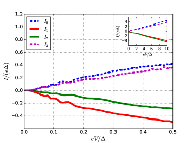
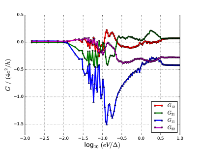
Due to the smaller gap, lower voltages have to be used to observe the quantization of the transconductance, making the calculations much more time-consuming. The current-voltage characteristics are shown in Fig. 10. The conductances are shown in Fig. 11. As explained in the main text, four different voltage regimes can be distinguished. At high voltages, , one find the normal state conductances, , , and . Lowering the voltage, , multiple Andreev reflections lead to resonance features. At even lower voltages, , the interplay between Landau-Zener transitions and inelastic relaxation becomes important. Here we chose a Dynes parameter . At , it becomes comparable to the Landau-Zener rate at voltage . This is consistent with the observed quantization at . The dissipation and the chirality are shown in Fig. 12.
References
- (1) M. Hasan and C. Kane, Rev. Mod. Phys. 82, 3045 (2010).
- (2) X.-L. Qi and S.-C. Zhang, Rev. Mod. Phys. 83, 1057 (2011).
- (3) C. Herring, Phys. Rev. 52, 365(1937).
- (4) S.Y. Xu et al., Science 349, 613 (2015).
- (5) B.Q. Lv et al., Phys. Rev. X 5, 031013 (2015).
- (6) L. Lu, Z. Wang, D. Ye, L. Ran, L. Fu, J. D. Joannopoulos, and M. Soljačić, Science 349, 622 (2015).
- (7) D.J. Thouless, M. Kohmoto, M. P. Nightingale, and M. den Nijs, Phys. Rev. Lett. 49, 405 (1982).
- (8) See, e.g., B.A. Bernevig, Topological Insulators and Topological Superconductors (Princeton University Press, Princeton, 2013).
- (9) A.Y. Kitaev, Phys. Usp. 44, 131 (2001).
- (10) L. Fu and C.L. Kane, Phys. Rev. B 79, 161408(R) (2009).
- (11) L.P. Rokhinson et al., Nature Physics 8, 795 (2012).
- (12) D.M. Badiane, L.I. Glazman, M. Houzet, and J.S. Meyer, C.R. Physique 14, 840 (2013).
- (13) R.S. Deacon et al., preprint arXiv:1603.09611.
- (14) F. Zhang and C.L. Kane, Phys. Rev. B 90, 020501 (2014).
- (15) B. van Heck, S. Mi, and A. R. Akhmerov, Phys. Rev. B 90, 155450 (2014).
- (16) C. Padurariu, T. Jonckheere, J. Rech, R. Mélin, D. Feinberg, T. Martin, and Yu. V. Nazarov, Phys. Rev. B 92, 205409 (2015).
- (17) R.-P. Riwar, M. Houzet, J. S. Meyer and Y.V. Nazarov, Nature Commun. 7, 11167 (2016).
- (18) T. Yokoyama and Y.V. Nazarov, Phys. Rev. B 92, 155437 (2015).
- (19) E. Strambini, S. D’Ambrosio, F. Vischi, F.S. Bergeret, Yu.V. Nazarov, and F. Giazotto, Nature Nanotechnology 11, 1055 (2016).
- (20) T. Yokoyama, J. Reutlinger, W. Belzig, and Y.V. Nazarov, preprint arXiv:1609.05455.
- (21) T.M. Klapwijk, G.E. Blonder, and M. Tinkham, Physica B & C 109-110, 1657 (1982).
- (22) D. Averin and A. Bardas, Phys. Rev. Lett. 75, 1831 (1995).
- (23) E.N. Bratus, V.S. Shumeiko, and G. Wendin, Phys. Rev. Lett. 74, 2110 (1995).
- (24) J.C. Cuevas, A. Martín-Rodero, and A.L. Yeyati, Phys. Rev. B 54, 7366 (1996).
- (25) C.W.J. Beenakker, Phys. Rev. Lett. 67, 3836 (1991).
- (26) H.B. Nielsen and M. Ninomiya, Nuclear Physics B 185, 20 (1981).
- (27) R.C. Dynes, V. Narayanamurti, and J.P. Garno, Phys. Rev. Lett. 41, 1509 (1978).
- (28) J.C. Cuevas and H. Pothier, Phys. Rev. B 75, 174513, (2007).
- (29) M. Houzet and P. Samuelsson, Phys. Rev. B 82, 060517(R) (2010).
- (30) T. Jonckheere, J. Rech, T. Martin, B. Douçot, D. Feinberg, and R. Mélin, Phys. Rev. B 87, 214501 (2013).
- (31) A.H. Pfeffer, J.E. Duvauchelle, H. Courtois, R. Mélin, D. Feinberg, and F. Lefloch, Phys. Rev. B 90, 075401 (2014).
- (32) R.-P. Riwar, D.M. Badiane, M. Houzet, J.S. Meyer and Y.V. Nazarov, Physica E 76, 231 (2016).
- (33) Y. Cohen, Y. Ronen, J.-H. Kang, M. Heiblum, D. Feinberg, R. Mélin, and H. Shtrikman, preprint arXiv:1606.08436.