Atomic-scale visualization of quasiparticle interference on a type-II Weyl semimetal surface
Abstract
We combine quasiparticle interference simulation (theory) and atomic resolution scanning tunneling spectro-microscopy (experiment) to visualize the interference patterns on a type-II Weyl semimetal MoxW1-xTe2 for the first time. Our simulation based on first-principles band topology theoretically reveals the surface electron scattering behavior. We identify the topological Fermi arc states and reveal the scattering properties of the surface states in Mo0.66W0.34Te2. In addition, our result reveals an experimental signature of the topology via the interconnectivity of bulk and surface states, which is essential for understanding the unusual nature of this material.
Recent discovery of type-I Weyl fermions in the TaAs class of materials has generated a flurry of new research directions Weyl1 ; Weyl2 ; Weyl3 ; Weyl4 ; Weyl5 ; rev1 ; rev2 ; TaAs1 ; TaAs2 ; ARPES-TaAs1 ; ARPES-TaAs2 . Many important predictions including Weyl cone, Fermi arc, chiral anomaly effect, and novel quasiparticle interference (QPI) were experimentally observed ARPES-TaAs1 ; ARPES-TaAs2 ; CA1 ; CA2 ; STM-NbP ; STM-TaAs1 ; STM-TaAs2 ; STM-TaAs3 . Very recently, a new type of Weyl quasiparticle was predicted in WTe2, MoTe2 and their alloys WTe2 ; MoTe1 ; MoTe2 ; MoTe3 . The novelty is that this type (type-II) of Weyl fermions breaks Lorentz symmetry, and thus can not exist as a fundamental particle in nature. Such an excitation can emerge in a crystal as low-energy quasiparticles. Theory predicts that type-II Weyl semimetals host a number of unusual effects, e.g. a new type of chiral anomaly, unconventional anomalous Hall effect and interaction-induced emergent Lorentz invariant properties, which are not possible in type-I Weyl semimetals typeII1 ; typeII2 ; typeII3 . Thus the experimental investigation of the MoWTe-class of materials is desirable.
Scanning tunneling microscopy/spectroscopy (STM/S) is a vital tool for the investigation and illumination of various key properties of a topological matter STM1 ; STM2 ; STM3 ; STM4 ; STM5 . The Fermi arc surface state, which is the topological fingerprint of Weyl semimetals, is predicted to exhibit exotic interference behavior in tunneling spectroscopy and magneto-transport measurements arc1 ; arc2 ; QPI1 ; QPI2 . Another unique property of a Weyl semimetal is the topological connection. An electron in a Fermi arc surface state, when moves to (or is scattered to) the Weyl node, will sink into the bulk and travel to the opposite surface arc1 . These features are interesting in connection to their QPI.
We employed low temperature STM/S to investigate the QPI patterns in MoxW1-xTe2. The Fermi arc-derived quantum interference patterns are identified. We also performed comprehensive first-principle band structure calculations and QPI simulations on this material for the first time. Combination of our experimental and theoretical results reveals signatures of the predicted unique topological connection in this material.
Single-crystalline Mo0.66W0.34Te2 samples were grown by chemical vapor transport method. After being cleaved at 79 K, they were transferred in vacuo to STM (Unisoku) at 4.6 K. dI/dV signals were acquired through a lock-in technique with a modulation at 5 mV and 1 kHz. Experimental QPI maps were generated by symmetrizing the Fourier transformed dI/dV maps (Fig. S1). First-principle based tight binding model simulations were used to obtain the electronic band structure. The alloy MoxW1-xTe2 was calculated by interpolation of the tight-binding model matrix elements of WTe2 and MoTe2. The theoretical QPI patterns are the restricted joint density of states, which removes all of the spin-flipping scattering vectors (see more details in the supplementary information).
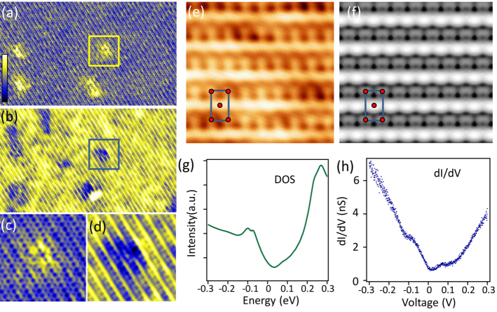
Figs. 1(a) and 1(b) present the typical morphology of the cleaved Mo0.66W0.34Te2(001) surface. There are only four point defects observed on the atomically ordered lattice, which confirms the high quality of our samples. In vicinity to the defect (Figs. 1 (c) and (d)), we observe a butterfly-like protrusion in the empty state image, and a depression area, which breaks the atomic row, in the occupied state. Since MoxW1-xTe2 is naturally cleaved at a Te-terminated surface, the point defect is attributed to a Te-vacancy. From the high resolution STM image of the occupied state (Fig. 1(e)), which probes the surface anions, we are able to clearly resolve an array of alternating atomic rows of extended (bright) and localized (dimmer) wave functions.The measured lattice constants (a=0.35 nm, b=0.63 nm) are consistent with the Te terminated Td phase of MoxW1-xTe2 lattice . The simulated STM image in Fig. 1(f) reproduces the surface structure of the alternating Te-atom rows. We also calculate the density of state, considering only the top Te layer. A typical dI/dV spectrum in Fig. 1(h) displays finite conductance at zero bias, which indicates the (semi-)metallic behavior of the samples. The measured data agrees qualitatively with the simulation, which confirms structural properties of our MoxW1-xTe2 sample, a candidate for the type-II Weyl semimetal.
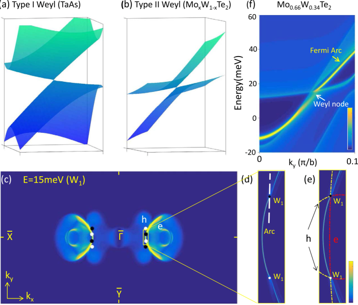
As shown in Fig. 2, the type-I Weyl cone consists of well separated upper and lower branches, and the constant energy contour (CEC) at the energy of Weyl node is a single point. By contrast, the type II cone is a heavily tilted in k-space, leading to the existence of projected bulk pockets (right and left branches of the Weyl cone) on the CEC at the Weyl node energy (and in a large energy range). MoxW1-xTe2 is predicted to be a type-II Weyl semimetal MoTe2 . Here, we focus on a x=0.66 sample. We uncover eight Weyl nodes in total. Four are located at 15 meV above the Fermi level (W1), while the other four nodes sit at 62 meV (W2). On the CEC at 15 meV (Fig. 2(c)), we find a typical type-II Weyl semimetal feature, the coexistence of projected bulk states and surface states. According to the penetration depth (see more details in Fig. S2), we are able to identify the two bright yellow semi-circular contours in Fig. 2 (c) as surface states and the remaining light-blue pockets (one bowtie-shaped hole pocket and two elliptical electron pockets) in Fig. 2 (c) as projected bulk states. We enlarge the surface state in the vicinity of the two W1 nodes in Figs. 2(d) and S2, and find that the surface band contour is split into three segments with tiny gaps in between. The middle segment behaves as a single curve connecting one pair of W1 nodes and is therefore identified as the Fermi arc. In Fig. 2 (e), we plot the edges of the projected bulk bands (the branches of the type-II Weyl cone), and clearly demonstrate they touch each other at the Weyl nodes. In addition, from the energy-momentum dispersion in Fig. 2(f), one can see the tilted cone in the band structure. Taking these evidences together, we theoretically establish the type-II Weyl state in our Mo0.66W0.34Te2 compound.
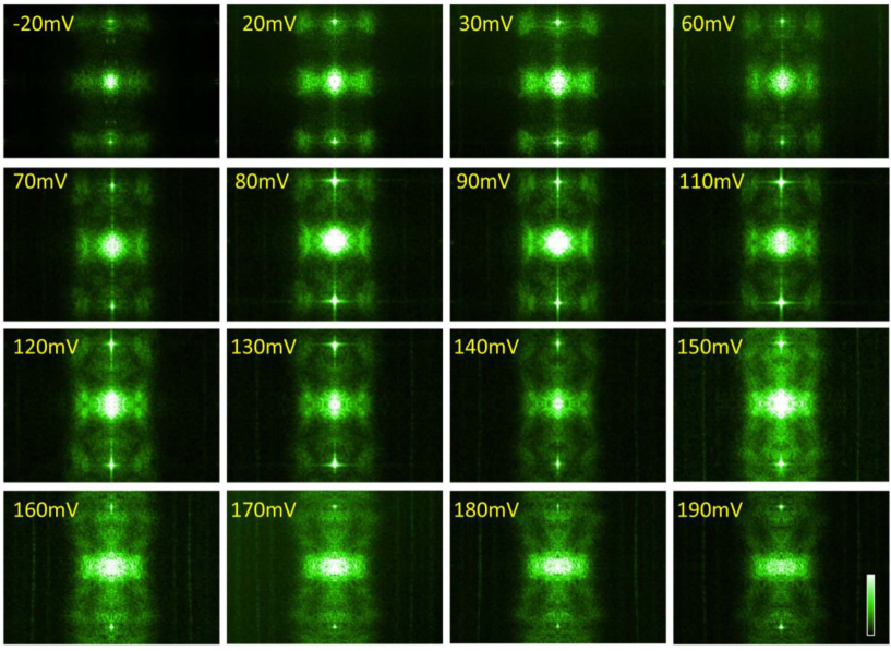
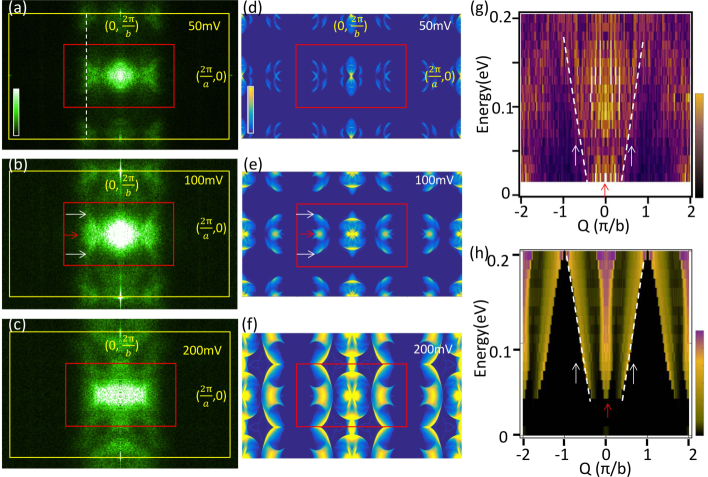
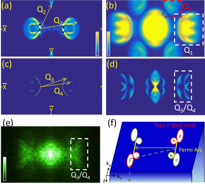
We perform dI/dV mapping on the Mo0.66W0.34Te2(001) surface at various voltages and Fourier transform these maps to gain insight of the QPI information in Figure 3. Figs. 4(a)-(c) exhibit the experimental QPI maps acquired at 50 meV, 100 meV and 200 meV above Fermi level. The patterns in the red rectangles arise from the intra-first BZ quasiparticle scatterings, while patterns close to the Bragg points (Qx,Qy)=(0,) with weaker intensities arise from the inter-BZ scattering and are replicas of the central features (Fig. S4). For simplicity, we restrict our discussion to the intra-BZ scattering (inside the rectangles) in the rest of this paper. At all energies (Fig. 3), the experimental QPIs show simple and clean patterns, in contrast to TaAs STM-NbP ; STM-TaAs1 ; STM-TaAs2 ; STM-TaAs3 . Specifically, all images consist of only three main pockets: one elliptical pocket in the center and two crescent-shaped contours located on the left and right sides of the central ellipse. The diameters of the crescents increase with bias voltage, which proves the electron like (instead of hole like) surface state. We perform model calculations to obtain the theoretical QPI patterns. Figs. 4(d)-(f) produce exactly the same number (three) of QPI pockets at the same locations in Q-space, and thus agree well with the experiments. Additionally, the calculated QPI at 100 meV (Fig. 4(e)) remarkably reproduces all dominant features in the measurement (Fig. 4(b)), namely, the central ellipse and the two side crescents. Moreover, the crescent displays a “3”-shape rather than a “” shape, the weak central feature as marked by the red arrow is also reproduced in the simulation in Fig. 4(e). To further examine the evolution of the QPI features, we study the energy-scattering vector (E-Q) dispersion. In Fig. 4(g) the data in the region between - and corresponds to the intra-BZ scattering. In this region, the QPI signal displays as a V-shaped dispersion, with the vertex of the V located at Q=0. The linear edges of the V-feature marked by white arrows refer to the two cutting points on the crescent pocket, which are indicated by white arrows in Fig. 4(b). Besides this strongly dispersed QPI feature, we also reveal an additional weakly dispersed feature, which is denoted by the red arrow and corresponds to the pocket indicated by the red arrow in Fig. 4(b). The calculated E-Q dispersion reproduces both features in the experimental data in a wide energy range.
Fig. 5 shows the QPI map at 50 meV, which is between the energies of W1 and W2. At this energy, the Fermi arcs give clear interference signals. In a type-II Weyl semimetal, the large projected bulk pockets always appear in the surface CEC. In the calculated “complete” CEC at 50 meV of the Mo0.66W0.34Te2(001) surface, which includes both bulk and surface states as shown in Fig. 5(a), we plot two dominant scattering vectors, namely connecting two electron pockets of the projected Weyl cone, and connecting the Weyl electron branch and the topologically trivial pocket at the points. In the simulated QPI pattern (Fig. 5(b)), one can clearly distinguish the - and -induced features. But the simulated QPI map consists of seven pockets, more than what was observed in experiment (three pockets). Hence, it can not be a correct interpenetration of our observation. However, the situation is improved by removing the bulk bands and taking only the surface states into account (Fig. 5 (c)). The surface CEC is comprised only of two large semicircular-shaped contours and four small arc-like pockets. The dominant scattering vectors are , which represents the scattering between two Fermi arc derived surface contours, and , which links the topological surface state to the trivial state. Both scattering processes involve the electrons in the Fermi arc. Therefore, the - and -derived QPI features inside the white rectangles in Fig. 5(d) serve as an explicit evidence of the QPI signal from Fermi arcs. In the QPI data in Fig. 5(e), we indeed observe these features. More importantly, the white rectangles in Figs. 4(d) and 4(e) are located in same positions and are the same size. This proves that we have observed QPI pockets with comparable dimensions appearing at the predicted locations, providing more solid evidence of the detection of Fermi arc in our experiment. The subtle differences in the fine QPI features may originate from the commonly used simple assumptions in the calculation ref . We emphasize that because MoxW1-xTe2 has a simple band structure, the major feature of the surface-state-derived QPI pattern is robust. In addition, the agreement between our theory and experiment is remarkably good compared to previous QPI results on other materials.
Furthermore, comparison of the two simulations in Figs. 5(b) and (d) to the experimental data (Fig. 5(e)) suggests that the contribution of the bulk states to the QPI signal is negligible. This can be attributed to the difficulty of establishing an interference between a three-dimensional bulk electronic wave and a two-dimensional surface wave. In other words, when a surface electron, which initially occupies a state in the Fermi arc, is scattered by a point defect into a bulk state, it loses its surface character and diffuses into the bulk. In this sense, the bulk Weyl pocket behaves like a sink of surface electrons, which is a signature of the topological connection between a Weyl cone and Fermi arc arc1 ; STM-TaAs1 ; STM-TaAs2 . On a type-I Weyl semimetal, the CEC at the energy of Weyl point consists of a point like bulk state, therefore the sinking effect is not prominent. By contrast, the type-II Weyl cones are heavily tilted, which gives rise to large areas of projected bulk pockets, and thus, this phenomenon should be more pronounced on a type-II Weyl semimetal surface.
In summary, we present theoretical QPI simulations and STM results on MoxW1-xTe2 illustrating its complex electronic structure for the first time, which are complementary to the recent ARPES measurements MoTe2-ARPES1 ; MoTe2-ARPES2 . Our QPI measurements directly discern the topological Fermi arcs. Taken together, our calculations and experiment data suggest that the interference pattern is dominated by surface states, whereas the contribution from bulk states to QPI is negligible, indicating the topological connection between the Weyl bulk states and Fermi arc surface states. Our results on MoxW1-xTe2 establish a platform for further study of novel spectroscopic, optical, and transport phenomena that emerge in this compound.
After the completion of this theoretical plus experimental STM paper, we became aware of partial experimental STM data in a concomitant mainly-ARPES paper MoTe2-ARPES3 .
H.Z., G.B., S.-Y.X., I.B., N.A., D.S.S., S.Z. and M.Z.H. are supported by the Gordon and Betty Moore Foundations EPiQS Initiative through Grant GBMF4547 and U.S. National Science Foundation (NSF) Grant No. NSFDMR-1006492. H.Z also thanks the support from National Natural Science Foundation of China (No.11674226). G.C., and H.L. thank the National Research Foundation, Prime Ministers Office, Singapore, under its NRF fellowship (NRF Award No. NRF-NRFF2013-03). H.L., G.W., and S.J. are supported by National Basic Research Program of China (Grant No. 2013CB921901 and 2014CB239302). N.Y. is supported in part by funding from the Princeton Center for Complex Materials, a MRSEC supported by NSF Grant DMR 1420541. T.-R.C. and H.-T.J. are supported by Ministry of Science and Technology, Academia Sinica, and National Tsing Hus University, Taiwan, and also thank NCHC, CINC-NTU, and NCTS, Taiwan, for technical support. F.S. acknowledge the National Key Projects for Basic Research of China (No:2013CB922103) and the National Natural Science Foundation of China (Grant Nos: 91421109, 11134005, 11522432). A.B. is supported by the US Department of Energy (DOE), Office of Science, Basic Energy Sciences Grant No. DE-FG02-07ER46352, and benefited from Northeastern University’s Advanced Scientific Computation Center (ASCC) and the NERSC supercomputing center through DOE Grant No. DE-AC02-05CH11231.
References
- (1) S. Murakami, New. J. Phys. 9, 356 (2007).
- (2) X. Wan, A. M. Turner, A. Vishwanath, and S. Y. Savrasov, Phys. Rev. B 83, 205101 (2011).
- (3) L. Balents, Physics 4, 36 (2011).
- (4) A. A. Burkov, and L. Balents, Phys. Rev. Lett. 107, 127205 (2011).
- (5) T. Ojanen, Phys. Rev. B 87, 245112 (2013).
- (6) M. Z. Hasan, S.-Y. Xu, and G. Bian, Phys. Scr. T164, 014001 (2015).
- (7) A. M. Turner, and A. Vishwanath, arXiv:1301.0330.
- (8) S.-M. Huang, S.-Y. Xu, I. Belopolski, C.-C. Lee, G. Chang, B. Wang, N. Alidoust, G. Bian, M. Neupane, C. Zhang, S. Jia, A. Bansil, H. Lin, and M. Z. Hasan, Nature Commun. 6, 7373 (2015).
- (9) H. Weng, C. Fang, Z. Fang, B. A. Bernevig, and X. Dai, Phys. Rev. X 5, 011029 (2015).
- (10) S.-Y. Xu, I. Belopolski, N. Alidoust, M. Neupane, G. Bian, C. Zhang, R. Sankar, G. Chang, Z. Yuan, C.-C. Lee, S.-M. Huang, H. Zheng, J. Ma, D. S. Sanchez, B. Wang, A. Bansil, F. Chou, P. P. Shibayev, H. Lin S. Jia, and M. Z. Hasan, Science 349, 613 (2015).
- (11) B. Q. Lv, H. M. Weng, B. B. Fu, X. P. Wang, H. Miao, J. Ma, P. Richard, X. C. Huang, L. X. Zhao, G. F. Chen, Z. Fang, X. Dai, T. Qian, and H. Ding, Phys. Rev. X 5, 031013 (2015).
- (12) X. Huang, L. Zhao, Y. Long, P. Wang, D. Chen, Z. Yang, H. Liang, M. Xue, H. Weng, Z. Fang, X. Dai, and G. Chen, Phys. Rev. X 5, 031023 (2015).
- (13) C.-L. Zhang, S.-Y. Xu, I. Belopolski, Z. Yuan, Z. Lin, B. Tong, G. Bian, N. Alidoust, C.-C. Lee, S.-M. Huang, T.-R. Chang, G. Chang, C.-H. Hsu, H.-T. Jeng, M. Neupane, D. S. Sanchez, H. Zheng, J. Wang, H. Lin, C. Zhang, H.-Z. Lu, S.-Q. Shen, T. Neupert, M. Z. Hasan and S. Jia, Nature Commun. 7, 10735 (2015).
- (14) H. Zheng, S.-Y. Xu, G. Bian, C. Guo, G. Chang, D. S. Sanchez, I. Belopolski, C.-C. Lee, S.-M. Huang, X. Zhang, R. Sankar, N. Alidoust, T.-R. Chang, F. Wu, T. Neupert, F. Chou, H.-T. Jeng, N. Yao, A. Bansil, S. Jia, H. Lin, and M. Z. Hasan, ACS Nano 10, 1378 (2016).
- (15) H. Inoue, A. Gyenis, Z. Wang, J. Li, S. W. Oh, S. Jiang, N. Ni, B. A. Bernevig, and A. Yazdani, Science 351, 1184 (2016).
- (16) R. Batabyal, N. Morali, N. Avraham, Y. Sun, M. Schmidt, C. Felser, A. Stern, B. Yan, and H. Beidenkopf, Sci. Adv. 2, e1600709 (2016)
- (17) P. Sessi, Y. Sun, T. Bathon, F. Glott, Z. Li, H. Chen, L. Guo, X. Chen, M. Schmidt, C. Felser, B. Yan, and M. Bode, arXiv:1606.00243.
- (18) A. A. Soluyanov, D. Gresch, Z. Wang, Q. Wu, M. Troyer, Xi Dai, and B. A. Bernevig, Nature 527, 495 (2015).
- (19) Y. Sun, S.-C Wu, M. N. Ali, C. Felser, and B. Yan, Phys. Rev. B 92, 161107 (2015).
- (20) T.-R. Chang, S.-Y. Xu, G. Chang, C.-C. Lee, S.-M. Huang, B. Wang, G. Bian, H. Zheng, D. S. Sanchez, I. Belopolski, N. Alidoust, M. Neupane, A. Bansil, H.-T. Jeng, H. Lin, and M. Z. Hasan, Nature Commun. 7, 10639 (2016).
- (21) Z. Wang, D. Gresch, A. A. Soluyanov, W. Xie, S. Kushwaha, X. Dai, M. Troyer, R. J. Cava, and B. A. Bernevig, Phys. Rev. Lett. 117, 056805 (2016).
- (22) A. G. Grushin, Phys. Rev. D 86, 045001 (2012).
- (23) A. A. Zyuzin, and R. P. Tiwari, JETP Lett. 103, 717 (2016)
- (24) H. Isobe, and N. Nagaosa, Phys. Rev. Lett. 116, 116803 (2016)
- (25) P. Roushan, J. Seo, C. V. Parker, Y. S. Hor, D. Hsieh, D. Qian, A. Richardella, M. Z. Hasan, R. J. Cava and A. Yazdani, Nature 460, 1106 (2009).
- (26) T. Zhang, P. Cheng, X. Chen, J.-F. Jia, X. Ma, K. He, L. Wang, H. Zhang, X. Dai, Z. Fang, X. Xie, and Q.-K. Xue, Phys. Rev. Lett. 103, 266803 (2009).
- (27) I. Lee, C. K. Kim, J. Lee, S. J. L. Billinge, R. Zhong, J. A. Schneeloch, T. Liu, T. Valla, J. M. Tranquada, G. Gu, and J. C. S. Davis, Proc. Natl. Acad. Sci. U.S.A. , 1316 (2015).
- (28) I. Zeljkovic, Y. Okada, C.-Y. Huang, R. Sankar, D. Walkup, W. Zhou, M. Serbyn, F. Chou, W.-F. Tsai, H. Lin, A. Bansil. L. Fu, M. Z. Hasan and V. Madhavan, Nat. Phys. , 572 (2014).
- (29) D. Zhang, H. Baek, J. Ha, T. Zhang, J. Wyrick, A. V. Davydov, Y. Kuk, and J. A. Stroscio, Phys. Rev. B 89, 245445 (2014).
- (30) A. C. Potter, I. Kimchi, and A. Vishwanath, Nature Commun. 5, 5161 (2014).
- (31) P. Hosur, Phys. Rev. B 86, 195102 (2012).
- (32) G. Chang, S.-Y. Xu, H. Zheng, C.-C. Lee, S.-M. Huang, I. Belopolski, D. S. Sanchez, G. Bian, N. Alidoust, T.-R. Chang, C.-H. Hsu, H.-T. Jeng, A. Bansil, H. Lin, and M. Z. Hasan, Phys. Rev. Lett. 116, 066601 (2016).
- (33) A. K. Mitchell, and L. Fritz, Phys. Rev. B 93, 035137 (2016).
- (34) B. Brown, Acta. Cryst. 20, 268 (1966).
- (35) To simulate a QPI pattern in Q-space, it is a common practice to calculate the joint density of states with restrictions from spin and/or orbital textures. The simulation is simplified by considering the point defect as a -function, by ignoring the shape of its wavefunction and scattering anisotropy of the defect. Though it may cause some minor discrepancy in the fine structures, it is widely accepted that the simulation is capable of capturing all dominated QPI features (the number, positions and sizes of QPI pockets).
- (36) I. Belopolski, S.-Y. Xu, Y. Ishida, X. Pan, P. Yu, D. S Sanchez, H.Zheng, M. Neupane, N. Alidoust, G. Chang, T.-R. Chang, Y. Wu, G. Bian, S.-M. Huang, C.-C. Lee, D. Mou, L. Huang, Y. Song, B. Wang, G. Wang, Y.-W. Yeh, N. Yao, J. E. Rault, P. Le Fevre, F. Bertran, H.-T. Jeng, T. Kondo, A. Kaminski, H. Lin, Z. Liu, F. Song, S. Shin, and M. Z. Hasan, Phys. Rev. B 94, 085127 (2016).
- (37) A. Tamai, Q. S. Wu, I. Cucchi, F. Y. Bruno, S. Ricco, T. K. Kim, M. Hoesch, C. Barreteau, E. Giannini, C. Besnard, A. A. Soluyanov, and F. Baumberger, Phys. Rev. X 6, 031021 (2016).
- (38) K. Deng, G. Wan, P. Deng, K. Zhang, S. Ding, E. Wang, M. Yan, H. Huang, H. Zhang, Z. Xu, J. Denlinger, A. Fedorov, H. Yang, W. Duan, H. Yao, Y. Wu, S. Fan, H. Zhang, X. Chen, and S. Zhou, Nat. Phys. online published.