Roughness-induced domain structure in perpendicular Co/Ni multilayers
Abstract
We investigate the correlation between roughness, remanence and coercivity in Co/Ni films grown on Cu seed layers of varying thickness. Increasing the Cu seed layer thickness of Ta/Cu/8x[Co/Ni] thin films increases the roughness of the films. In-plane magnetization loops show that both the remanence and coercivity increase with increasing seed layer roughness. Polar Kerr microscopy and magnetic force microscopy reveal that the domain density also increases with roughness. Finite element micromagnetic simulations performed on structures with periodically modulated surfaces provide further insight. They confirm the connection between domain density and roughness, and identify the microsocpic structure of the domain walls as the source of the increased remanence in rough films. The simulations predict that the character of the domain walls changes from Bloch-like in smooth films to Néel-like for rougher films.
1 Introduction
Modern magnetic devices are typically multilayer structures made of a combination of thin magnetic and non-magnetic films. Much current research focuses on films with perpendicular magnetic anisotropy (PMA) as they provide an avenue for creating devices that have higher storage density [1, 2] and lower switching currents [3] while maintaining thermal stability. Such films have been widely studied for use in perpendicular magnetic recording media [4, 5, 6, 7, 8], racetrack memory [9, 10], patterned magnetic media [11], and spin-transfer torque magnetic random access memory (STT-MRAM) devices [12]. Co/Ni multilayers are one of many PMA materials that have been proposed for these applications. Since their prediction and observation in 1992 by Daalderop et al. [13] they have come under intense scrutiny as they offer the possibility of low cost magnetic devices with large PMA.
Understanding the magnetic properties of thin films is complicated by the fact that they invariably suffer from some degree of roughness when grown under real-world conditions. It is well known that the roughness of magnetic thin films plays a large role in determining properties such as magnetic anisotropy [14, 15, 16], coercivity [15], domain structure, magnetization reversal process, and demagnetizing factor [14]. Magnetic anisotropy has been shown to increase when films are grown on smoother substrates [15] or on smoother seed (buffer) layers [16]. The increased coercivity observed in films grown on rougher substrates has been attributed to the pinning of domain walls [17]. In particular, defects at the interfaces have been cited as the reason for this extra pinning [15]. Despite the large amount of theoretical and experimental work, the effects of roughness are not yet fully understood. For example, there is a lack of micromagnetic modeling on rough films, which can provide insight into domain-wall structures that would otherwise be inaccessible to experimental techniques.
This study was undertaken to explore some of the effects that roughness has on the magnetization reversal of thin films with PMA in the presence of an in-plane magnetic field. We prepared PMA multilayers with well controlled roughness and have combined this experimental study with finite element micromagnetic simulations. Cross-sectional transmission electron microscopy (TEM) and atomic force microscopy (AFM) were used to study the roughness; polar magneto-optical Kerr effect (MOKE) microscopy and magnetic force microscopy (MFM) to investigate the magnetic domain structure; and SQUID/VSM to measure the magnetization loops. The finite element simulations confirm the experimentally observed changes in domain size with roughness, and provide further insight into the source of in-plane coercivity and remanence in thin films with PMA. In the following discussion we consider three types of films: completely flat; smooth (small roughness); and rough (large roughness).
2 Sample preparation
The films used in this study have composition
Ta(3)/Cu()/8[Co(0.21)/Ni(0.57)]/Ta(3), with thicknesses
given in nanometers. The Cu seed layer thickness was systematically increased
as this has been shown to increase surface roughness in a controlled
manner [17]. All layers were deposited at room
temperature on Si (001) wafers using both RF (Co, Ni, Ta) and DC (Cu)
magnetron sputtering at an argon pressure of torr. The base
pressure of the system was below torr. Before deposition the
substrates were cleaned with the RCA Standard Clean 1 (SC-1)
procedure [18] to remove organic contaminants. This
leaves a thin layer on the surface of the Si. The Ta and Cu seed
layers serve to establish growth along the directions, which
is required to obtain large PMA in Co/Ni. In this study, the Cu seed layer
thickness, , was varied from 2 to 30 nm. X-ray diffraction
measurements indicate that the Co/Ni multilayers grew along the
directions. The films are strongly textured with the full
width at half maximum of the (111) peak below in an X-ray rocking
curve measurement.
3 Results and Discussion
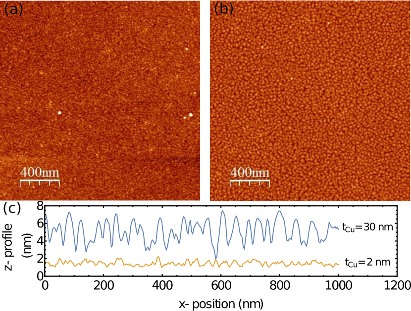
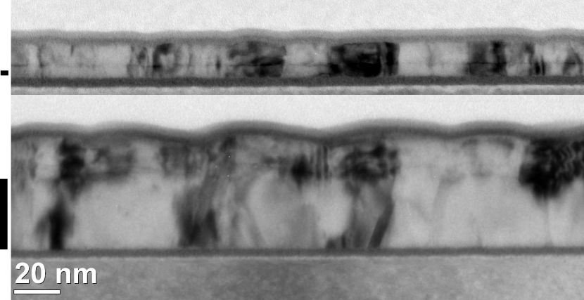
Figure 1 shows AFM images of Co/Ni multilayer films grown on 2 and 30 nm thick Cu seed layers, and corresponding topography profiles. The RMS roughness and grain size of the films increase with seed layer thickness, see Table 1.
In addition to the films prepared specifically for this study we have included TEM measurements from comparable Co/Ni multilayer stacks previously studied for STT-MRAM applications that were grown on seed layers that have the same thickness as the ones used in this study. Figure 2 shows that the Co/Ni films follow the morphology of the seed layer. The STT-MRAM films grown on thin Cu seed layers are almost smooth with a mean grain size of 20 nm and a mean grain height (trough to peak) of 1.6 nm. The films grown on thick Cu seed layers are rough and have a mean grain size of 40 nm with a mean variation in grain height of 4 nm. The modulation of the multilayer height is then similar to the thickness of the Co/Ni multilayer.
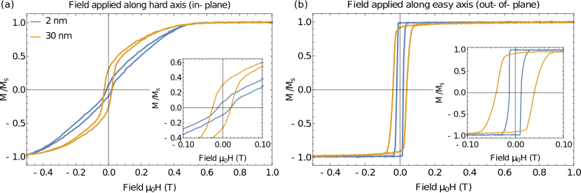
In-plane and out of plane hysteresis loops measured by vibrating sample magnetometry (VSM) for the nm and nm samples are shown in Figure 3. The in-plane coercivity and remanence for the rough film are more than twice as large as those of the smooth film, and there is substantial rounding of the hysteresis loop in the rough film. These effects are confirmed by more precise SQUID measurements, which are presented in Figure 5 (d,e). The coercivity measured perpendicular to the film is significantly larger for the rough film than for the smooth one, but the squareness of the hysteresis loop, , is only 0.92 for the rough film as opposed to approximately 1 for the smooth film.
| RMS Roughness | Grain size | |||||
|---|---|---|---|---|---|---|
| (nm) | (kA/m) | (kA/m) | ( J/m3) | (kA/m) | (nm) | (nm) |
| 2.0(1) | 649(13) | -337.4(2) | 4.00(5) | 7.0(4) | 0.25 | 25 |
| 12.0(3) | 655(13) | -354.4(2) | 4.15(5) | 21.5(8) | 0.73 | 37 |
| 30.0(9) | 675(13) | – | – | 1.17 | 43 |
The magnetic anisotropy of the Co/Ni films was measured using ferromagnetic resonance (FMR) in a terminated waveguide, in a field-swept, field-modulated configuration, as detailed by Montoya et al. [20] The FMR measurements were performed between 45 GHz and 69 GHz, with field applied both parallel and perpendicular to the film surface. In order to extract the uniaxial anisotropy, , we first fit the frequency dependence of the resonance and used
where is the effective demagnetization field and is the saturation magnetization, which was measured using a SQUID magnetometer in magnetic fields up to T. The results are shown in Table 1.
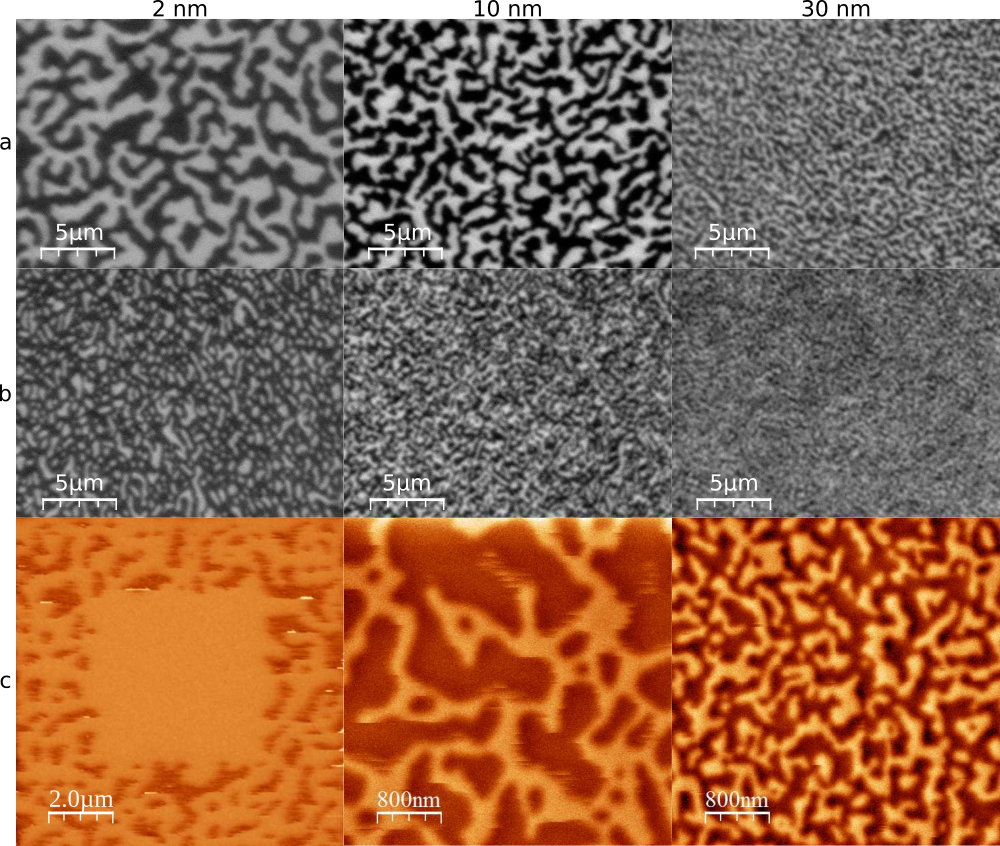
Figure 4 shows the magnetic domain structure of three different films as imaged by Kerr and magnetic force microscopy. The polar Kerr images (Figure 4 a) after ac-demagnetizing the samples in the out-of-plane direction show the patchy up/down domain pattern often observed in thin films with PMA, such as epitaxial L10 FePt or -axis oriented films [23]. The effect of roughness shows up as a substantial reduction in the size of the domains from about 1.2 m average domain size for the smoothest film ( nm) to about 400 nm for the roughest film ( nm). We will see later that similar effects appear in our micromagnetic simulations. Interestingly, also after in-plane saturation, i.e., after a field has been applied along the hard axis, the domain structure refines with increasing surface roughness (Figure 4 b). The average domain sizes are, however, much smaller (from 700 nm down to 300 nm) and become difficult to resolve by optical microscopy for the film prepared on the 30 nm thick Cu buffer. We thus resort to imaging the same sample state with magnetic force microscopy (MFM) in a Bruker Icon AFM/MFM with high resolution/low moment tips (225c07ML1) purchased from Team Nanotec. The choice of tips is motivated by the small out-of-plane coercivity of the samples, which is easily exceeded by the stray field of standard tips when in close proximity to the film surface. Indeed, imaging the smoothest sample failed even with the low moment tips. Figure 4 (c, 2nm) shows the MFM image of the smoothest sample after performing a first scan on a small area and then a second scan on a larger area; the domains were fully pushed/pulled out of the first scan area. This means that the domain structure seen in Figure 4 (c, 2nm) is not representative of the actual domains in the film. For the slightly rougher film ( nm) the MFM measurement still displays some ‘wiping’ features corresponding to the above mentioned issue, but the out-of-plane domain structure is already qualitatively visible. MFM performed on the roughest sample results in a clear image of the perpendicular domains and the small nm features are clearly resolved.
Finite element micromagnetic simulations have been used to obtain further insights into the magnetic structure of films with PMA in in-plane applied fields, in particular the increased domain density caused by roughness. The lateral dimensions of the simulated films are 1000 nm 1000 nm, and the film thickness is 6.24 nm to match that of the real films. To ensure that finite element discretization was not affecting the results, we quantified the smallest exchange lengths relevant to the simulations. Using definitions for the exchange lengths from Abo et al. [24] we took for the magnetostatic exchange length and for the magnetocrystalline exchange length. Here is the exchange interaction constant and is the uniaxial anisotropy constant. With the experimentally determined film properties and assuming a lower bound of J/m, this gives nm and nm. Since these values are somewhat less than the thickness of the magnetic layers in the actual sample, there is a concern that spurious effects due to discretization may influence the results. To place an upper bound on these effects, simulations were carried out for two different regimes of discretization: one in which the magnetic film is divided vertically into three layers, and one in which the film is treated as a single layer. No significant differences between the 3-layer and single-layer simulations are observed, giving us confidence in the discretization process. In particular, domain walls in the 3-layer simulations run perpendicular to the film surface, showing that the magnetic moments are coupled tightly together in this direction. With this consistency check in hand, the simulations in the remainder of the paper were carried out in the single-layer approximation, significantly reducing computation time.
Roughness has been simulated by imposing the following modulation onto the surface:
Note that this model is a simplification of the experimental situation, in which the grains have a distribution of heights and sizes — this level of the simulation is intended mainly to be illustrative of the effect of roughness. Detailed fits to experiment lie beyond the scope of the theory, and in any case would not be possible because the calculations are too computationally intensive to exhaustively explore parameter space.
The direction of uniaxial anisotropy is initially set parallel to the local film normal and then a distortion is applied to the anisotropy direction to simulate the effects of the grains not growing perfectly along the directions. The range of distortions in the following simulations was set to , meaning that the local anisotropy direction deviated from the surface normal by up to (with the angle chosen at random from a uniform distribution). The simulations started by saturating the sample in the direction in an external field of T. The external field was then reduced in steps to T. Each simulation was run 10 times with different random distributions of the easy axis, and the hysteresis loops in the figures are the average of the 10 runs.
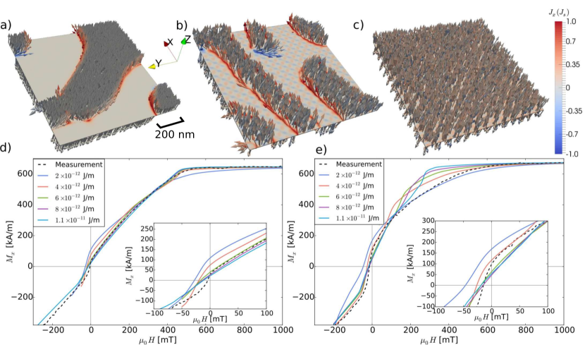
Two sets of simulations were initially performed, one of perfectly flat samples, the other of rough samples. The roughness parameters are nm and nm for the rough samples. All other parameters (, , ) are common. Typical domain structures for these films in zero applied field, following saturation in the + direction, are shown in Figure 5 (a,b). The rough films had a higher number of domains in all simulations, in agreement with the experimental observations.
The exchange interaction determines the domain-wall width, , and the domain-wall energy density, . The competition between domain-wall energy, which favours fewer domains, and dipole energy, which favours more domains, is therefore tied to the exchange interaction. This is indeed observed in the simulations: reducing the exchange coupling to J/m decreases the domain wall thickness, and is accompanied by a large increase in the number of domains, almost to the point that individual domains are indistinguishable, as shown in Figure 5 (c).
Simulations were then performed in order to understand the origin of the nonzero remanence. To do this, we varied between J/m and J/m, while setting and to their experimentally determined values (see Table 1). Figure 5 (d,e) show that substantial rounding of the magnetization curves is found in simulations with small exchange constant. The rounding of the rough film hysteresis loops therefore indicate that the exchange constant in rough films is lower than that of the smooth films. The reduction of the exchange constant in the rough film can be accounted for by the fact that the grains in the rough film have domed surfaces: this reduces the contact area between grains, resulting in a lower effective exchange interaction.
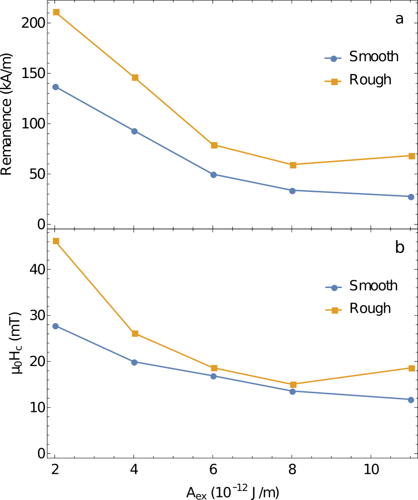
The larger in-plane coercivity found in the rough films is in part caused by the reduced intergranular coupling. Roughness, however, plays a much larger role than simply lowering . In Figure 6 we see that even for the same exchange constant both the in-plane remanence and in-plane coercivity of the rough films are larger than those of the smooth films. It is clear that the increased coercivity and remanence cannot be attributed to defects or impurities as the micromagnetic simulations do not include these effects. Roughness on its own is therefore enough to increase the coercivity and remanence.
A striking feature of all the simulations is that the magnetization in the domain walls points predominantly in the direction of the saturating magnetic field once the field is removed. This causes the nonzero remanence in these films and leads to a larger remanence in the rough film since roughness increases the number of domain walls. This observation is in accord with the magnetization data shown in Figure 3, where the rough film remanence is more than twice that of the smooth film. The simulations also show that the domain walls, which occupy only a small fraction of the total film volume, account for approximately 75% of the remanence, with the rest coming from within the domains. A study of 200 nm Ni grown on 50 nm Cu by Marioni et al. [25] came to the same conclusions: the large in-plane remanence is mostly due to the net magnetization of the domain walls.
In simulations of perfectly flat films the domain walls are always of Bloch type. This has the effect that only the component of the domain wall moments that runs parallel to the -axis (applied field direction) contributes to the remanence. Even in completely flat films, there is a preference for the domain wall moments to align along the direction, resulting in a nonzero remanence.
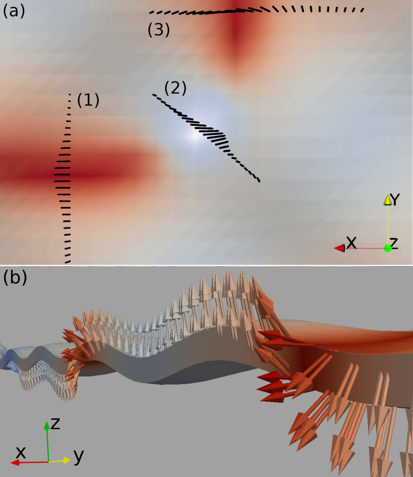
The situation in rough films is more complicated. In Figure 7 (a), domain wall 1 is aligned parallel to the applied field (-axis) and is of Bloch-wall type. Domain wall 3 is aligned perpendicular to the applied field, and is of Néel type. Domain wall 2, oriented at an intermediate angle, is of mixed Bloch-Néel character. In all three cases there is an -component of magnetization, suggesting that all domain walls contribute to the remanence.
A consequence of the moments in the domain walls aligning predominantly in the direction of the applied field in rough films is that the chirality of the domain walls reverses at either side of the domain – if it did not reverse then the film would have no remanence. An example of the reversing chirality is shown in Figure 7 (b). Because of the reversing chirality, neighbouring domain walls carry opposite topological charge. The domain walls can easily annhilate if brought close together, as opposed to the case in films with single chirality, where at low fields topological charge can only enter and leave the material at its boundaries [26, 27].
4 Conclusions
We have shown that roughness plays a crucial role in determining the in-plane magnetic properties of thin films with PMA. Roughness increases the in-plane remanence, coercivity, and domain density. Micromagnetic simulations link the increased remanence to the domain density; the moments within the domain walls point predominantly along the in-plane applied field direction, which, combined with an increased number of domain walls, results in the increased remanence. The simulations also predict that roughness can affect the energy balance between Néel and Bloch walls. In the smooth films considered here the domains are all Bloch-like, whereas in the rough films we also find Néel-like and mixed Bloch-Néel walls. Further experiments are needed to verify this effect.
Acknowledgments
The authors thank S. Pofahl for technical help with the Kerr microscope. Financial support by the Natural Sciences and Engineering Research Council of Canada, the Canadian Institute for Advanced Research, the Austrian Science Fund (FWF): I2214-N20, the Austrian Federal Ministry of Science, Research and Economy, and the National Foundation for Research, Technology and Development is gratefully acknowledged. Support from the structural characterization facilities at the HZDR Ion Beam Center is gratefully acknowledged.
References
- [1] Andreas Moser, Kentaro Takano, David T. Margulies, Manfred Albrecht, Yoshiaki Sonobe, Yoshihiro Ikeda, Shouheng Sun, and Eric E. Fullerton. Magnetic recording: advancing into the future. J. Phys. D: Appl. Phys., 35(19):R157, 2002.
- [2] S. N. Piramanayagam. Perpendicular recording media for hard disk drives. Journal of Applied Physics, 102(1):011301, July 2007.
- [3] S. Mangin, D. Ravelosona, J. A. Katine, M. J. Carey, B. D. Terris, and Eric E. Fullerton. Current-induced magnetization reversal in nanopillars with perpendicular anisotropy. Nat Mater, 5(3):210–215, March 2006.
- [4] Erol Girt, S. Wu, B. Lu, G. Ju, T. Nolan, S. Harkness, B. Valcu, A. Dobin, J. D. Risner, M. Munteanu, R. Thangaraj, C.-H. Chang, T. Tran, X. Wu, O. Mryasov, D. Weller, and S. Hwang. Influence of oxide on the structural and magnetic properties of CoPt alloy. Journal of Applied Physics, 99(8):08E715, April 2006.
- [5] H. J. Richter. The transition from longitudinal to perpendicular recording. J. Phys. D: Appl. Phys., 40(9):R149, 2007.
- [6] T. P. Nolan, J. D. Risner, S. D. Harkness, E. Girt, S. Z. Wu, G. Ju, and R. Sinclair. Microstructure and Exchange Coupling of Segregated Oxide Perpendicular Recording Media. IEEE Transactions on Magnetics, 43(2):639–644, February 2007.
- [7] E. Girt, A. Y. Dobin, B. Valcu, H. J. Richter, X. Wu, and T. P. Nolan. Experimental Evidence of Domain Wall Assisted Switching in Composite Media. IEEE Transactions on Magnetics, 43(6):2166–2168, June 2007.
- [8] V. Neu, C. Schulze, M. Faustini, J. Lee, D. Makarov, D. Suess, S.-K. Kim, D. Grosso, L. Schultz, and M. Albrecht. Probing the energy barriers and magnetization reversal processes of nanoperforated membrane based percolated media. Nanotechnology, 24(14):145702, 2013.
- [9] Stuart Parkin and See-Hun Yang. Memory on the racetrack. Nat Nano, 10(3):195–198, March 2015.
- [10] Stuart S. P. Parkin, Masamitsu Hayashi, and Luc Thomas. Magnetic Domain-Wall Racetrack Memory. Science, 320(5873):190–194, April 2008.
- [11] C. A. Ross. Patterned Magnetic Recording Media. Annual Review of Materials Research, 31(1):203–235, 2001.
- [12] A. V. Khvalkovskiy, D. Apalkov, S. Watts, R. Chepulskii, R. S. Beach, A. Ong, X. Tang, A. Driskill-Smith, W. H. Butler, P. B. Visscher, D. Lottis, E. Chen, V. Nikitin, and M. Krounbi. Basic principles of STT-MRAM cell operation in memory arrays. J. Phys. D: Appl. Phys., 46(7):074001, 2013.
- [13] G. H. O. Daalderop, P. J. Kelly, and F. J. A. den Broeder. Prediction and confirmation of perpendicular magnetic anisotropy in Co/Ni multilayers. Phys. Rev. Lett., 68(5):682–685, February 1992.
- [14] C. Chappert and P. Bruno. Magnetic anisotropy in metallic ultrathin films and related experiments on cobalt films (invited). Journal of Applied Physics, 64(10):5736–5741, November 1988.
- [15] Chung-Hee Chang and Mark H. Kryder. Effect of substrate roughness on microstructure, uniaxial anisotropy, and coercivity of Co/Pt multilayer thin films. Journal of Applied Physics, 75(10):6864–6866, May 1994.
- [16] Jin-Hong Kim and Sung-Chul Shin. Interface roughness effects on the surface anisotropy in Co/Pt multilayer films. Journal of applied physics, 80(5):3121–3123, 1996.
- [17] Justin M. Shaw, Hans T. Nembach, and T. J. Silva. Roughness induced magnetic inhomogeneity in Co/Ni multilayers: Ferromagnetic resonance and switching properties in nanostructures. Journal of Applied Physics, 108(9):093922, November 2010.
- [18] Werner Kern. The Evolution of Silicon Wafer Cleaning Technology. J. Electrochem. Soc., 137(6):1887–1892, June 1990.
- [19] M. Arora, C. Fowley, T. Mckinnon, E. Kowalska, V. Sluka, A. M. Deac, B. Heinrich, and E. Girt. Spin torque switching in nanopillars with antiferromagnetic reference layer. IEEE Magnetics Letters, PP(99):1–1, 2016.
- [20] Eric Montoya, Tommy McKinnon, Atieh Zamani, Erol Girt, and Bret Heinrich. Broadband ferromagnetic resonance system and methods for ultrathin magnetic films. Journal of Magnetism and Magnetic Materials, 356:12–20, April 2014.
- [21] M. T. Johnson, P. J. H. Bloemen, F. J. A. den Broeder, and J. J. de Vries. Magnetic anisotropy in metallic multilayers. Rep. Prog. Phys., 59(11):1409, 1996.
- [22] I. Horcas, R. Fernández, J. M. Gómez-Rodríguez, J. Colchero, J. Gómez-Herrero, and A. M. Baro. WSXM: A software for scanning probe microscopy and a tool for nanotechnology. Review of Scientific Instruments, 78(1):013705, January 2007.
- [23] M. Seifert, I. Knittel, U. Hartmann, L. Schultz, and V. Neu. Field- and time-dependent, local and global magnetization behaviour of out-of-plane textured SmCo5 thin films. J. Phys. D: Appl. Phys., 45(17):175001, 2012.
- [24] G. S. Abo, Y. K. Hong, J. Park, J. Lee, W. Lee, and B. C. Choi. Definition of Magnetic Exchange Length. IEEE Transactions on Magnetics, 49(8):4937–4939, August 2013.
- [25] M. A. Marioni, N. Pilet, T. V. Ashworth, R. C. O’Handley, and H. J. Hug. Remanence due to Wall Magnetization and Counterintuitive Magnetometry Data in 200-nm Films of Ni. Physical Review Letters, 97(2), July 2006.
- [26] Luc Thomas, Masamitsu Hayashi, Rai Moriya, Charles Rettner, and Stuart Parkin. Topological repulsion between domain walls in magnetic nanowires leading to the formation of bound states. Nature Communications, 3:810, May 2012.
- [27] Andrew Kunz. Field induced domain wall collisions in thin magnetic nanowires. Applied Physics Letters, 94(13):132502, March 2009.