Dielectric geometric phase optical elements from femtosecond direct laser writing
Abstract
We propose to use femtosecond direct laser writing technique to realize dielectric optical elements from photo-resist materials for the generation of structured light from purely geometrical phase transformations. This is illustrated by the fabrication and characterization of spin-to-orbital optical angular momentum couplers generating optical vortices of topological charge from 1 to 20. In addition, the technique is scalable and allows obtaining microscopic to macroscopic flat optics. These results thus demonstrate that direct 3D photopolymerization technology qualifies for the realization of spin-controlled geometric phase optical elements.
pacs:
42.62.Cf; 42.70.Jk; 42.79.BhDuring the last two decades, the concept of geometric phase optical elements Bhandari (1997) established a new standard in the realization of smart flat optics. The characteristic of such optical elements is the capability to impart an arbitrary phase profile to an incident light field by purely geometrical means. This is made possible by preparing space-variant optically anisotropic materials. In practice, this is achieved by preparing a slab with in-plane effective optical axis whose orientation angle is spatially modulated, say . An essential feature is the fact that the optical functionality encoded in the spatial distribution of the optical axis is controlled by the polarization state of the light. Indeed, considering the simplest situation of a transparent slab having a birefringent phase retardation of , an incident circularly polarized light field impinging at normal incidence (hence along the axis) emerges as a contra-circularly polarized field endowed with a space-variant Pancharatnam-Berry phase Pancharatnam (1956); Berry (1987) where refers to the helicity of the incident light.
Experimentally, the realization of geometric phase optical elements has started 15 years ago by designing space-variant subwavelength gratings made from metal Biener et al. (2001) and semiconductor Biener et al. (2002), though initially restricted to mid-infrared domain. The use of dielectric materials emerged a few years after by implementing liquid crystals with inhomogeneous in-plane molecular orientation Marrucci et al. (2006a), thus providing optical elements operating in the visible domain. Nowadays, photo-alignment techniques allows obtaining arbitrary phase profiles from patterned liquid crystal slabs Kim et al. (2015). Still, several other techniques have been explored in the recent years towards the realization of dielectric geometric phase optical elements from structured solid-state materials with great application potential owing to enhanced lifetime and damage threshold. One can mention femtosecond direct laser writing (DLW) in glasses Beresna et al. (2011), which however suffers from large scattering losses at visible frequencies, and electron beam lithography of silicon Lin et al. (2014); Desiatov et al. (2015); Kruk et al. (2016) and titanium oxide Devlin et al. (2016).
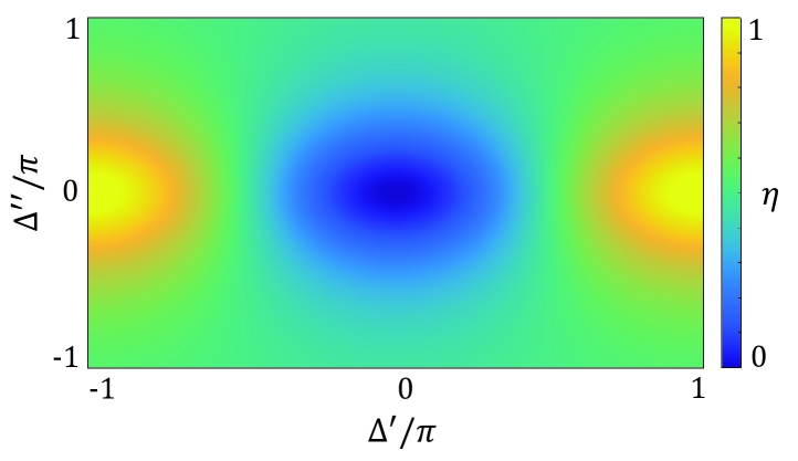
In practice, dielectrics offer the advantage of possible transparency over very a large spectral range, which favors the elaboration of high-transmission devices. On the other hand, high-refractive indices enable optimal cross-polarization conversion with thin layers with respect to wavelength. Besides the average refractive index mismatch between the external and structured media and the average attenuation that both affect the overall transmission, the dichroism (i.e., the anisotropy of the imaginary part of the complex dielectric permittivity tensor) has a direct influence on the helicity transformation . More precisely, the purity parameter defined as the fraction of the output power that corresponds to helicity-flipped field experiencing the Pancharatnam-Berry phase can be expressed as Hakobyan (2016) where and , with the wavevector in vacuum, the thickness of the element, its complex refractive index and referring to direction parallel and perpendicular to the local effective optical axis. Interestingly, the dichroism may enhance or reduce the purity depending on the real birefringent phase retardation, as illustrated in Fig. 1.
Here we propose an unexplored yet approach for the fabrication of dielectric geometric phase optical elements based on femtosecond DLW of photo-resists, although the technology is now mature Malinauskas et al. (2013). An asset of this approach is that it is easy-to-implement while the realization of macroscopic dimensions is possible. This contrasts to currently employed nanofabrication techniques based on electron beam lithography, focused ion milling, and atomic layer deposition of dielectric layers that remain the privilege of cleanroom facilities and require high-level technical support. Moreover, the inherent three-dimensional structuring capabilities of proposed approach allows considering the fabrication of dielectric devices on curved and flexible substrates Malinauskas et al. (2016) while the structured material itself can be reconfigurable under external forcing for instance by using elastomers Yin et al. (2016). In present case, we choose the hybrid (20% inorganic, 80% organic) photo-resist SZ2080 whose refractive index is over the nm wavelength range Žukauskas et al. (2015). Such a material has a low shrinkage, high optical transmissivity, and is widely used for micro-optical elements Ovsianikov et al. (2008); Brasselet et al. (2010); Balčytis et al. (2016); Rekštytė et al. (0155). In principle, highly pure geometric phase optical elements can thus be formally obtained under appropriate optimization of the designed structure following above discussion on the parameter .
Without lack of generality, we restrict our demonstration to the realization and characterization of spin-to-orbital optical angular momentum converters. Such elements correspond to azimuthally varying optical axis orientation of the form ( half-integer and the polar angle in cylindrical coordinates) with, ideally, uniform real birefringent phase retardation of Marrucci et al. (2006b). In turn, a spin-orbit coupler transforms an incident field with helicity (that is associated with spin angular momentum per photon) into an helicity flipped field endowed with a spatial distribution of the phase of the form (that is associated with orbital angular momentum per photon). The choice of such a design to test our approach is motivated by the wide range of applications in classical and quantum optics of these so-called -plates Marrucci et al. (2011) that have become a prototypical benchmark for geometric phase optical elements.
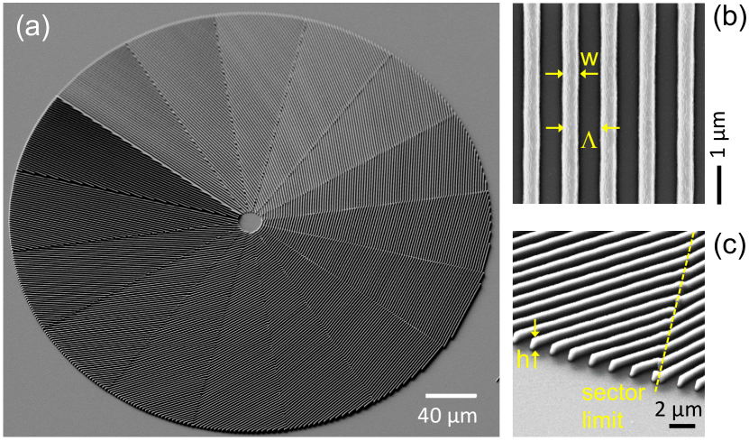
The DLW experimental platform basically consists of a regenerative amplified Yb:KGW based femtosecond fs-laser system (Pharos, Light Conversion Ltd.) operating at the second harmonic wavelength of 515 nm with pulse duration of 230 fs and 200 kHz repetition rate. The laser beam is focused with an oil-immersion objective lens of numerical aperture (Olympus) onto the interface of a cover glass on which the dielectric photo-resist doped with 1%wt. 4,4’-bis-diethylaminobenzophenone as a photoinitiator is drop-casted and dried under room temperature for 12 h before laser writing. The pulse energy after the objective is set to 0.12 nJ at the scanning speed of 0.1 mm/s. After fabrication, the samples were developed in a methyl-isobutyl-ketone and isopropanol 1:2 solution for 10 min followed by a 1 min acetone bath and 10 min rinse in isopropanol. Then, the structures were dried on a hotplate at 50∘C for 10 min. Finally, a 5-nm-thick film of titanium was sputtered for structural characterization by scanning electron microscopy (SEM).
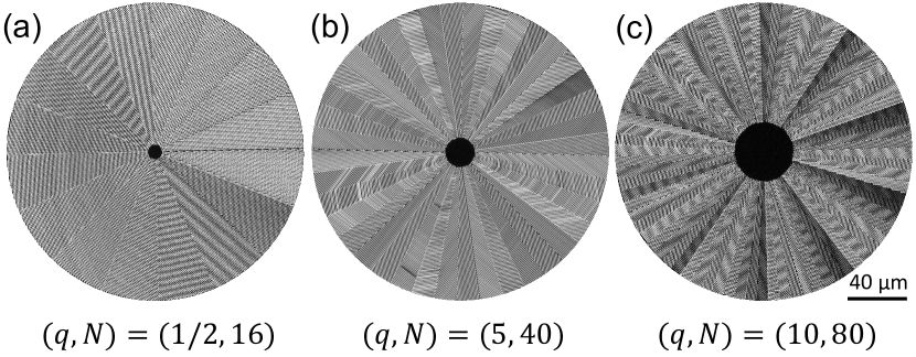
A -step discrete design is chosen for the space-variant grating structure associated with a pitch m and filling factor defined by the width-to-period ratio of the gratings , as illustrated in Fig. 2 for and . High-charge elements have also been fabricated, as shown on Fig. 3 for , and that correspond to fabrication time around 10, 35 and 40 min, respectively, which is acceptable for industrial DLW. In practice, patterns of lower complexity and centimeter square area can be made in several hours using faster scanning and higher laser repetition rate.
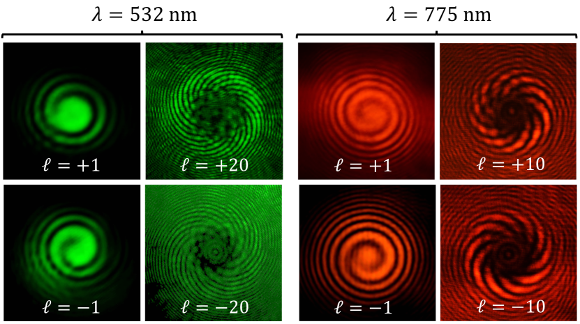
The optical characterization of the fabricated spin-to-orbital couplers is made by inspecting the spiraling phase profile imprinted by the structures to the contra-circularly polarized output field component. In practice this is made in a straightforward manner by illuminating the sample by a -polarized collimated beam of typical diameter 1 mm and subsequent polarization imaging the intensity distribution of the field that emerges from the sample. Indeed, the diffraction of light on the finite size -plate having central unstructured area (see Fig. 3) leads to “single-beam interferometry” by providing coaxial overlap between the two circularly polarized output field components, hence without need of an external reference beam. This leads to spiraling fringes patterns whose contrast is optimized by adjusting the polarization state on which the total field is projected. This is made by placing an achromatic quarter-waveplate followed by a polarizer after the sample and adjusting their relative orientation. The results are illustrated in Fig. 4 for the structures shown in Fig. 3 at two different wavelengths (532 nm and 775 nm) and for incident helicity . As expected, -arm spiraling patterns with helicity-dependent handedness are observed, which demonstrates the generation of optical vortex beams associated with an optical phase singularity of topological charge .
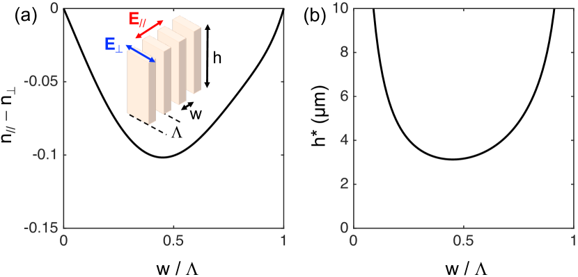
On the other hand, the performance of the photo-polymerized geometric phase optical elements is experimentally evaluated to a few percents. Although such a modest value does not compromise the proof-of-principle that femtosecond DLW of photo-polymeric materials is an approach that is worth to explore further, this invites to consider how to optimize it. For this purpose, an option is to calculate the complex form birefringence phase retardation , which can be done by using effective medium theories or brute force FDTD simulations. In practice, inherent resolution of the DLW technique is restricted to in the visible range, see for instance Ref. Cheng et al. (2014) reporting on grating pitch nm using standard DLW while twice smaller values are accessible to super-resolution DLW techniques Fischer and Wegener (2013). In turn, second-order effective medium theory appears as a relevant, yet simple, analytical tool to design an optimal structure if grating pitch is small enough. Indeed, the latter approach is typically considered valid up to Emoto et al. (2010). Although chosen parameters for present experimental demonstration are obviously not optimal, it is instructive to have a look on expected parameters enabling optimal performances. This is done by applying second-order effective medium theory, see Eqs. (1) and (2) of Ref. 26, assuming for the sake of illustration with nm and . One gets an optical anisotropy that depends on the filling factor according to Fig. 5(a) where and are the effective refractive indices parallel and perpendicular to the grating wavevector lying in the plane of the structure. Then, the optimal height satisfying the optimal birefringent phase retardation is evaluated from , see Fig. 5(b). The latter optimized structure height is in the range m for filling factor in the range , which implies design flexibility. However, the ability to fabricate polymerized line with aspect ratio should not be eluded and certainly deserves further work to validate robust processing solutions, since structures with aspect ratio of 18 have been recovered by a wet bath development of a negative resist Kondo et al. (2005) and even more delicate structures can be retrieved by avoiding the capillary forces via a critical point drying process Malinauskas et al. (2016). In practice, such conclusions regarding the optimal purity still applies qualitatively in case of moderate dichroic losses (say ) as shown in Fig. 1.
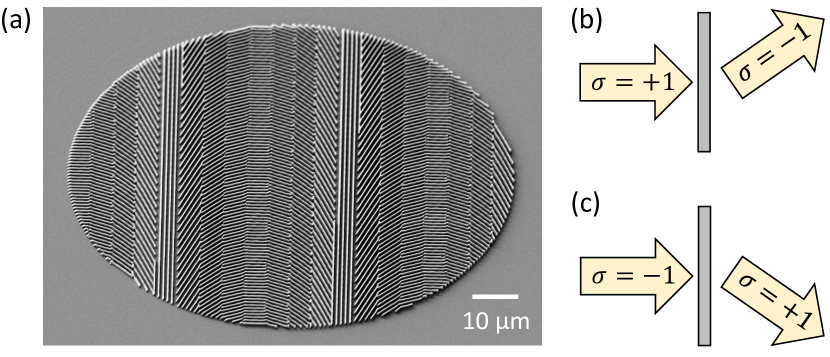
As said above, geometric phase optical elements are not restricted to spin-to-orbital angular momentum couplers and DLW technology is versatile. This is illustrated in Fig. 6(a) that shows SEM image of a discretized optical spin splitter enabling helicity dependent redirection of light. Such a device consists of a one-dimensional grating orientation angle distribution of the form leading to a tilt of an incident phase front of the contra-circular output component, as depicted in Figs. 6(a) and 6(c) for .
In summary, we proposed a novel technique to fabricate geometric phase optical elements using femtosecond direct laser writing of photo-resists. The approach is demonstrated by realizing spin-orbit optical vortex generators of topological charge from 1 to 20 and optical spin splitters. Such space-variant form-birefringent structures basically work over a broad spectral range, though at the expense of overall efficient since the optimal birefringent phase retardation condition is satisfied only for well-defined frequencies. In other words, the very same design principle is applicable for IR and THz spectral ranges, where application potential is likely for sensing applications. More generally, by enriching the geometric phase optical elements toolbox with a nowadays matured technology, our results contributes to the further developments of spin-orbit photonics.
We acknowledge Workshop of Photonics R&D. Ltd. for the laser fabrication setup acquired via a collaborative grant. We are grateful to Mangirdas Malinauskas for discussions on laser printing conditions. Partial support by the NATO grant SPS-985048, the Australian Research Council DP130101205 and DP170100131 Discovery projects is also acknowledged.
References
- Bhandari (1997) R. Bhandari, Phys. Rep. 281, 1 (1997).
- Pancharatnam (1956) S. Pancharatnam, Proc. Indian Acad. Sci. Sect. A 44, 247 (1956).
- Berry (1987) M. V. Berry, J. Mod. Opt. 34, 1401 (1987).
- Biener et al. (2001) G. Biener, V. Kleiner, and E. Hasman, Opt. Lett. 26, 1424 (2001).
- Biener et al. (2002) G. Biener, A. Niv, V. Kleiner, and E. Hasman, Opt. Lett. 27, 1875 (2002).
- Marrucci et al. (2006a) L. Marrucci, C. Manzo, and D. Paparo, Appl. Phys. Lett. 88, 221102 (2006a).
- Kim et al. (2015) J. Kim, Y. Li, M. N. Miskiewicz, C. Oh, M. W. Kudenov, and M. J. Escuti, Optica 2, 958 (2015).
- Beresna et al. (2011) M. Beresna, M. Gecevicius, P. G. Kazansky, and T. Gertus, Appl. Phys. Lett. 98, 201101 (2011).
- Lin et al. (2014) D. Lin, P. Fan, E. Hasman, and M. L. Brongersma, Science 345, 298 (2014).
- Desiatov et al. (2015) B. Desiatov, N. Mazurski, Y. Fainman, and U. Levy, Opt. Express 23, 22611 (2015).
- Kruk et al. (2016) S. Kruk, B. Hopkins, I. I. Kravchenko, A. Miroshnichenko, D. N. Neshev, and Y. S. Kivshar, Appl. Phys. Lett.: Photonics 1, 030801 (2016).
- Devlin et al. (2016) R. C. Devlin, M. Khorasaninejad, W. T. Chena, J. Oh, and F. Capasso, Proc. Natl. Acad. Sci. USA 113, 10473 (2016).
- Hakobyan (2016) D. Hakobyan, Spin-orbit optomechanics of space-variant birefringent media, Ph.D. thesis, University of Bordeaux and Swinburne University of Technology (2016).
- Malinauskas et al. (2013) M. Malinauskas, M. Farsari, A. Piskarskas, and S. Juodkazis, Phys. Rep. 533, 1 (2013).
- Malinauskas et al. (2016) M. Malinauskas, A. Žukauskas, S. Hasegawa, Y. Hayasaki, V. Mizeikis, R. Buividas, and S. Juodkazis, Light: Sci. Appl. 5, e16133 (2016).
- Yin et al. (2016) D. Yin, J. Feng, R. Ma, Y.-F. Liu, Y.-L. Zhang, X.-L. Zhang, Y.-G. Bi, Q.-D. Chen, and H.-B. Sun, Nature Comm. 7, 11573 (2016).
- Žukauskas et al. (2015) A. Žukauskas, M. Malinauskas, E. Brasselet, and S. Juodkazis, “3d micro-optics via ultrafast laser writing: miniaturisation, integration, and multifunctionalities,” in Three-Dimensional Microfabrication Using Two-Photon Polymerization, edited by T. Baldacchini (2015) Chap. 12.
- Ovsianikov et al. (2008) A. Ovsianikov, J. Viertl, B. Chichkov, M. Oubaha, B. MacCraith, I. Sakellari, A. Giakoumaki, D. Gray, M. Vamvakaki, M. Farsari, and C. Fotakis, ACS Nano 2, 2257 (2008), http://dx.doi.org/10.1021/nn800451w .
- Brasselet et al. (2010) E. Brasselet, M. Malinauskas, A. Žukauskas, and S. Juodkazis, Appl. Phys. Lett. 97, 211108 (2010).
- Balčytis et al. (2016) A. Balčytis, D. Hakobyan, M. Gabalis, A. Žukauskas, D. Urbonas, M. Malinauskas, R. Petruškevičius, E. Brasselet, and S. Juodkazis, Opt. Express 24, 16988 (2016).
- Rekštytė et al. (0155) S. Rekštytė, T. Jonavicius, D. Gailevičius, M. Malinauskas, V. Mizeikis, E. G. Gamaly, and S. Juodkazis, Adv. Opt. Mat. 4 (2016 (online published DOI: 10.1002/adom.201600155)).
- Marrucci et al. (2006b) L. Marrucci, C. Manzo, and D. Paparo, Phys. Rev. Lett. 96, 163905 (2006b).
- Marrucci et al. (2011) L. Marrucci, E. Karimi, S. Slussarenko, B. Piccirillo, E. Santamato, EleonoraNagali, and F. Sciarrino, J. Opt. 13, 064001 (2011).
- Cheng et al. (2014) Y. C. Cheng, H. Zeng, J. Trull, C. Cojocaru, M. Malinauskas, T. Jukna, D. S. Wiersma, and K. Staliunas, Opt. Letters 39, 6086 (2014).
- Fischer and Wegener (2013) J. Fischer and M. Wegener, Laser Photonics Rev. 7, 22 (2013).
- Emoto et al. (2010) A. Emoto, M. Nishi, M. Okada, S. Manabe, S. Matsui, N. Kawatsuki, and H. Ono, Appl. Opt. 49, 4355 (2010).
- Kondo et al. (2005) T. Kondo, S. Juodkazis, and H. Misawa, Appl. Phys. A 81, 1583 (2005).