Resonant Raman imaging of MoS2-substrate interaction
Abstract
We report a study of long-range MoS2 -substrate interaction using resonant Raman imaging. We observed a strong thickness-dependent peak shift of a Raman-forbidden mode that can be used as a new method of determining the thickness of multilayered MoS2 flakes. In addition, dependence of the Raman scattering intensity on thickness is explained by the interference enhancement theory. Finally, the resonant Raman spectra on different substrates are analysed.
Keywords: MoS2, resonant Raman, AFM, thickness-dependence, forbidden mode
I Introduction
Two-dimensional (2D) transition metal dichalcogenide (TMD) materials have recently attracted wide attention due to their potential applications in optoelectronic devices. For example, monolayer MoS2 has a large direct band gap Splendiani et al. (2010), and can be used in field-effect-transistorsLin et al. (2013). As a powerful tool, Raman spectroscopy has been widely used for studying the various properies of MoS2. Frey studied the resonant Raman (RR) spectra of MoS2 nanoparticles Frey et al. (1999). Li and Chakraborty have investigated the thickness-dependent effects for the Raman scattering of MoS2 Chakraborty et al. (2013); Li et al. (2012a). Also, the influence of the substrate-MoS2 interactions on the Raman spectra has been investigated Buscema et al. (2014). In this paper, we performed RR imaging of multilayered MoS2 flakes using 660 nm laser excitation which corresponds to the A exciton of MoS2 Coehoorn et al. (1987); Acrivos et al. (1971). We obtained simultaneously the topographic information and correlated it with Raman imaging. The correlated AFM-Raman imaging reveals the relation between the thickness and optical properties. We also analysed the influence of substrates with different dielectric properties on the RR spectra of MoS2 .
II Results
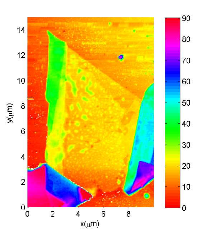
The multilayered MoS2 flakes were exfoliated on SiO2 and gold substrate using the scotch-tape method. Th AFM image of a typical MoS2 flake is shown in Fig.1 (a). The thinnest part of the flake has the height of 3nm, which corresponds to 5 layers of MoS2 Chakraborty et al. (2013). Note the colorbar in Fig.1 (a) corresponds to the number of layers .
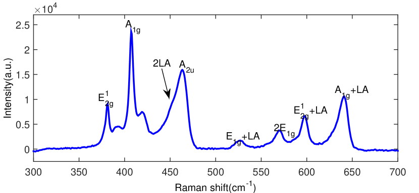
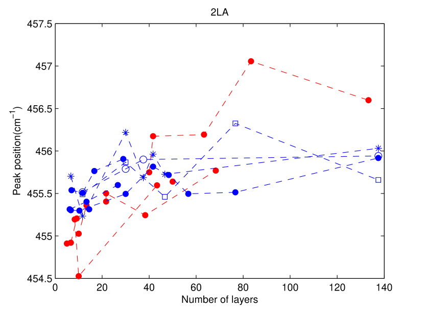
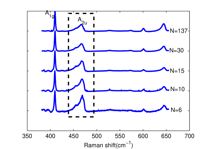
A typical RR spectrum of the MoS2 flake is shown in Fig.1 (b). The main spectral features include: strong out-of-plane A1g mode near 410cm-1 , in-plane mode near 385cm-1 , IR-active A2u mode near 466cm-1 and several second-order modes, which include E1g+LA at 528cm-1 , 2E1g at 574cm-1 , E+LA at 600cm-1 and A1g+LA at 644cm-1 Chakraborty et al. (2013); Frey et al. (1999).
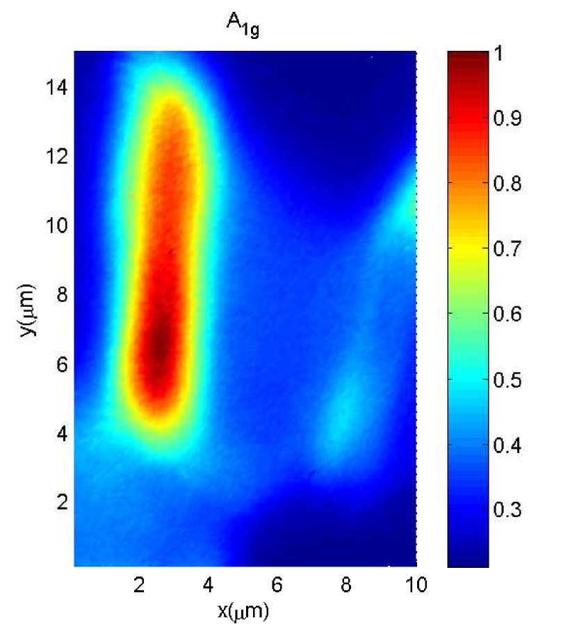
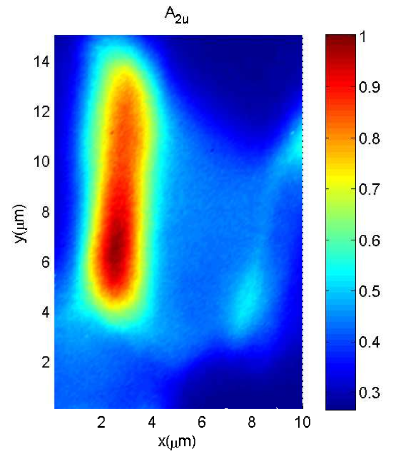
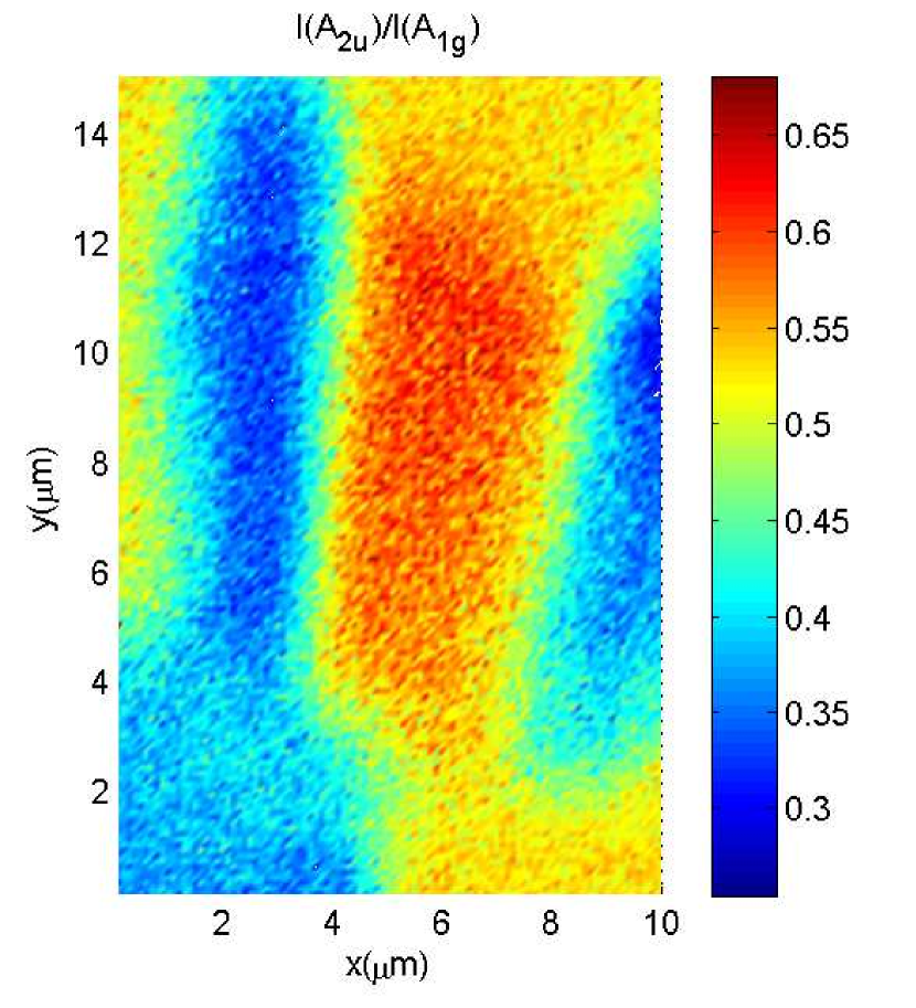
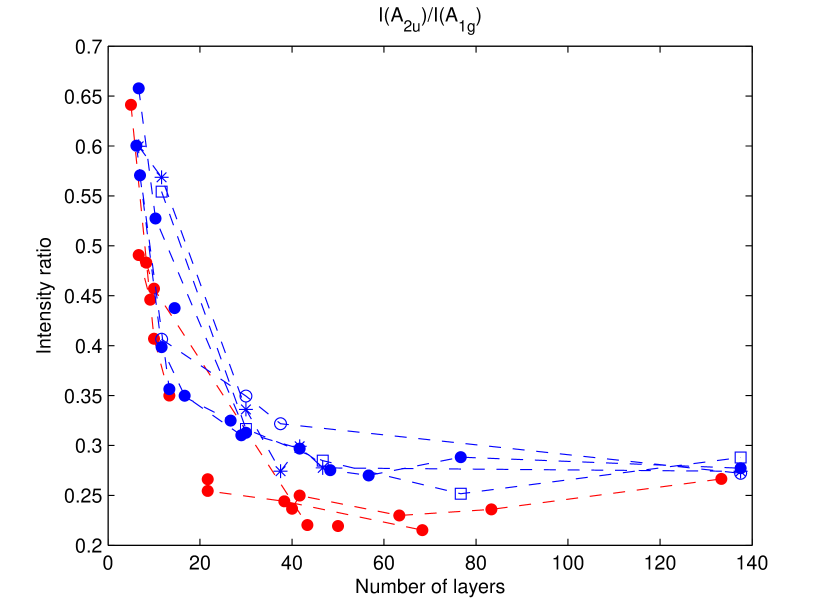
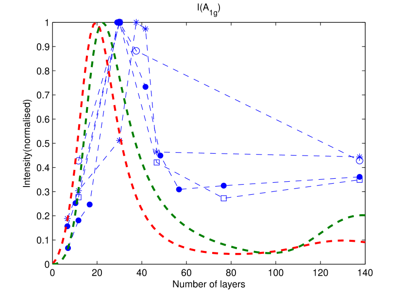
Resonant Raman imaging of the multilayered MoS2 flake on the gold substrate is shown in Fig.2. The imaging step size was 100nm. The intensity maps for A1g and A2u modes are shown in Fig.2 (a) and (b). The intensity ratio I(A2u )/I(A1g ) is shown in Fig.2 (c). Both Fig.2 (a) and (b) show that the area with the strongest intensity corresponds to the number of layers of about 30, while the very thin (eg: the middle) and the very thick (eg: the left bottom) parts of the flake show a relatively low intensity. I(A1g ) vs the number of layers is shown in Fig.4 (b) where the maximum intensity correspond to n=30. The intensity ratios in Fig.4 (a) and Fig.5 indicate that for the thin part, the A2u peak has a relatively stronger intensity compared to other modes.
(a)
(b)
(a)
(b)
(c)
(d)
(e)
(f)
(a)
(b)
(c)
(a)
(b)
(a)
(b)
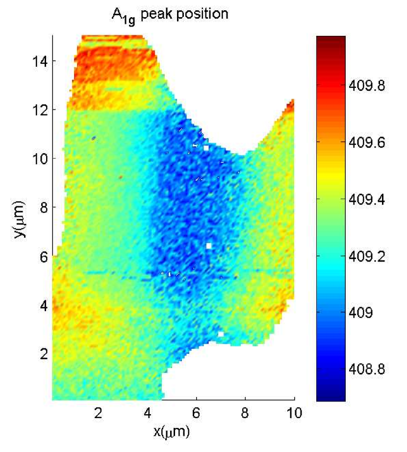
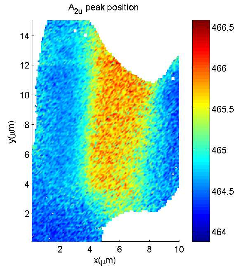
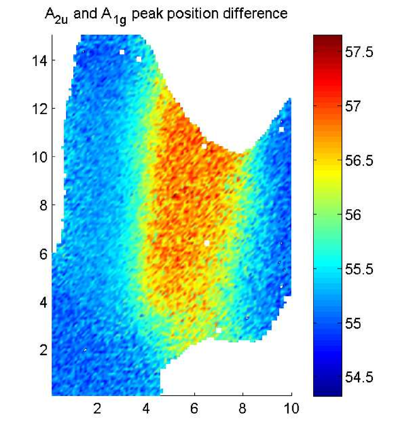
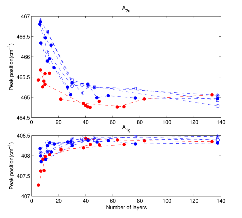
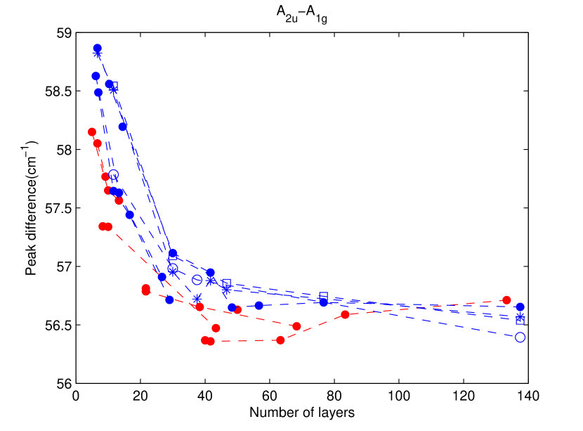
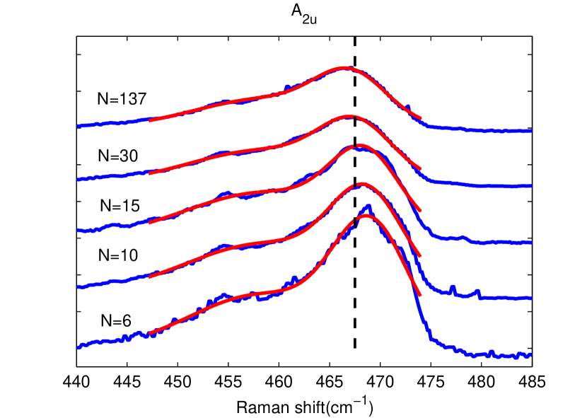
Peak positions also show shifts with the change of the number of layers . The peak position maps of the A1g and A2u modes are shown in Fig.2 (d) and (e). Combined with the height distribution in Fig.1 (a), the RR spectra show a blue shift for A1g and a red shift for A2u for a multilayered flake compared to bulk MoS2 . Fig.3 (a) and (b) show the A1g and A2u peak position versus the number of layers . The A1g peak position increases slightly(0.5cm-1 ) when the number of layers increases from 7 to 140, while the A2u peak has a blue shift of about 2cm-1 . The shift of the A2u peak can seen more clearly in Fig.5 (a) and (b).
III Discussion
We consider two main effects: (1) substrate dependence, (2) thickness-dependence, including peak shifts and intensity variations. It has been widely reported that, on common insulating substrates such as silicone and SiO2, the increase of the number of layers has an influence on the two characteristic Raman peaks Eand A1g Chakraborty et al. (2013); Li et al. (2012b). The A1g mode has a blue shift due to the increase of the force constant which is induced by the increased interlayer van der Waals interaction. Our RR measurements of the A1g peak position variation are consistent with the previous reports. However, here we show that, under the resonant condition, the Raman-inactive A2u mode shows a strong thickness-dependent softening with the increase of the number of layers . This is attributed to the decrease of the long-range Coulombic interaction between the Mo atoms with increasing layer number Sanchez and Wirtz (2011). The results on SiO2 substrate are consistent with previous reports. For the small number of layers (n10), the thickness-dependent RR signal of both A1g and A2u mode show red shifts with the increase of the number of layers Chakraborty et al. (2013). When the number of layers exceeds 10, the change of the peak position is small and difficult to measure.
However on the gold substrate, we observed a previously unreported blue shift for the A2u mode. Fig.3 (a) shows that for a small number of layers (), the A2u peak has a red shift of about 2cm-1 compared to the bulk MoS2 . With the increase of the thickness, this red shift gradually disappears with a turning point near , as shown in Fig.3 (a). This indicates that the thickness-dependent effects can be observed within a large range of the number of layers . This is different from the SiO2 substrate where the peak shift can only be observed for a small number of layers (n10).
We consider two possible reasons for the different peak shift directions of the A2u mode of the multilayered MoS2 flake on the gold substrate: (1) laser-induced heating of the gold substrate may have thermal effects on MoS2 leading to the peak shift Najmaei et al. (2014); (2) charge transfer from MoS2 to the gold substrate modifying the doping, and the electron-phonon interactions Buscema et al. (2014); Bhanu et al. (2014). We discard the first possibility by performing laser power dependent measurements. Different laser power can lead to different surface temperatures. However, we find no observable changes in the peak position vs the number of layers for different laser powers (Fig.3). The second possible explanation may be supported by previous literature reports which considered the non-resonant situation. Several studies reported p-doping of MoS2 using various methods, including deposition on the gold substrate Buscema et al. (2014); Robinson et al. (2015), decoration with gold nano-particles (NP) Y.Shi et al. (2013), and using monolayer MoS2 transistor to adjust the doping level directly Chakraborty et al. (2012) resulting in stiffening of the A1g mode. Here our results show the corresponding blue shift of the A1g mode on the gold substrate for the number of layers N<10, which is consistent with the previous studies. Here, we, for the first time, observed that under the resonant conditions, the Raman-inactive A2u mode of MoS2 on the gold substrate shows a strong blue shift compared with that on the SiO2 substrate. Fig.3 (a) shows a shift more than 1cm-1 when the number of layers is less than 10 layers.
Fig.4 shows the nearly linear increase of the A1g peak intensity until the number of layers reaches 30 with the maximum point n=30, followed by a decrease until n=50. Note that the Raman signal intensity of bulk MoS2 is weaker than that with the number of layers of 30. This may be attributed to the inference enhancementWang et al. (2008); Ni et al. (2008) due to multiple reflections of the incident laser and emitted Raman signals in MoS2 flakes. Using the model of Wang , the intensity of the Raman signal can be expressed as
| (1) |
where is the thickness of the MoS2 flake, is the amplitude of the electric field at the depth , and is the enhancement factor due to the multiple-reflection. The simulation is shown as a red dashed line in Fig.3 (b). The original model assumes no coherence between the field scattered from adjacent layers. Considering coherence, Eq. (1) can be written as
| (2) |
The coherent simulation is different, shown as a green dashed line in Fig.3 (b). Zeng provided a qualititative explanation by using the accumulated phase shift for the reflected field and destructive interference with the first reflected field from the flake surface J.Zeng et al. (2015).
acknowledgements
We thank Profs. Marlan Scully, Alexei Sokolov and Zhenrong Zhang for helpful discussions. We also thank Prof. Marlan Scully for the access to Raman facilities and we thank Zhenrong Zhang for help with sample preparation. D.V. acknowledges the support of NSF grant CHE-1609608.
References
- Splendiani et al. (2010) A. Splendiani, L. Sun, Y. B. Zhang, T. S. Li, J. Kim, C. Y. Chim, G. Galli, and F. Wang, Nano Lett. 10, 1271 (2010).
- Lin et al. (2013) J. Lin, H. Li, H. Zhang, and W. Chen, Appl. Phys. Lett. 102, 203109 (2013).
- Frey et al. (1999) G. L. Frey, R. Tenne, M. J. Matthews, M. Dresselhaus, and G. Dresselhaus, Physical Review B 60, 2883 (1999).
- Chakraborty et al. (2013) B. Chakraborty, H. S. S. R. Matte, A. K. Sood, and C. N. R. Rao, J. Raman Spectrosc. 44, 92 (2013).
- Li et al. (2012a) H. Li, Q. Zhang, C. C. R. Yap, B. K. Tay, T. H. T. Edwin, A. Olivier, and D. Baillargeat, Advanced Functional Materials 22, 1385 (2012a).
- Buscema et al. (2014) M. Buscema, G. A. Steele, H. S. J. van der Zant, and A. Castellanos-Gomez, Nano Res. 7, 561 (2014).
- Coehoorn et al. (1987) R. Coehoorn, C. Hass, and R. A. de Groot, Phys. Rev. B 35, 6023 (1987).
- Acrivos et al. (1971) J. V. Acrivos, W. Y. Liang, J. A. Wilson, and A. D. Yoffe, J. Phy. C 4, L18 (1971).
- Li et al. (2012b) H. Li, Q. Zhang, C. C. R. Yap, B. K. Tay, T. H. T. Edwin, A. Olivier, and D. Baillargeat, Adv. Funct. Mater. 22, 1385 (2012b).
- Sanchez and Wirtz (2011) A. M. Sanchez and L. Wirtz, Phys. Rev. B 84, 155413 (2011).
- Najmaei et al. (2014) S. Najmaei, A. Mlayah, A. Arbouet, C. Girard, J. Leotin, and J. Lou, NANO 8, 12682 (2014).
- Bhanu et al. (2014) U. Bhanu, M. R. Islam, L. Tetard, and S. I. Khondaker, Sci. Rep. 4, 5574 (2014).
- Robinson et al. (2015) B. J. Robinson, C. E. Giusca, Y. T. Gonzalez, N. D. Kay, O. Kazakova, and O. V. Kolosov, 2D Materials 2, 015005 (2015).
- Y.Shi et al. (2013) Y.Shi, J. Huang, L. Jin3, Y. Hsu, S. Yu, L. Li, and H. Yang, Scientific Reports 3, 1839 (2013).
- Chakraborty et al. (2012) B. Chakraborty, A. Bera, D. Muthu, S. Bhowmick, U. V. Waghmare, and A. Sood, Phys. Rev. B 85, 161403 (2012).
- Wang et al. (2008) Y. Y. Wang, Z. H. Ni, Z. X. Shen, H. M. Wang, , and Y. H. Wu, Appl. Phys. Lett. 92, 043121 (2008).
- Ni et al. (2008) Z. Ni, Y. Wang, T. Yu, and Z. Shen, Nano Res 1, 273 (2008).
- J.Zeng et al. (2015) J.Zeng, J. Li, H. Li, Q. Dai, S. Tie, and S. Lan, Optics Express 23, 31817 (2015).