Brightening of dark excitons in monolayers of semiconducting transition metal dichalcogenides
Abstract
We present low temperature magneto-photoluminescence experiments which demonstrate the brightening of dark excitons by an in-plane magnetic field applied to monolayers of different semiconducting transition metal dichalcogenides. For both WSe2 and WS2 monolayers, the dark exciton emission is observed at 50 meV below the bright exciton peak and displays a characteristic doublet structure which intensity is growing with , while no magnetic field induced emission peaks appear for MoSe2 monolayer. Our experiments also show that the MoS2 monolayer has a dark exciton ground state with a dark-bright exciton splitting energy of 100 meV.
I Introduction
Monolayers (MLs) of semiconducting transition metal dichalcogenides (S-TMDs) MX2 where MMo or W and XS, Se or Te, are direct band gap semiconductors [1] with the minima (maxima) of conduction (valence) band located at the inequivalent K+ and K- points of their hexagonal Brillouin zone (BZ). These two-dimensional semiconductors host tightly bound excitons with unconventional properties such as binding energies as large as few hundreds of meV and non Rydberg excitation spectrum [2; 3; 4]. The lack of inversion symmetry together with the strong spin-orbit interaction lift the degeneracy between spin levels in the conduction (CB) and valence (VB) bands at the K+ and K- points related by time reversal symmetry. The spin-orbit interaction leads to well separated spin subbands in each valley and to the possibility of initializing a defined valley population with circularly polarized optical excitation [5; 6; 7; 8] or generation of valley coherence [9; 10]. The spin-orbit splitting in the valence is as large as few hundreds of meV [11; 12; 13; 14; 3; 15; 16; 17; 18; 19; 20; 21; 22] while its counterpart in the conduction band is predicted to be of the order of few tens of meV only. What is however important is that can be positive or negative [23; 24] and in consequence, two distinct ordering of the spin orbit split CB subbands are feasible [25; 26; 27].
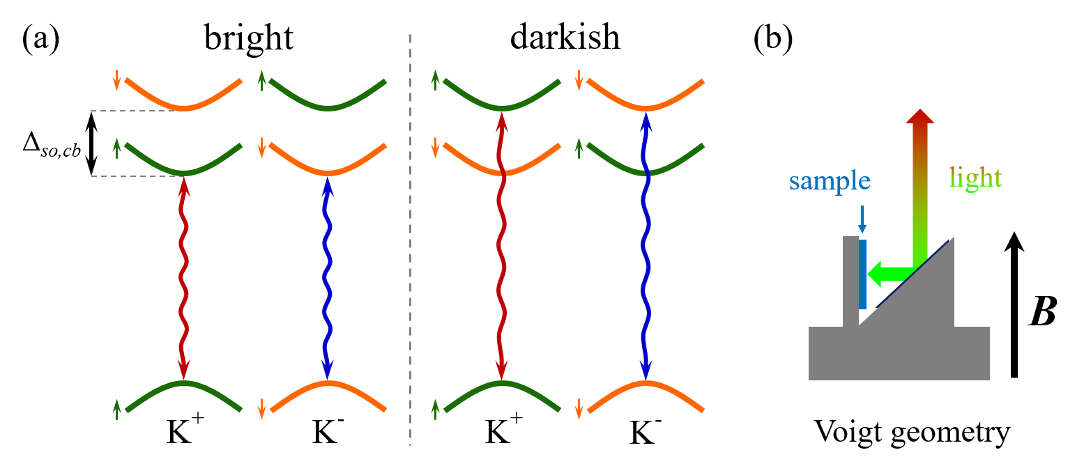
Because optical transitions in S-TMDs do conserve the spin, different orderings of electronic bands in the conduction band have profound consequences on their optical properties. Depending on the sign of , the excitonic ground state can be bright (parallel spin configuration for the top VB and the lowest CB subbands between which the optical transition is allowed) or dark (anti-parallel spin configuration and optically forbidden ground state interband transition). The ordering of the electronic bands, characteristic for these two monolayer families, referred to as bright and darkish ones, are illustrated in Fig. 1(a). Theoretical studies [25; 26; 27] indeed predict that monolayers of MoSe2 and of MoTe2 should be bright (>0 to set a convention) while WSe2 and WS2 monolayers are darkish (<0). Yet, there is no general consensus concerning the bright of darkish character of a MoS2 monolayer. The theoretical works reported in Refs 26; 27 classify the MoS2 monolayer as a bright system: >0 but as small as meV. Instead, another theoretical study [28] indicates that MoS2 monolayers are rather darkish ().
A detailed knowledge of the exciton fine structure is crucial for S-TMD based optoelectronic devices and for valleytronic applications, as i) optical properties strongly depend on the type of excitonic ground state, and ii) scattering mechanisms, and in particular intervalley scattering mechanisms, can have much different efficiencies for bright and dark excitons [29; 30]. On the experimental point of view, recent optical studies of WSe2 have shown that the temperature dependence of its PL intensity is consistent with a dark excitonic ground state and the dark-bright exciton splitting of about meV has been experimentally estimated from temperature activation type analysis [31; 32; 33].
Magnetic fields, applied in an adequate configuration with respect to a crystal axis, can mix electronic wave functions and thus the excitonic states which are built out of these wave functions. This effect triggered the spectroscopy of optically dark excitons in a large variety of condensed matter systems, ranging from bulk semiconductors [34], semiconductor quantum dots [35; 36], to single wall carbon nanotubes [37; 38]. One expects that also in monolayers of S-TMDs, the in-plane magnetic field acts as a perturbation to the system’s Hamiltonian, mixing the two lowest spin levels in the CB and hence, the bright excitons giving some optical activity to the initially dark excitonic states [39].
In this paper, we provide a direct measurement of the dark exciton emission in darkish monolayers of S-TMDs by mixing the spin levels of bright and dark excitons by an in-plane magnetic field. Dark excitons appear in the low temperature magneto-photoluminescence (PL) spectra as clear features growing with the magnetic field at energies lower than that of the bright exciton. This observation gives a direct access to the values of dark-bright exciton splitting in WSe2 and WS2 monolayers. In the case of MoSe2, no significant change in the emission spectrum is observed when applying a magnetic field, in agreement with its bright exciton ground state. MoS2 is shown to belong to the family of darkish materials with a dark-bright splitting energy close to meV. The emission intensity of dark excitons increases as , in accordance with their perturbative activation by the in-plane magnetic field.
II Theoretical Background
To examine the band edge interband transitions in S-TMD monolayers we consider the top VB and two spin-orbit split CB subbands [see Fig. 1(a)]. Associated with these subbands and relevant for our considerations are intravalley interband transitions (intravalley A excitons) which involve the states from the the same K+ or K- valley. Four types of intravalley A excitons can be distinguished and labelled according to their valley and CB spin indices (the VB spin index, is fixed to in valley and in valley). The configurations with from the K+ valley and from the K- valley correspond to optically active, bright A excitons, referred to as . The configurations with from the K+ valley and from the K- valley correspond to optically inactive, dark A excitons, refereed to as .
The ground state of bright (darkish) S-TMD monolayers is then formed from bright (dark) A excitons. Because these quasi-particles differ from each other by their spin configuration in the CB, spin-flip processes in the CB can make the dark states optically active and can allow for investigations of the ground state of darkish materials.
A magnetic field , applied along the plane of a S-TMD monolayer, mixes the spin states in the CB and VB via the Zeeman interaction. Since , the spin-mixing in the VB can be neglected. The Zeeman term acting on the CB states can be expressed as:
| (1) |
Here is the in-plane gyromagnetic ratio for the CB, is the Bohr magneton and are the Pauli matrices in the CB spin subspace. The in-plane magnetic field results in the mixing of the dark and bright excitons. It can be described by an effective Hamiltonian in the basis of {, }, obtained by the projection of spin states of the CB, mixed by the magnetic field, on the exciton states
| (2) |
Here we introduced . and are the energies of the bright and dark excitons in the absence of an external magnetic field, . The application of the in-plane magnetic field does not lift the double degeneracy of each dark and bright exciton states as does not depend on valley index .
Assuming that the Zeeman term gives a small correction to the basic exciton states, we obtain the mixed eigenstates up to second order in magnetic field:
| (3) | |||||
| (4) |
Here . Their eigenenergies are very close to the energies of the dark and bright excitons (the correction is ).
The admixture of bright states to the dark exciton state makes the latter resonance to be possibly observed in the PL spectra when the in-plane magnetic field is applied to the layer. The intensity of such a PL line can be expected to be proportional to the fraction of bright exciton in the corresponding mixed state and to the population of dark excitons:
| (5) |
where is the intensity of the pure bright exciton state emission in the absence of the magnetic field. With available magnetic fields, the factor remains rather small and dark excitons can hardly be observed in absorption experiments. We note two different situations. i) For bright materials, such as MoSe2 or MoTe2, the energy of dark excitons is larger than the energy of the bright ones. Therefore, at low temperatures, the population of dark excitons is suppressed by a Boltzmann factor and optical transitions are mainly due to low-lying bright exciton states. In this case the observation of dark excitons at low temperature is extremely unlikely. ii) For darkish materials, such as WSe2 or WS2, the situation is opposite and the direct observation of dark excitons is possible.
So far we have considered the A excitons formed by the direct electron-hole Coulomb interaction and have not included effects of the exchange part of the Coulomb interaction. The exchange interaction is expected to lift the double valley degeneracy of dark intravalley A excitons due to the presence of a transition dipole moment perpendicular to the monolayer plane, absent for bright excitons [40; 39]. This degeneracy lifting can be viewed as a local-field effect due to the out-of-plane transition dipole moment of spin-forbidden dark excitons. It is analogous to the exchange energy shift of the Z-excitons in semiconductor quantum wells [41; 42]. The resulting energy splitting between the two spin-forbidden dark exciton components in S-TMD monolayers was roughly estimated in Ref. 39 to be about 10 meV; a more precise, microscopic calculation of this splitting is still lacking, to the best of our knowledge. The discussed above effects of the in-plane magnetic field are equally valid for each component of the expected doublet structure of dark excitons in S-TMD monolayers.
III Experimental results and Discussion
Monolayers of S-TMDs have been prepared by mechanical exfoliation of bulk crystals purchased from HQ Graphene. Initially, the flakes were exfoliated onto a polydimethylsiloxane (PDMS) stamp attached to a glass plate. MLs of S-TMDs were then identified by their optical contrast and cross-checked by Raman scattering and PL measurements at room temperature. In order to deposit them on target Si/SiO2(320 nm) substrates, an all-dry PDMS-based transfer method similar to the one described in Ref. 43 was employed.
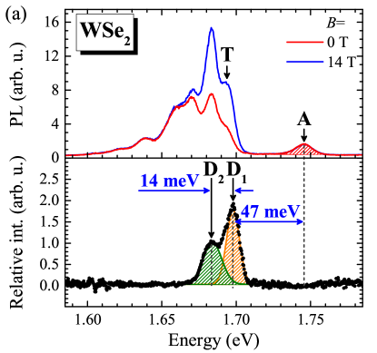
Low temperature magneto-PL experiments were performed in the Voigt configuration [see Fig. 1(b)] using an optical-fiber-based insert placed in a superconducting magnet producing magnetic fields up to T. The samples were placed on top of a x-y-z piezo-stage kept in gaseous helium at K. The light from a semiconductor diode laser (=515 nm) was coupled to an optical fiber with a core of 50 m diameter and focused on the sample by an aspheric lens (spot diameter around 10 m). PL signals were collected by the same lens, injected into a second optical fiber of the same diameter, and analyzed by a m long monochromator equipped with a charge-couple-device (CCD) camera.
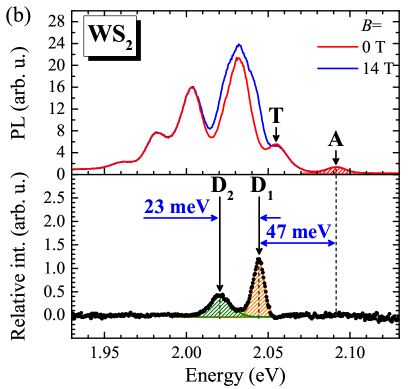
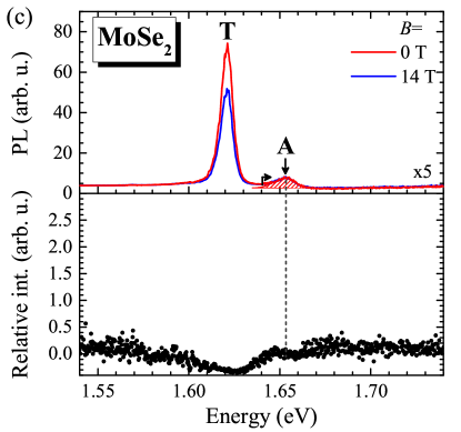
To investigate the effect of an in-plane magnetic field on the PL signal of S-TMD monolayers, we measured the evolution of the low temperature ( K) PL spectra of the WSe2, WS2, MoSe2, and MoS2 MLs in the Voigt configuration as a function of an external magnetic field up to T. The obtained spectra at and at T are presented in the upper panels of Fig. 2. The zero-field PL spectra of all our monolayers display two characteristic emission features, labelled A and T, which are associated with recombination of the neutral [an electron-hole () pair] and charged [an pair + an extra carrier (electron or hole)] excitons formed at the K± points of the BZ [9; 31; 44; 30; 45; 46; 47; 48; 49; 50]. In the case of WSe2, WS2, and also of MoS2, additional features are apparent in the PL spectra in the form of a series of emission lines (WSe2 and WS2) or a broad band (MoS2), at energies below the A exciton energy and overlapping with the T peak. These additional lines have been attributed in the literature to the so-called localized/bound or defect-related excitons [9; 31; 44; 30; 45; 46].
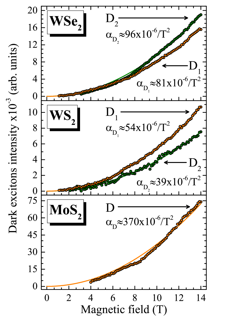
We start with the analysis of the results obtained for the tungsten-based family, WSe2 and WS2 MLs, as both of them are rather firmly predicted to belong to the family of darkish monolayers [25; 26; 27]. The zero-field PL spectra, apart the A and T peaks, consist of several overlapping emission lines on the lower energy side of the spectrum [upper panels of Fig. 2(a) and (b)]. We show in Fig. 2(a) and (b) that the application of a magnetic field in the plane of these monolayers strongly affects their PL spectra at energies meV below the A exciton line. To better visualize the effects of magnetic fields and compare the results obtained for different materials, we define a relative spectrum as (PL - PL)/PL. Such relative intensity spectra for T are presented in the lower panels of Fig. 2(a) and (b). For WSe2 and WS2 MLs, these spectra are composed of two peaks, labelled D1 and D2, which appear on the lower energy side of the bright A exciton. In agreement with our theoretical arguments, these two peaks are assigned to the magnetic-field induced emission due to dark excitons. The higher energy peak, D1, emerges about meV below the A exciton line for both members of the tungsten-based family. The energy separation between the D1 and D2 peaks is meV for WSe2 monolayer and meV for the WS2 monolayer.
To analyze further the data, we fitted the D1 and D2 features using two Gaussian functions [see lower panels of Fig. 2 (a) and (b)]. In the whole range of investigated magnetic fields, the energy and the full width at half maximum (FWHM) of the two D1 and D2 peaks are constant. The brightening of these dark excitons is evidenced by the quadratic evolution of the integrated intensity of these peaks as a function of the magnetic field (, where is a fitting parameter). This behavior is presented in Fig. 3 and is in agreement with the arguments presented in the preceding section (Eq. 5). Important here is the observed dependence and not the precise rates of increase of the two D lines, which apparent values are affected by the chosen normalization of the relative spectra. We consider that the energy difference between the bright A exciton peak and the dark D1 exciton peaks corresponds well to the theoretical predictions of the magnitude [25; 26; 27]. Note that the values for calculated in Ref. 25; 26; 27 do not include the electron-hole Coulomb effects, which obviously affect the interband transition energies but can also significantly influence the apparent bright-dark exciton splitting due to electron-hole exchange effects.
An MoSe2 monolayer is predicted to belong to the family of bright S-TMDs. Its zero-field PL spectra is rather simple (and similar to that observed for MoTe2 monolayers [51]). It is composed of only two A and T features [see Fig. 2(c)][47; 48; 49]. When a magnetic field is applied in the direction along the plane of the layer, no significant changes of the PL spectra are observed. In particular, there are no additional growing structures on the high energy side of the A exciton line, where the dark exciton emission could be expected according to the band ordering at the K± points [see Fig. 1(a)]. The dark exciton emission can not be detected with our experimental conditions as a result of the fast relaxation of carriers to the lowest energy state which is a bright exciton. The only field induced effect observed in the magneto-PL spectra of the MoSe2 monolayer is a small decrease in the intensity of the T-peak [see lower panel of Fig. 2(c)]. The origin of this field induced suppression of the trion emission is not clear for us and calls for a possible theoretical explanation, thought one may speculate that it reflects an influence of the magnetic field on the formation of the charged excitons in a MoSe2 monolayer through a mixing of the spin split bands in both valleys.
Existing models describing the band ordering for MoS2 monolayer largely predict a positive, thought small, meV value for [25; 26; 27], thus placing MoS2 in the family of bright materials. Recently, however, a negative dark-bright exciton splitting has been predicted [28] with a value close to meV. By comparing the PL spectra measured at zero magnetic field for the different materials presented in this study (Fig. 2), the low temperature PL spectrum of MoS2 resembles more the one observed for WS2 and WSe2 than the one of MoSe2 or of MoTe2 [51]. In similarity to the low temperature PL spectra of darkish monolayers, the spectrum of MoS2 also displays a significantly broad emission band at energies lower than that of the A exciton [see Fig. 2(d)]. The observation of either a well defined two peaks PL spectrum arising from the A and T excitons or an additional broad band associated with localized/bound excitons [6; 50], appears to be characteristic of the two families of bright or darkish S-TMD monolayers. The presence of emission due to localized/bound excitons in the low temperature PL of darkish monolayers and not in the bright ones could be due to the appearance of long-lived reservoir of dark excitons in the former systems, which then effectively diffuse and/or relax towards other possible radiative centers. Similar relaxation processes can be largely suppressed in bright monolayers, as the ground state excitons in these systems already represent the effective recombination channel. Following this logic, the ground state exciton should be dark in the MoS2 monolayer.
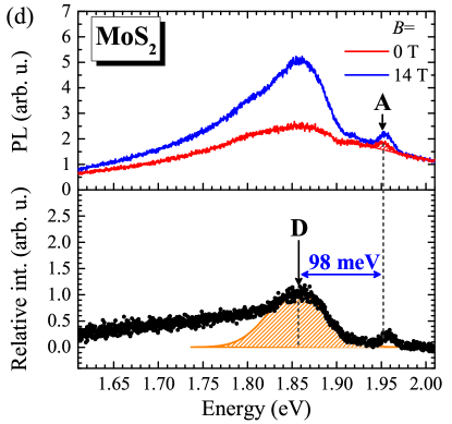
The darkish character of the MoS2 monolayer is confirmed by our magneto-PL study as indeed the in-plane magnetic field has a dramatic effect on the PL spectrum of this monolayer. The relative intensity spectrum displayed in the lower panel of Fig. 2(d) shows a rather single but broad peak, labelled D, which is centered at about meV below the A exciton line of MoS2. Even though all observed PL peaks are much broader in our MoS2 monolayer than in other studied materials, we have performed the same analysis as for the other materials. Similarly to the case of WS2 and WSe2 monolayers, the shape (width and center position) of the relative spectrum of the MoS2 monolayer remain field independent but its amplitude increases quadratically, , with the magnetic field [see Fig. 3]. This result confirm placing the MoS2 in the family of darkish S-TMD with a dark-bright exciton splitting twice bigger than that found in WS2 or in WSe2.
IV Conclusions
To conclude, we have presented the experimental investigations supported by the theoretical consideration of the effect of brightening of dark excitons in S-TMD monolayers induced by the application of a magnetic field in the direction along the plane of the layer. Field induced emission due to dark excitons can be observed at low temperatures in S-TMD monolayers for which the dark excitons are lower in energy than the bright excitons. Emission intensities of dark excitons grow quadratically with the strength of the in-plane magnetic field. These results lead us to establish the WS2, WSe2 and MoS2 monolayer as darkish materials, , the direct bandgap systems but with a dark excitonic ground state, and monolayers of MoSe2 as a bright materials with a bright exciton ground state. The bright-dark exciton splitting is found to be of about 50 meV in WS2 and WSe2 monolayers in fair agreement with theoretical expectations [25; 26; 27], but its value derived for the MoS2 monolayer is surprisingly large [28]. The characteristic doublet structure of dark excitons has been observed for WS2, WSe2 monolayers, along the lines of the recent theoretical proposal [39]. Different ordering of the spin-orbit split subbands in the conduction band for two, bright and darkish TMD families, is also speculated to be reflected in the low temperature PL spectra: bright monolayers show a simple emission due to exciton and trions, the darkish ones display an additional broad/multipeak emission band due to localised/bound excitons.
V Acknowledgements
The work has been supported by the European Research Council (MOMB project no. 320590), the EC Graphene Flagship project (no. 604391), the National Science Center (grant no. DEC-2013/10/M/ST3/00791) and the Nanofab facility of the Institut Néel, CNRS UGA.
References
- Mak et al. [2010] K. F. Mak, C. Lee, J. Hone, J. Shan, and T. F. Heinz, Phys. Rev. Lett. 105, 136805 (2010).
- Ugeda et al. [2014] M. M. Ugeda, A. J. Bradley, S.-F. Shi, F. H. da Jornada, Y. Zhang, D. Y. Qiu, W. Ruan, S.-K. Mo, Z. Hussain, Z.-X. Shen, F. Wang, S. G. Louie, and M. F. Crommie, Nat. Mater. 13, 1091 (2014).
- Ye et al. [2014] Z. Ye, T. Cao, K. O’Brien, H. Zhu, X. Yin, Y. Wang, S. G. Louie, and X. Zhang, Nature 513, 214 (2014).
- Chernikov et al. [2015] A. Chernikov, A. M. van der Zande, H. M. Hill, A. F. Rigosi, A. Velauthapillai, J. Hone, and T. F. Heinz, Phys. Rev. Lett. 115, 126802 (2015).
- Xiao et al. [2012] D. Xiao, G.-B. Liu, W. Feng, X. Xu, and W. Yao, Phys. Rev. Lett. 108, 196802 (2012).
- Mak et al. [2012] K. F. Mak, K. He, J. Shan, and T. F. Heinz, Nat. Nanotechnol. 7, 494 (2012).
- Cao et al. [2012] T. Cao, G. Wang, W. Han, H. Ye, C. Zhu, J. Shi, Q. Niu, P. Tan, E. Wang, B. Liu, and J. Feng, Nat. Commun. 3, 887 (2012).
- Zeng et al. [2012] H. Zeng, J. Dai, W. Yao, D. Xiao, and X. Cui, Nat. Nanotechnol. 7, 490 (2012).
- Jones et al. [2013] A. M. Jones, H. Yu, N. J. Ghimire, S. Wu, G. Aivazian, J. S. Ross, B. Zhao, J. Yan, D. G. Mandrus, D. Xiao, W. Yao, and X. Xu, Nat. Nanotechnol. 8, 634 (2013).
- Wang et al. [2016] G. Wang, X. Marie, B. L. Liu, T. Amand, C. Robert, F. Cadiz, P. Renucci, and B. Urbaszek, Phys. Rev. Lett. 117, 187401 (2016).
- Baugher et al. [2014] B. W. H. Baugher, H. O. H. Churchill, Y. Yang, and P. Jarillo-Herrero, Nat. Nanotechnol. 9, 262 (2014).
- Zhang et al. [2014] Y. Zhang, T.-R. Chang, B. Zhou, Y.-T. Cui, H. Yan, Z. Liu, F. Schmitt, J. Lee, R. Moore, Y. Chen, H. Lin, H.-T. Jeng, S.-K. Mo, Z. Hussain, A. Bansil, and Z.-X. Shen, Nat. Nanotechnol. 9, 111 (2014).
- Riley et al. [2014] J. M. Riley, F. Mazzola, M. Dendzik, M. Michiardi, T. Takayama, L. Bawden, C. Granerød, M. Leandersson, T. Balasubramanian, M. Hoesch, T. K. Kim, H. Takagi, W. Meevasana, P. Hofmann, M. S. Bahramy, J. W. Wells, and P. D. C. King, Nat. Phys. 10, 835 (2014).
- Ross et al. [2013] J. S. Ross, S. Wu, H. Yu, N. J. Ghimire, A. M. Jones, G. Aivazian, J. Yan, D. G. Mandrus, D. Xiao, W. Yao, and X. Xu, Nat. Commun. 4, 1474 (2013).
- Chernikov et al. [2014] A. Chernikov, T. C. Berkelbach, H. M. Hill, A. Rigosi, Y. Li, O. B. Aslan, D. R. Reichman, M. S. Hybertsen, and T. F. Heinz, Phys. Rev. Lett. 113, 076802 (2014).
- Zhao et al. [2012] W. Zhao, Z. Ghorannevis, L. Chu, M. Toh, C. Kloc, P.-H. Tan, and G. Eda, ACS Nano 7, 791 (2012).
- Kozawa et al. [2014] D. Kozawa, R. Kumar, A. Carvalho, K. K. Amara, W. Zhao, S. Wang, M. Toh, R. M. Ribeiro, A. H. C. Neto, K. Matsuda, and G. Eda, Nat. Commun. 5, 4543 (2014).
- Zeng et al. [2013] H. Zeng, G.-B. Liu, J. Dai, Y. Yan, B. Zhu, R. He, L. Xie, S. Xu, X. Chen, W. Yao, and X. Cui, Sci. Rep. 3, 1608 (2013).
- Li et al. [2014a] W. Li, A. G. Birdwell, M. Amani, R. A. Burke, X. Ling, Y.-H. Lee, X. Liang, L. Peng, C. A. Richter, J. Kong, D. J. Gundlach, and N. V. Nguyen, Phys. Rev. B 90, 195434 (2014a).
- Zhu et al. [2015] B. Zhu, X. Chen, and X. Cui, Sci. Rep. 5, 9218 (2015).
- Klots et al. [2014] A. R. Klots, A. K. M. Newaz, B. Wang, D. Prasai, H. Krzyzanowska, J. Lin, D. Caudel, N. J. Ghimire, J. Yan, B. L. Ivanov, K. A. Velizhanin, A. Burger, D. G. Mandrus, N. H. Tolk, S. T. Pantelides, and K. I. Bolotin, Sci. Rep. 4, 6608 (2014).
- Hanbicki et al. [2015] A. Hanbicki, M. Currie, G. Kioseoglou, A. Friedman, and B. Jonker, Sol. State Commun. 203, 16 (2015).
- Kośmider and Fernández-Rossier [2013] K. Kośmider and J. Fernández-Rossier, Phys. Rev. B 87, 075451 (2013).
- Kośmider et al. [2013] K. Kośmider, J. W. González, and J. Fernández-Rossier, Phys. Rev. B 88, 245436 (2013).
- Liu et al. [2013] G.-B. Liu, W.-Y. Shan, Y. Yao, W. Yao, and D. Xiao, Phys. Rev. B 88, 085433 (2013).
- Kormányos et al. [2015] A. Kormányos, G. Burkard, M. Gmitra, J. Fabian, V. Zólyomi, N. D. Drummond, and V. Fal’ko, 2D Materials 2, 022001 (2015).
- Echeverry et al. [2016] J. P. Echeverry, B. Urbaszek, T. Amand, X. Marie, and I. C. Gerber, Phys. Rev. B 93, 121107 (2016).
- Qiu et al. [2015] D. Y. Qiu, T. Cao, and S. G. Louie, Phys. Rev. Lett. 115, 176801 (2015).
- Glazov et al. [2014] M. M. Glazov, T. Amand, X. Marie, D. Lagarde, L. Bouet, and B. Urbaszek, Phys. Rev. B 89, 201302 (2014).
- Smoleński et al. [2016] T. Smoleński, M. Goryca, M. Koperski, C. Faugeras, T. Kazimierczuk, A. Bogucki, K. Nogajewski, P. Kossacki, and M. Potemski, Phys. Rev. X 6, 021024 (2016).
- Arora et al. [2015a] A. Arora, M. Koperski, K. Nogajewski, J. Marcus, C. Faugeras, and M. Potemski, Nanoscale 7, 10421 (2015a).
- Zhang et al. [2015] X.-X. Zhang, Y. You, S. Y. F. Zhao, and T. F. Heinz, Phys. Rev. Lett. 115, 257403 (2015).
- Wang et al. [2015] G. Wang, C. Robert, A. Suslu, B. Chen, S. Yang, S. Alamdari, I. C. Gerber, T. Amand, X. Marie, S. Tongay, and B. Urbaszek, Nat. Commun. 6, 10110 (2015).
- Brandt et al. [2007] J. Brandt, D. Fröhlich, C. Sandfort, M. Bayer, H. Stolz, and N. Naka, Phys. Rev. Lett. 99, 217403 (2007).
- Nirmal et al. [1995] M. Nirmal, D. J. Norris, M. Kuno, M. G. Bawendi, A. L. Efros, and M. Rosen, Phys. Rev. Lett. 75, 3728 (1995).
- Bayer et al. [2000] M. Bayer, O. Stern, A. Kuther, and A. Forchel, Phys. Rev. B 61, 7273 (2000).
- Zaric et al. [2004] S. Zaric, G. N. Ostojic, J. Kono, J. Shaver, V. C. Moore, M. S. Strano, R. H. Hauge, R. E. Smalley, and X. Wei, Science 304, 1129 (2004).
- Srivastava et al. [2008] A. Srivastava, H. Htoon, V. I. Klimov, and J. Kono, Phys. Rev. Lett. 101, 087402 (2008).
- Slobodeniuk and Basko [2016] A. O. Slobodeniuk and D. M. Basko, 2D Materials 3, 035009 (2016).
- Dery and Song [2015] H. Dery and Y. Song, Phys. Rev. B 92, 125431 (2015).
- Chen et al. [1988] Y. Chen, B. Gil, P. Lefebvre, and H. Mathieu, Phys. Rev. B 37, 6429 (1988).
- Andreani and Bassani [1990] L. C. Andreani and F. Bassani, Phys. Rev. B 41, 7536 (1990).
- Castellanos-Gomez et al. [2014] A. Castellanos-Gomez, M. Buscema, R. Molenaar, V. Singh, L. Janssen, H. S. J. van der Zant, and G. A. Steele, 2D Materials 1, 011002 (2014).
- Mitioglu et al. [2015] A. A. Mitioglu, P. Plochocka, A. Granados del Aguila, P. C. M. Christianen, G. Deligeorgis, S. Anghel, L. Kulyuk, and D. K. Maude, Nano Lett. 15, 4387 (2015).
- Plechinger et al. [2015] G. Plechinger, P. Nagler, J. Kraus, N. Paradiso, C. Strunk, C. Schüller, and T. Korn, Phys. Stat. Sol. RRL 9, 457 (2015).
- Shang et al. [2015] J. Shang, X. Shen, C. Cong, N. Peimyoo, B. Cao, M. Eginligil, and T. Yu, ACS Nano 9, 647 (2015).
- Li et al. [2014b] Y. Li, J. Ludwig, T. Low, A. Chernikov, X. Cui, G. Arefe, Y. D. Kim, A. M. van der Zande, A. Rigosi, H. M. Hill, S. H. Kim, J. Hone, Z. Li, D. Smirnov, and T. F. Heinz, Phys. Rev. Lett. 113, 266804 (2014b).
- Arora et al. [2015b] A. Arora, K. Nogajewski, M. Molas, M. Koperski, and M. Potemski, Nanoscale 7, 20769 (2015b).
- Cadiz et al. [2016a] F. Cadiz, C. Robert, G. Wang, W. Kong, X. Fan, M. Blei, D. Lagarde, M. Gay, M. Manca, T. Taniguchi, K. Watanabe, T. Amand, X. Marie, P. Renucci, S. Tongay, and B. Urbaszek, 2D Materials 3, 045008 (2016a).
- Cadiz et al. [2016b] F. Cadiz, S. Tricard, M. Gay, D. Lagarde, G. Wang, C. Robert, P. Renucci, B. Urbaszek, and X. Marie, Appl. Phys. Lett. 108, 251106 (2016b).
- Lezama et al. [2015] I. G. Lezama, A. Arora, A. Ubaldini, C. Barreteau, E. Giannini, M. Potemski, and A. F. Morpurgo, Nano Lett. 15, 2336 (2015).