Composite device for interfacing an array of atoms with a single nanophotonic cavity mode
Abstract
We propose a method of trapping atoms in arrays near to the surface of a composite nanophotonic device with optimal coupling to a single cavity mode. The device, comprised of a nanofiber mounted on a grating, allows the formation of periodic optical trapping potentials near to the nanofiber surface along with a high cooperativity nanofiber cavity. We model the device analytically and find good agreement with numerical simulations. We numerically demonstrate that for an experimentally realistic device, an array of traps can be formed whose centers coincide with the antinodes of a single cavity mode, guaranteeing optimal coupling to the cavity. Additionally, we simulate a trap suitable for a single atom within 100 nm of the fiber surface, potentially allowing larger coupling to the nanofiber than found using typical guided mode trapping techniques.
I Introduction
Interactions of atoms with the electromagnetic field near micro and nano-scale dielectric structures is currently a topic of great interest Kimble ; Valhalla . On the one hand, atoms in the vicinity of microscopic resonators can interact strongly with photons in the resonator leading to quantum information applications such as single photon switching Toroids . On the other hand, recent advances have been made in trapping arrays of atoms near the surface of nanofibers using guided modes LeKien1 ; ArnoTrap ; KimbleNanof ; MarkOIST for which large optical densities are realizable – a feature which is also conducive to quantum information as well as more general quantum optics applications. Trapping of single atoms near to nanostructure based cavities has also seen recent advances LukinNWG ; KimblePhC ; Aoki .
Nonetheless, a number of challenges remain in this area. One problem is the trapping of atoms in optimum positions for coupling to nanowaveguide-based cavities Aoki . In standard, freespace cavity QED experiments, this problem has already been solved with applications to atomic self organization Barret and atomic spin squeezing KasevichOL ; KasevichNat , but these methods do not translate well to the nanowaveguide case. Another challenge is the vector light shift imparted on the atoms when they are trapped using the guided mode of a nanowaveguide FamEJPhysD . As an additional matter, the observation of collective excitation effects such as superradiance using nanofibers FamSuper would be greatly simplified if the spacing of a trapping array could be decoupled from the wavelength of light used to create it.
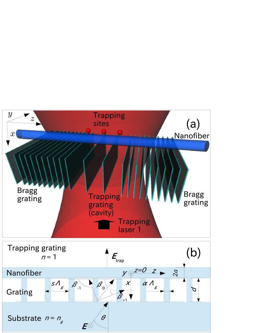
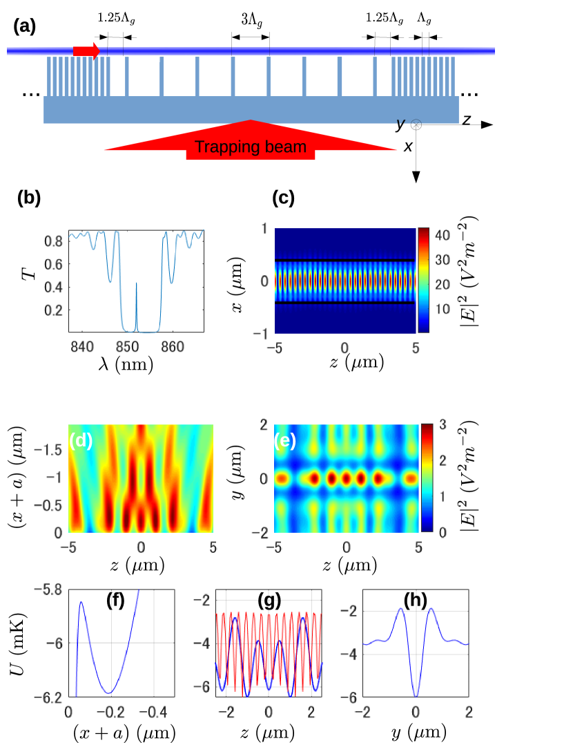
Here we describe a scheme to trap atoms in arrays near to the surface of a composite nanostructure which can potentially solve these problems as well as provide new features compared to the aforementioned studies. The device we consider here is a nanostructure comprised of a nanofiber mounted on a grating. Similar devices have recently been experimentally investigated for the purposes of enhancing the coupling of a quantum emitter to the guided modes of an optical nanofiber OurGrating ; OurPRL ; OurOL . Here, we will show that by illuminating such a device, it is possible to create periodic arrays of trapping potentials near to the nanofiber surface as depicted in Fig. 1(a).
The basic principle of the device is that a longer period grating (referred to here as a trapping grating) between two Bragg gratings on a nanostructured silica substrate can serve the dual purposes of 1) enhancing emission into the integrated nanofiber by acting as a cavity and 2) acting as a first order grating for trapping light which illuminates the device. The principle advantages of the proposed device are as follows: a) An array of traps can be formed along the nanofiber surface, with the number of traps and their period determined by the design of the nano-structured substrate, rather than the wavelength of the trapping light. A major application of this, as we will show later, is trapping devices where the trapping sites are geometrically guaranteed to have their centers aligned to antinodes of a cavity mode of the device. b) Unlike trapping schemes which use the evanescent tails of the guided modes, in our scheme no trapping light is present in the guided mode, which should lead to improved signal-to-noise ratios for detection of photons emitted into the guided mode. c) Unlike trapping arrays formed by the guided modes of the nanofiber, the traps formed by this technique have linear rather than elliptical polarization. This means the potentially decohering effect of vector light shifts KimbleNFNJP ; FamEJPhysD is not present for our device. d) The composite nature of the device has a number of benefits as given in OurOL . Of particular importance in this instance is the separation of the nanowaveguide function and the index modulation function into separate devices. This allows for much greater diffraction efficiencies into the st order compared to what could be achieved with structures patterned directly onto the waveguide, leading to relatively larger trapping depths along the fiber axis.
The paper proceeds in the following way. First we consider the trapping potential formed when a plane wave is incident on the system with an infinitely long trapping grating and no Bragg-grating region, as depicted in Fig. 1(b). This system may be analysed both numerically and using an analytical model which allows a crosscheck of the numerically calculated potential. Having established the validity of our numerics, we then go on to simulate the full device, including the Bragg mirror regions, using FDTD simulations.
II The device
The device is depicted in a to-scale conceptual image in Fig. 1(a) and in schematic form in Fig. 1(b). (Note that the grating substrate is omitted in Fig. 1(a) for clarity). An optical nanofiber of radius is mounted on a nano-structured substrate and illuminated from the grating side (single-illumination configuration) or from both sides (dual-illumination configuration) by a red-detuned laser beam with a vacuum wavelength . The corresponding wave number of the trapping laser is and the trapping laser frequency is , where is the speed of light in the vacuum.
The nano-structured substrate is divided into two regions. To either side of the center, a Bragg grating region is present. The two Bragg gratings, which have period act as mirrors with respect to the fundamental mode of the nanofiber OurGrating . The central region is the trapping grating (shown in Fig. 1(b)) with period for some real number , i.e., the trapping grating is a first order grating relative to the incident trapping light. We characterize the length of the trapping region by counting the number of regions of width . In this paper, is always an odd number. We note that with respect to the Bragg mirrors, the central trapping grating region may be considered to constitute a cavity of total width . This cavity region acts to enhance coupling of spontaneous emission to the fiber guided modes.
In all regions of the nano-structured substrate, the grating slats have depth m and width nm, where is the Bragg grating duty cycle. As shown in Fig. 1(b), light incident on the device at angle is diffracted into the th and st orders at angles and respectively. In the remainder of the paper, we will take implying that the light is normally incident on the grating substrate.
We define our axes so that is always in the middle of the trapping grating region and corresponds to the fiber center as shown in Fig. 1(b). The unit vectors , and are defined to lie along the , and axes respectively.
In the analytical treatment which follows below, we will only consider the case of normally incident, -polarized trapping light which is red-detuned from the atomic resonance. The effect of changing the incident angle, polarization or detuning will be discussed in the discussion section.
III Evaluation of the trapping potential
III.1 Analytical treatment
III.1.1 Field created by illumination of the composite device
By applying the theory of a planewave scattered from a dielectric grating Knop together with scattering theory for a sub-wavelength dimension cylinder BohrenHuffman the field outside the device for the incident -polarized field can be found. A detailed derivation is given in the Appendix. To summarize the theoretical approach: We make the approximation that evanescent orders of the grating may be ignored, thereby truncating the series which gives the output field. We also assume that the field around the nanofiber can be found by taking the field at the output of the grating as the input field to the scattering problem involving the nanofiber .
To find the field around the fiber we need to find the scattered field due to the th and st order plane waves. To apply the standard scattering formalism, we first evaluate the angles where as shown in Fig. 1(b). In the present paper, we will consider only the case where the trapping beam is at normal incidence to the grating, giving . The other angles are given by , where is the Kronecker delta function, is the wavenumber of the component of the diffracted field and is the wavenumber of the component of the diffracted field.
The field for is then given by
| (1) | |||||
where is the field due to the grating in the absence of the nanofiber (See Appendix), is the transmission coefficient of the th diffraction order, and are th order cylindrical harmonics whose coefficients and respectively depend on the incident angles of the transmitted orders of the grating. These coefficients are defined fully in the Appendix, where a brief review of scattering theory for a dielectric cylinder is given for the case considered here.
III.1.2 Dual illumination
In the dual illumination scheme, a second laser illuminates the device from the fiber side. To derive the trapping field in this case, we will assume that the only fields to be considered are those of the second trapping laser itself, and the scattered field caused by the second trapping laser being incident on the nanofiber. That is, we ignore any reflections from the grating or, indeed, any effects due to the grating at all. Because of the low reflectivity of the grating at the wavelength considered here, this approximation is not a bad one. In particular, for the space , the assumption turns out to produce good agreement with FDTD simulation results. The incident field is given by
| (2) |
where is the relative phase between trapping laser 1 and trapping laser 2 which we will assume is adjustable. The scattered field is then
| (3) |
where the sign of in the argument of the spherical harmonics has been flipped to account for the fact that the incident wave is coming from the negative direction, and the terms in are zero due to the normal incidence of the second trapping beam. Finally, we may write the field due to illumination by both trapping beams 1 and 2 as
| (4) |
Note that in what follows, we will use to denote either the trapping potential for single or dual illumination. The meaning of will always be clear from the context in which it is used.
III.1.3 Calculation of the trapping potential
To calculate the trapping potential experienced by 133Cs atoms, we follow closely the formalism of Ref. LeKien1 . The optical trapping potential may be calculated as
| (5) |
where
| (6) |
The index runs over different transitions of cesium that contribute to the trapping potential. For our purposes, we will include the four dominant lines of the atom LeKien1 corresponding to wavelengths nm, nm, nm and nm, where . The transition strengths for these lines are s-1, s-1, s-1 and s-1. The statistical weights of each transition are , , , and the ground state has weight . Finally, we define the linewidths , where denotes a lower level . However for the detuning of the trapping light considered here, the contribution of the terms to are negligible.
For convenience, all of our analytical and simulation results assume an electric field amplitude of 1. We scale the potential to provide trap depth predictions for a given optical power as follows. For simplicity, we use the waist region of a circular Gaussian beam as a reference. We assume a power and a beam waist radius of . Then the peak intensity in the beam is given by . The scaling factor for the optical part of the trapping potential is then , where is the vacuum permittivity.
Next, we consider the contribution of the van der Waals potential at the fiber surface to the trapping potential. Here we will use the simple flat-surface, bulk-medium van der Waals potential experienced by a Cs atom close to a silica surface which is given in mK by
| (7) |
where is measured in m. This flat potential approaches the Van der Waals potential due to a silica fiber when the distance from the fiber surface approaches zero LeKien1 . The van der Waals potential due to the grating is neglected as the trapping potential minima always lie between two grating slats, i.e., nm away from the nearest slat for the parameters used in this paper. This is sufficiently far that the contribution from the grating slats to the van der Waals potential is negligible.
The total trapping potential is the sum of the optical and Van der Waals potentials:
| (8) |
where it is understood that the factor is only necessary to scale the optical potential if the analytical results and/or simulations have used incident fields of unity amplitude.
III.2 Comparison of theory and finite-difference time-domain numerical calculations
We simulated the electromagnetic field in the system shown in Fig. 1(b) for an incident plane wave using the finite difference time domain (FDTD) method (Lumerical Inc.). Here, and throughout the remainder of this paper, we assume an optical power of 250 mW per beam, a beam spot size of 10 m and a trapping light wavelength of 937 nm (the red detuned magic wavelength for 133Cs) in order to calculate the trapping potential generated by the intensity distribution.
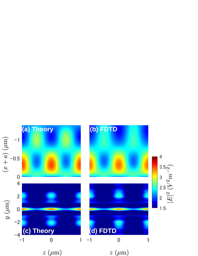
Figure 2 shows a comparison between squared electric field amplitudes as calculated from Eq. 1 and by using FDTD numerical simulations. We see good agreement between the squared field profiles in the plane (Figs. 2(a) and (b)) and the plane (Figs. 2(c) and (d)) both in the qualitative shape of the field pattern and the intensity. In particular, Figs. 2(a) and (b) show the generation of a periodic array of intensity maxima close to the nanofiber surface. Figs. 2 (c) and (d) show that along the axis perpendicular to the fiber, for set to the position of the intensity maximum in the plane, a strong intensity maximum coincides with the center of the fiber. Away from the center is an area of low intensity, and for larger , the diffraction pattern due to the grating is restored since the field scattered by the fiber tends to zero in this region.
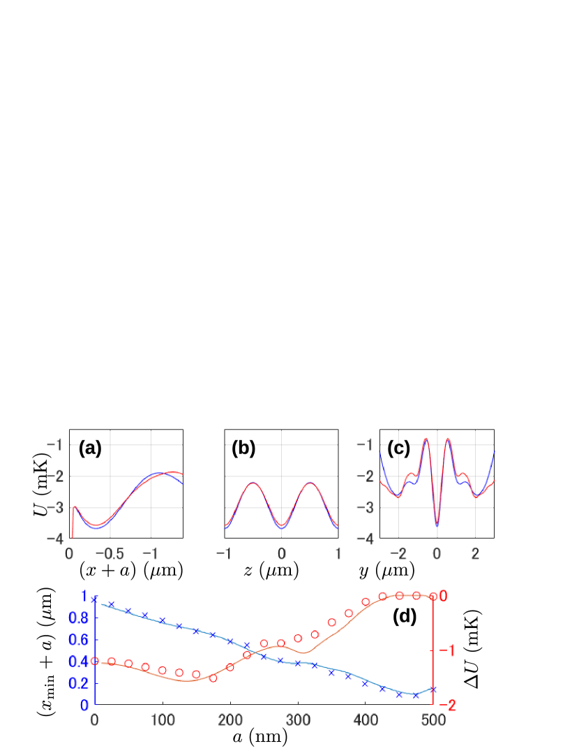
Figures 3(a-c) show the corresponding trapping potential as a function of , and respectively, as calculated from Eq. 8 and from the FDTD data in all cases assuming a power of mW. We see that potential depths of mK order are achievable in all directions for these conditions, although the effect of the Van der Waals potential significantly lowers the potential depth along the -axis. Fig. 3(d) shows how the trapping depth and the trap minimum position on the -axis vary as the fiber radius is varied. It may be seen that increasing the nanofiber radius leads to the trapping potential moving closer to the nanofiber surface, with the trapping potential depth decreasing due to the effect of the Van der Waals potential. It may be seen that for trapping minima positions less that nm the potential depth becomes vanishing.
| Trap freq. | (kHz) | |
|---|---|---|
| Axis | Theory | FDTD |
| 816 | 770 | |
| 1270 | 1320 | |
| 982 | 939 |
In Table 1, we show the trapping frequencies along each axis for the theoretically and FDTD calculated trapping potentials shown in Figs. 3(a-c). In all cases we find fair agreement between theoretically and FDTD calculated values.
We will now show that a dual illumination scheme can produce trapping potentials much closer to the fiber-surface while maintaining potential depths of order K. Because the introduction of the counter-propagating beam principally affects the potential shape along the -axis, we focus on the -dependence of the potential in what follows.
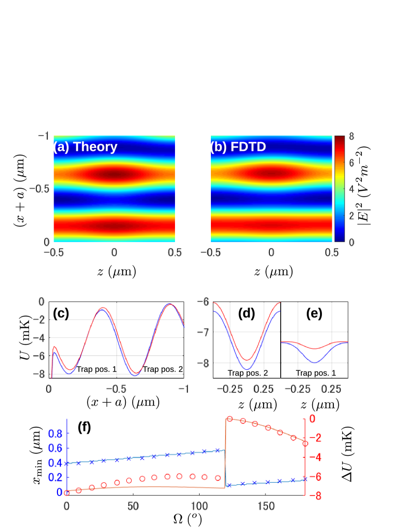
Figure 4 (a) shows the squared electric field amplitude as given by Eq. 4, while the results of FDTD simulations are shown in Fig. 4(b). Unlike the single illumination case, because a standing wave pattern is formed, a number of trapping potentials are formed in the plane. We will focus on the traps which are nearest and next-nearest to the fiber surface as shown in Figs. 4(a,b). Figure 4(c) shows the -dependence of the trapping potential for and a relative phase of between trapping beams 1 and 2. Of note is that the position of the trapping potential minimum closest to the nanofiber surface (Trap pos. 1) is only nm. The -dependent trapping potential at this position has a depth of mK. Additionally, a much deeper trap is found about 600 nm from the fiber surface (Trap pos. 2).
Figures 4 (d) and (e) show the dependence of the trapping potential at the -axis trapping centers furtherest and closest to the fiber surface respectively. As seen in Fig. 4 (e), there is a large difference in the trap depth predicted by the theoretical model and the FDTD data when the trap is close to the fiber surface. This might be due to the presence of evanescent fields from higher order grating modes which are explicitly neglected in our theoretical model. Fig. 4 (e) thus illustrates the limits of the simple model in quantitatively predicting the potential depth along the axis. Figure 4(f) shows the dependence of the trapping potential depth and the position of the trapping minimum as the phase between the two trapping lasers is varied. Up to about , the smaller trapping potential is not separated from the fiber surface and the closest trapping potential is formed by the second intensity maximum at nm from the fiber surface. For phases greater than , the trapping potential closer to the fiber surface becomes distinct and the values of and jump to the new levels associated with this trapping potential as seen in Fig. 4(f). The ability to smoothly control the position and depth of the trapping potential by varying the phase between the two lasers may be useful for loading of the the trapping sites.
| Trap freq. | (kHz) | |||
| Trap | pos. 1 | Trap | pos. 2 | |
| Axis | Theory | FDTD | Theory | FDTD |
| 4100 | 4000 | 4320 | 4270 | |
| 809 | 539 | 1140 | 1100 |
In Table 2, we show the trapping frequencies along the axis for the theoretically and FDTD calculated trapping potentials shown in Figs. 4(c-e) for both trapping position 1 (closest to the nanofiber) and trapping position 2. Results for the axis are also shown for comparison, but as expected, the values are little changed from the single-illumination case, when the trap is sufficiently far from the fiber surface. We find fair agreement between theoretical and FDTD calculated values in all cases, except in the case of the -dependence of the potential closest to the fiber, for reasons noted above.
IV Numerical results for experimentally realistic structures
In the following section, we simulate the trapping potential created by experimentally realistic structures for which the trapping grating is of finite length and a Bragg mirror structure exists to either side of the trapping grating. All parameters are the same as in Section III.2.
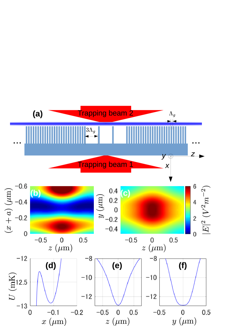
In order that the positions of the traps coincide with antinodes of the cavity mode, a modification to the structure of the device is necessary. We wish to make the cavity mode antinodes appear exactly in the middle of the trapping grating slats so that they coincide with the center of the optical trap. To achieve this, it is necessary that while the trapping grating period is an integer multiple of as before, the overall length of the cavity region should be given by for integer (which is an odd multiple of ). We achieve this condition by adding two shorter grating regions of length at each end of the trapping grating region, as illustrated in Fig. 5(a).
We set for the trapping grating, nanofiber diameter nm, grating period nm, and , giving a trapping grating period of nm. The transmission spectrum through the nanofiber for the fundamental mode is shown in Fig. 5(b). Note that a single cavity mode arises near the middle of the photonic stop band. The associated intensity distribution at the cavity resonance frequency is shown in Fig. 5(c). Typical Q-values for composite cavities such as this device have been measured to be with associated cooperativities (equivalent to the Purcell factor in the regime considered here) of OurPRL .
Figures 5(d) and (e) show the squared field pattern in the and planes respectively and Figs. 5(f-h) show the associated trapping potentials formed along the , and axes respectively. As seen in Fig. 5(f), the trapping potential is formed about 200 nm from the fiber surface and the trap depth along the -axis is K. Although 7 trapping cavities are present, Fig. 5(g) shows that only 5 distinct trapping potentials, with trap depths of mK, are seen along the z axis due to the decreasing intensity of the Gaussian beam away from along with the weaker diffraction pattern at the edge of the trapping grating.
Figure 5(g) also shows the intensity distribution of the cavity mode overlayed as a red line. This figure demonstrates an important property of our deivce: namely that the trapping potential minima can be made to coincide almost perfectly with cavity antinodes by careful design of the grating structure. Indeed, the slight difference between the cavity anti-node positions and the trapping minima positions is mainly due to edge effects of the relatively short trapping grating. We would expect even better coincidence between the trapping sites and cavity antinodes as is increased. Figure 5(h) shows that the trapping potential measured in the direction has the largest trap depth of mK.
The second case we consider is that of trapping a single atom to achieve large coupling efficiency with the nanofiber. We note that is the minimum number of trapping cavities necessary to achieve a trapping minimum in the middle of the trapping cavity. Therefore we choose , and choose a double illumination scheme which can achieve trapping nearer to the nanofiber surface compared with single illumination as discussed in Section III.2.
Figure 6 shows the trapping potential formed by dual illumination in the central trapping region where m for an optical power of 250 mW in each beam. The relative phase between the trapping beams was . Figures. 6(b) and (c) show the squared field pattern in the and planes respectively. As seen in Fig. 6(d), a trapping minimum is formed very close ( nm) to the fiber surface with a trapping depth of about 1 mK. The trapping potential along the -axis is much tighter than in the case of single illumination. Figs. 6(e) and (f) show that the trap depth along the and axes is mK.
| Trap freq. | (kHz) | |
|---|---|---|
| Axis | Single Illum. | Dual Illum. |
| 1180 | 5300 | |
| 1440 | 1460 | |
| 1164 | 1480 |
Table 3 compares the trapping frequencies for FDTD calculated trapping potentials in the cases of single and dual illumination as shown in Figs. 5(e-g) and 6(d-f) respectively. As expected, we find essentially no change along the -axis, and the change along the -axis is small. However the axis value is more than quadrupled due to the tighter trap created by the standing wave as well as the closer proximity of the trap to the fiber surface.
V Discussion and conclusion
We now consider aspects of our system not discussed in the preceding sections. First the question arises as to our choice of parameters for the trapping light. Regarding blue detuned trapping schemes, because the focusing effect of the nanofiber determines the distance of the trapping potential minimum from the fiber surface and the focus is always an intensity maximum, trapping sites tend to be further from the nanofiber in the blue detuned case. We also calculated the potential at the blue-detuned magic wavelength of 686 nm, but we found that red-detuned trapping light produced traps closer to the nanofiber surface.
As for the polarization of the trapping beam, in this work we used exclusively polarized light. This polarization is parallel to the grating slats, so that the output polarization of the grating is also polarized. On the other hand, polarized illumination of the nanofiber produces a field which includes localized polarized components at azimuthal angles of on the fiber surface. Nonetheless, we found that the polarization of the trapping field is also -polarized near the trapping minima to a good approximation, with less than polarization at the trap center, and slightly less than polarized at 300 nm away from the trap center in the direction (corresponding to a temperature of mK). Additionally, we found that illuminating the device with -polarized light did not produce trapping potentials due to the mixture of polarizations resulting after diffraction by the grating.
Next, we note that in the case of non-normal incidence, a diffraction pattern (and thus a trap) is only produced if the incident angle . This is because the gratings considered here are strictly first order gratings. This means that the device must be precisely aligned in order to produce a trapping potential.
Additionally, here we have principally considered the trapping sites closest to the fiber surface. This is justified by the exponential scaling of the coupling between a dipole emitter and the fiber guided mode, atoms trapped in more distant trapping sites have negligible coupling to the nanofiber LukinNWG .
Another issue to consider in the present scheme is the possibility that large light intensities might affect the integrity of the very thin silica slats on the grating. However, the slats are at intensity nodes of the trapping field for the cases considered here. Additionally, the trapping intensity produced by the interference of diffracted orders of the grating is only of order twice the input intensity. For these reasons the thin grating slats are not in general exposed to large field intensities.
Lastly, we consider issues related to the tuning of the cavity. Illumination of the device may cause thermal expansion and thus drifting of the cavity mode from its design wavelength. We note, however, that much of the optical power for circular beam illumination is unused, due to the thinness of the nanofiber. If, for example, we used an elliptical beam with a -axis radius of 10 m as before but an -axis radius of only 1 m, the optical power required to achieve the same intensity at the device surface would be only of that necessary in the case of a circular beam (i.e. mW). In this way heating of the silica substrate would be drastically reduced. If tuning of the cavity resonance is required, it can be achieved by slightly rotating the nanofiber relative to the grating slats (increasing the resonance wavelength) or by lifting the fiber slightly off the grating substrate (reducing the resonance wavelength).
In conclusion, we have analytically and numerically investigated trapping atoms close to the surface of a composite nanooptical device consisting of an optical nanofiber mounted on a grating. Illumination of the device from the grating side produces an array of traps with separations from the nanofiber surface down to 200 nm. Adding illumination from the fiber side can produce trapping potentials within 100 nm of the nanofiber surface. Bragg gratings to either side of the trapping grating create a cavity enhancing the coupling of spontaneous emission into the nanofiber guided modes, and by appropriately designing the grating structure, arrays of atoms may be trapped at positions which correspond to antinodes of the cavity mode. Because optical nanofibers offer automatic coupling to standard fiber optical networks, and due to the advantages of the present scheme over existing nanofiber trapping schemes, we expect that it may be useful in a variety of situations. These include the realization of collectively enhanced scattering into the nanofiber guided modes from an array of atoms, through to quantum information applications where distant atoms must be coupled to the same cavity mode.
MS acknowledges support from a grant-in-aid for scientific research (Grant no. 15K13544) from the Japan Society for the Promotion of Science (JSPS). KPN acknowledges support from a grant-in-aid for scientific research (Grant no. 15H05462) from the Japan Society for the Promotion of Science (JSPS). The authors thank K. Hakuta for his scientific input at the early stages of this research and for his support. We also thank F. Le Kien for discussions regarding the van der Waals potential, M. Morinaga for advice regarding the scattering problem, and R. Yalla for discussions related to the numerical simulations.
Appendix A Numerical simulation protocols
For comparison with theoretical results, we performed FDTD simulations using plane wave sources in our simulations. For scaling the potential, we choose a beam waist radius of m, an optical power of mW, and a wavelength of nm. In the dual illumination case, we assumed beam recycling was possible so that the power in both forward and backward propagating beams was set to . In FDTD simulations of periodic systems using plane waves, care must be taken in interpreting the results since artifacts of the FDTD method can form regular periodic intensity maxima of a similar nature to the true trapping maxima we wish to find. We used periodic boundary conditions for these simulations to ensure that no edge-effects due to the FDTD boundary conditions were present. We also checked that removing all structures in the simulation gave rise to a flat intensity profile, and that removing the grating structure led to the disappearance of all -periodic structures in the output intensity pattern. Once these checks had been passed, we could be confident that any local intensity maxima in the simulations corresponded to the physical nature of the scattered field rather than numerical artifacts. Comparison with the analytical results given in the previous sections also functioned as a further cross-check of our numerical results.
We note that in the case of dual illumination, the relative phase is just the phase of the second beam as set in our FDTD simulations. It is neccesary to match the phase between the theoretical trapping potential and the FDTD calculated trapping potential for a single data set before the FDTD and theory results can be compared for arbitrary phases.
In the simulations for the case of realistic experimental structures, we illuminated the device with a Gaussian beam. We used absorbing rather than periodic boundary conditions, and it was necessary to make the FDTD simulation region large enough that the Gaussian beam tails had decayed effectively to zero by the edges of the simulation region to avoid edge effects such as reflection from the absorbing boundary. However, computer memory limits the mesh density which can be achieved in these large simulation regions. We used linear interpolation to reconstruct the results on a finer grid to improve the detail visible in the Figures. As before, we checked the validity of our simulations by removing all structures from the simulation region and checking that only a Gaussian intensity profile remained in such cases.
Appendix B Field due to a plane wave incident on a dielectric grating
In our analytical derivation of the trapping potential we will use the axes and variables defined in Fig. 1(b). In particular, we assume a grating structure with period , where is the Bragg grating period, is an integer chosen so that the trapping grating is a first order grating. The grating structure has a depth and the grating slats have thickness , where is the duty cycle. The grating is assumed to have refractive index at the trapping light wavelength, and for simplicity the grating structure is assumed to be fabricated on top of a silica substrate which has much larger dimensions than any of the other scales in the problem. (In typical experiments the substrate has been of size 15 mm x 5 mm x 2 mm OurGrating ). The axes are defined as shown in Fig. 1(b) and the unit vectors , , and are aligned with the , , and axes respectively.
A plane wave is assumed to be incident on the structure originating from the direction at an angle as shown in Fig. 1(b) of our manuscript. The grating diffracts the incident wave into th and st orders with angles and respectively. In what follows, standard harmonic time dependence is assumed for all fields and is not explicitly shown.
We first consider the electric field at the output of the grating in the absence of the nanofiber. This problem was solved by Knop in Knop but due to a typographical error, the result given was ambiguous. For clarity, we therefore reproduce the results of Knop below giving the correct fromula which we have checked by rederiving the results. For an incident field
| (9) |
the field outside the grating is given by
| (10) |
where
| (11) |
is the axis wavenumber and
| (12) |
is the axis wavenumber for diffraction order . The coefficients give the (complex) amplitude of each diffracted component.
Although they do not contribute to the trapping potential, we also define the axis wavenumbers of the plane wave components reflected at the grating interface which are given by
| (13) |
Also, note that the phase term , which does not appear in Knop , is necessary to retard the phase of the solution since the grating output is offset from the origin along the -axis by (the output of the grating is at in Knop ).
The coefficients of the different plane wave components are given by
| (14) |
where is a matrix with components
where is a matrix of eigenvectors and are the eigenvalues of the eigenvalue equation
| (16) |
where , and is the th Fourier coefficient of the refractive index profile of the grating Knop . The vector is made up of zeros except for a single element at which has the value
| (17) |
It is well known that the numerical inversion of required to calculate is unstable when significant numbers of evanescent diffraction orders are included in the calculation KnopImprovedNumericsPaper . In this paper, we will only consider first order gratings, i.e. all but the th and th diffraction orders are evanescent. As noted in Knop , a simple way to avoid the problems due to inversion of near-singular matrices is simply to truncate the eigenvalue problem. Therefore we approximate as a length three vector and matrices , and are taken to have size . This means that we neglect all evanescent orders of the grating which is a good approximation when the distance from the grating is more than the wavelength of the trapping light. This approximation is justified by the good agreement it produces when compared to the results of FDTD numerical simulations.
Appendix C Review of the solution for a planewave incident at oblique incidence on a dielectric cylinder
We now review the analytical form of the field created when a plane wave is incident on a dielectric cylinder at oblique incidence with angle . The treatment follows exactly that of Ref. BohrenHuffman and is included here only for convenience, not as a new result of our study. The following results are valid for the case where the propagation vector of the incident wave lies in the plane and the polarization is parallel to the axis.
We first define cylindrical coordinates for our system. The azimuthal coordinate is given by , and the radial coordinate is given by . For the cylindrical unit vectors, we define , the radial unit vector, and , the azimuthal unit vector.
To proceed, we introduce the vector cylindrical harmonics which are given by the following formulae:
| (18) |
| (19) |
where , and is the th order Hankel function. Note that although the arguments to the cylindrical harmonics are given as cartesian coordinates, calculations take place in polar coordinates.
The field scattered by the cylinder can now be written as
| (20) |
where the coefficients and are defined as follows.
| (21) |
| (22) |
The dependent coefficients have the following defintions:
| (23) |
| (24) |
| (25) |
| (26) |
| (27) |
where , and .
Finally, the total field is found by adding the incident field to the scattered field, i.e.
| (28) |
Appendix D Formula for the electric field outside composite device where
We can now write down the formula for the electric field outside the device as used in our manuscript. We will approximate this field by the output field of the grating as scattered by the nanofiber. Noting that and depend on the incident angle , we write and . Then, by applying Eq. 28 along with Eq. 20 for each diffraction order of the grating, we can write the field outside the device in the region for the case of single illumination as
| (29) | |||||
References
- (1) H.J. Kimble, “The quantum internet,” Nature 453, 1023-1030 (2008).
- (2) K.J. Vahala, “Optical microcavities,” Nature 424, 839-346 (2003).
- (3) T. Aoki, B. Dayan, E. Wilcut, W. P. Bowen, A. S. Parkins, T. J. Kippenberg, K. J. Vahala, and H. J. Kimble, “Observation of strong coupling between one atom and a monolithic microresonator,” Nature 442, 671-674 (2006).
- (4) F. Le Kien, V. I. Balykin, and K. Hakuta, “Atom trap and waveguide using a two-color evanescent light field around a subwavelength-diameter optical fiber,” Phys. Rev. A 70, 063403 (2004).
- (5) E. Vetsch, D. Reitz, G. Sagué, R. Schmidt, S. T. Dawkins, and A. Rauschenbeutel, “Optical Interface Created by Laser-Cooled Atoms Trapped in the Evanescent Field Surrounding an Optical Nanofiber,” Phys. Rev. Lett. 104, 203603 (2010).
- (6) A. Goban, K. S. Choi, D. J. Alton, D. Ding, C. Lacroûte, M. Pototschnig, T. Thiele, N. P. Stern, and H. J. Kimble, “Demonstration of a State-Insensitive, Compensated Nanofiber Trap,” Phys. Rev. Lett. 109, 033603 (2012).
- (7) M. Daly, V.G. Truong, C.F. Phelan, K. Deasy and S. Nic Chormaic, “Nanostructured optical nanofibres for atom trapping,” New J. Phys. 16, 053052 (2014).
- (8) J. D. Thompson, T. G. Tiecke, N. P. de Leon, J. Feist, A. V. Akimov, M. Gullans, A. S. Zibrov, V. Vuletic, and M. D. Lukin, “Coupling a single trapped atom to a nanoscale optical cavity,” Science 340 1202-1205 (2013).
- (9) C.-L, Hung, S.M. Meenehan, D.E. Chang, O. Painter, and H.J. Kimble, “Trapped atoms in one-dimensional photonic crystals,” New J. Phys 15, 083026 (2013).
- (10) S. Kato,, and T. Aoki, “Strong Coupling between a Trapped Single Atom and an All-Fiber Cavity,” Phys. Rev. Lett. 115, 093603 (2015).
- (11) K. J. Arnold, M. P. Baden, and M. D. Barrett, “Self-Organization Threshold Scaling for Thermal Atoms Coupled to a Cavity,” Phys. Rev. Lett. 109, 153002 (2012).
- (12) J. Lee, G. Vrijsen, I. Teper, O. Hosten, and M.A. Kasevich, “Many-atom–cavity QED system with homogeneous atom–cavity coupling,” Opt. Lett. 39, 4005-4008 (2014).
- (13) O. Hosten, N.J. Engelsen, R. Krishnakumar, and Mark A. Kasevich, “Measurement noise 100 times lower than the quantum-projection limit using entangled atoms,” Nature 529, 505-508 (2015).
- (14) F. Le Kien, P. Schneewies, and A. Rauschenbeutel, “Dynamical polarizability of atoms in arbitrary light fields: general theory and application to cesium,” Eur. Phys. J. D 67, 92 (2013).
- (15) F. Le Kien, S. Dutta Gupta, K. P. Nayak, and K. Hakuta, “Nanofiber-mediated radiative transfer between two distant atoms,” Phys. Rev. A 72, 063815 (2005).
- (16) M. Sadgrove, R. Yalla, K. P. Nayak, and K. Hakuta, “Photonic crystal nanofiber using an external grating,” Opt. Lett. 38, 2542-2545 (2013).
- (17) R. Yalla, M. Sadgrove, K. P. Nayak, and K. Hakuta, “Cavity Quantum Electrodynamics on a Nanofiber Using a Composite Photonic Crystal Cavity,” Phys. Rev. Lett. 113, 143601 (2014).
- (18) J. Keloth, M. Sadgrove, R. Yalla, and K. Hakuta, “Diameter measurement of optical nanofibers using a composite photonic crystal cavity,” Opt. Lett., 40, 4122-4125 (2015).
- (19) C. Lacroute, K.S. Choi, A. Goban, D.J. Alton, D. Ding, N.P. Stern, and H.J. Kimble, “A state-insensitive, compensated nanofiber trap,” New J. Phys. 14, 023056 (2012).
- (20) K. Knop, J. Opt. Soc. Am. 68, 1206 (1978).
- (21) C. F. Bohren and D. R. Huffman, “Absorption and Scattering of Light by Small Particles”, Wiley-VCH (2004).
- (22) M. G. Moharam, Eric B. Grann, and Drew A. Pommet, J. Opt. Soc. Am. 12, 1068 (1995).