Quantum transport through MoS2 constrictions defined by photodoping
Abstract
We present a device scheme to explore mesoscopic transport through molybdenum disulfide (MoS2) constrictions using photodoping. The devices are based on van-der-Waals heterostructures where few-layer MoS2 flakes are partially encapsulated by hexagonal boron nitride (hBN) and covered by a few-layer graphene flake to fabricate electrical contacts. Since the as-fabricated devices are insulating at low temperatures, we use photo-induced remote doping in the hBN substrate to create free charge carriers in the MoS2 layer. On top of the device, we place additional metal structures, which define the shape of the constriction and act as shadow masks during photodoping of the underlying MoS2/hBN heterostructure. Low temperature two- and four-terminal transport measurements show evidence of quantum confinement effects.
I Introduction
Van-der-Waals heterostructures based on graphene and transition metal dichalcogenides (TMDCs) are attracting increasing attention in mesoscopic physics and solid-state researchNovo16 ; Geim13 ; Rad10 ; Herr13 ; Rus08 ; Ter16 . One of the main challenges in this field is to find ways of confining charge carriers in well defined device geometries. Achieving a high degree of control over carrier confinement is necessary for manipulating individual charges or spinsElz04 ; Wee88 ; Wep13 ; Joh92 , as well as for investigating mesoscopic physics phenomena such as quantized conductance or valley filtering in bilayer graphene and TMDCs Ryc07 ; Piso17 . Moreover, good control over carrier confinement is a necessary requirement for studying fundamental material properties such as the Landé g-factor and the charge carrier’s effective mass in mesoscopic devices.
Because of the absence of a band gap, mesoscopic physics in graphene is mostly studied in devices where the material has been etched into the desired shapeTer16 ; Rus08 . These devices typically suffer from scattering and trap states on their rough edgesTer16 ; Tom11 ; Bis14 . In contrast, bilayer grapheneGos12 ; All12 and semiconducting TMDCsSon15 ; Ke16 allow for soft electrostatic confinement with the help of metallic gates, similarly to what has been pioneered in two-dimensional electron gases (2DEGs) in conventional semiconductor heterostructures for the past decadesWee88 ; Gold1998 ; Petta05 . First experiments on confining charge carriers in MoS2 and forming one-dimensional transport channels by electrostatic gating have recently been performed KLee16 ; Ke16 ; Piso17 ; ZZZhang17 ; CHSharma17 ; SBhandari17 . Here, we demonstrate an interesting method of defining arbitrary doping profiles in van-der-Waals heterostructures based on few-layer (two to five layers) MoS2 encapsulated in hexagonal boron nitride (hBN). In analogy to remote doping in semiconductor 2DEGs, we make use of the photodoping effect recently observed in hBN/graphene heterostructuresJu14 ; Wong15 ; Neu16 . We use this effect to define stable and smooth sub-wavelength lateral doping profiles in MoS2 employing metal shadow masks that are lithographically defined on top of an hBN/MoS2/hBN heterostructure. Our photo-induced remote doping approach enables us to reach free charge carrier densities of up to cm-2, when using an additional gate voltage during light illumination. It thus allows to create arbitrary carrier density profiles defined by the shadow mask geometry. The feasibility of our approach is demonstrated by studying quantum transport through constrictions in MoS2. We expect that our method allows to fabricate more complex geometries such as antidot lattices or Aharonov-Bohm rings with the advantage that the metal used for shadow masking does not need to be electrically contacted, when studying mesoscopic transport.
II Sample fabrication
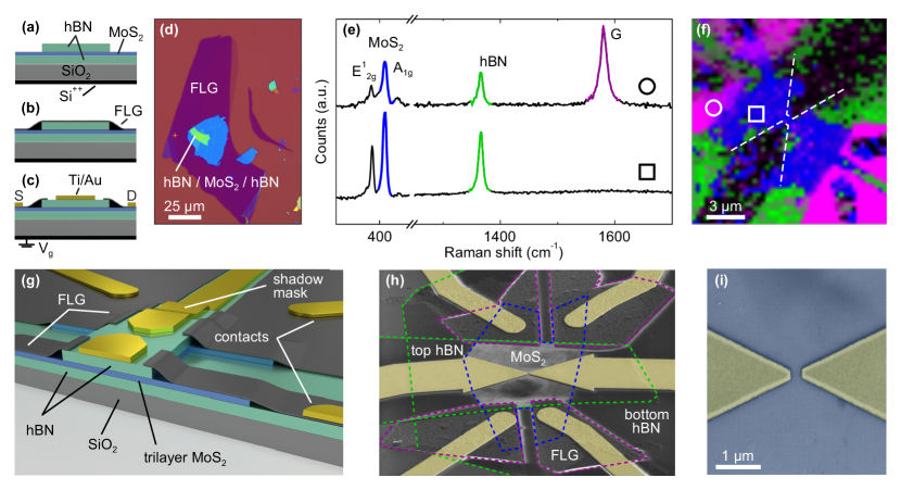
All samples are fabricated using the well-established dry delamination van-der-Waals stacking techniqueWan13 ; Bansz15 . A few-layer MoS2 crystal gets partially encapsulated between two hBN flakes and is then placed onto a Si++/SiO2 substrate (Figure 1a), where the highly doped Si++ substrate is used as a global back gate. In order to electrically contact the MoS2 from the top surface, the left and the right parts of the MoS2 flake remain uncovered by the upper hBN crystal. At the same time, the inner fully encapsulated area of MoS2 is well protected against transfer related degradation and contamination ensuring a high quality of the device. Thereafter, one large flake of few-layer graphene (FLG) is placed on top of the entire structure, which is in direct contact with MoS2 in all parts that are not protected by the upper hBN flake (Figure 1b). Figure 1d shows an optical microscopy image of such a complete van-der-Waals stack. In contrast to previous reportsRoy14 ; Yu14 ; Cui15 , where multiple flakes of FLG have been transferred to fabricate electrical contacts, we only transfer a single large FLG flake that is subsequently patterned (Figure 1c). Using a single flake to contact multi-terminal MoS2 devices is convenient, as it saves several transfer steps or crystal phase engineering of the MoS2Kap14 . Furthermore, it prevents any direct contact of solvents or wet chemistry with the MoS2. Only after the last transfer step, we immerse the sample in solvents, where also the outer parts of the MoS2 are already fully encapsulated by the FLG. Electron-beam lithography and reactive ion etching (RIE) using an Ar/O2 plasma with a flux of 32 sccm Ar and 8 sccm O2 and a power of 60 W allow to selectively etch the FLG and the MoS2, while the etching rate is negligible for the top hBN. This enables us (i) to remove the FLG covering the top hBN and (ii) to etch trenches through the FLG/MoS2 heterostructure. The trenches are needed to separate the individual leads on each side of the multi-terminal devices (see illustration in Figure 1g). In a last step, Ti/Au contacts (typical thickness of 5/95 nm) to the FLG, as well as the shadow mask structures for the constriction on the top hBN (see also Figure 1c) are evaporated, followed by lift-off.
The devices are characterized by scanning confocal Raman microscopyGraf07 which enables us to spatially probe the structural (and partly electronic) quality of all individual layers of the van-der-Waals heterostructure. Additionally, we follow ref. 35 to determine the number of layers of the MoS2 from these Raman spectra. Figure 1e depicts two typical Raman spectra for a trilayer MoS2 constriction device. The upper spectrum in Figure 1e is recorded in the lead area (see open circle in Figure 1f), where the MoS2 is covered with FLG. The G peak at 1583 cm-1 (purple) originates from the FLGDressel09 . The hBN peak is located at around 1365 cm-1 (green)Gor11 while the A1g and the E modes of the trilayer MoS2 are located around 409 cm-1 (blue) and 386 cm-1, respectivelySah13 ; Ton13 . The lower spectrum in Figure 1e is recorded on the hBN/MoS2/hBN area of the device, close to the shadow masks, where only the two peaks from the hBN and the MoS2 are visible (see open square in Figure 1f). Figure 1f shows a Raman map of the intensities of the characteristic Raman peaks of the 2D materials in use. Green represents the intensity of the hBN peak, purple depicts the G-peak intensity of the FLG, blue shows the intensity of the A1g mode of the MoS2. The dark areas are the gold shadow masks, which define the constriction in the underlying MoS2 layer. Figure 1h shows a false color scanning electron microscopy image (SEM) of a typical device. The boundaries of the individual flakes are indicated by the dashed colored lines, where we use the same color code as in Figure 1e. Figure 1i shows a close up SEM image of a typical shadow mask structure with a width of 250 nm and a length of 175 nm.
III Results and discussion
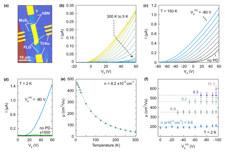
We start by discussing charge transport in a trilayer MoS2 Hall bar structure and explore the method of photodoping before discussing transport through the MoS2 constrictions. The Hall bar device (see Figure 2a) was fabricated the same way as described above. In Figure 2b we show the current flowing through the Hall bar, which is measured in standard four-terminal geometry in longitudinal configuration as function of the applied gate voltage for temperatures ranging between 300 K to 5 K at a constant bias voltage of Vb = 100 mV. Prior to photodoping (PD), the overall current strongly decreases with decreasing temperature and falls below our detection limit for temperatures less than 10 K (see corresponding green curve taken at 2 K in Figure 2d). The strong decrease of current at low temperatures is due to (i) a strong increase of the MoS2 resistance and partially (ii) to an increase of the contact resistance (see supplementary materials, Figures S1a and S1b). The increase in resistivity of the MoS2 is most likely due to localization effects. At higher temperatures, we observe a gate dependent insulator-to-metal transition identified by the onset of the current flow in Figure 2b, which continuously shifts to smaller gate voltages with increasing temperature. Similar observations of a charge carrier density dependent insulator-to-metal transition in MoS2 have been recently reportedRad13 ; Bau13 ; Sch14 . Metallic conductance at low temperatures can be observed for high charge carrier densities around cm-2. In order to adjust the charge carrier density in our devices we make use of the recently reported photodoping mechanism across a hBN-to-graphene interfaceJu14 ; Wong15 ; Neu16 . Nitrogen vacancies and/or carbon impurities in the hBN crystal can be optically activated and act as a charge reservoir. By illuminating our hBN/MoS2/hBN Hall bar using a high energy light emitting diode (LED) with a center wavelength of 470 nm, these hBN defect states get optically excited. By applying a gate voltage, the activated charges are transferred into the MoS2 layer leaving behind oppositely charged states in the hBN layer. The charge transfer continues until the applied (back gate induced) electric field gets fully screened by the charged hBN layer. When turning off the LED, the charges become trapped in the hBN resulting in a constant carrier doping of the illuminated area of MoS2. In agreement with earlier work on similar photodoping of grapheneJu14 ; Neu16 , we observe that the doping is stable over the entire measurement period (up to several weeks) in the temperature range between 2 K and 250 K. All transport measurements have been performed after the LED has been switched off. As any excitation of charge carriers due to the illumination and their relaxation happens in MoS2 on the order of ps to ns Shi2013 ; Palummo2015 we consider the effect of the illumination only to be relevant for the photodoping process.
In a control experiment, where a five-layer MoS2 flake is resting directly on SiO2, (see supplementary materials Figure S3) we observe a volatile and non-systematic photodoping effect, which is either related to the charge traps in the silicon oxide layer or at the SiO2/graphene interfaceDuckKim13 ; Yurg13 . In contrast to the photodoping on hBN, the net doping shift is strongly dependent on the time of illumination and not so much on the applied back gate voltage. Increasing the voltage mainly leads to an increased efficiency, i.e. increased speed, of the doping process consistent with previous studies for photodoping of graphene on SiO2DuckKim13 . Importantly, the induced doping is volatile, i.e. not stable over time and decays directly after switching off the LED.
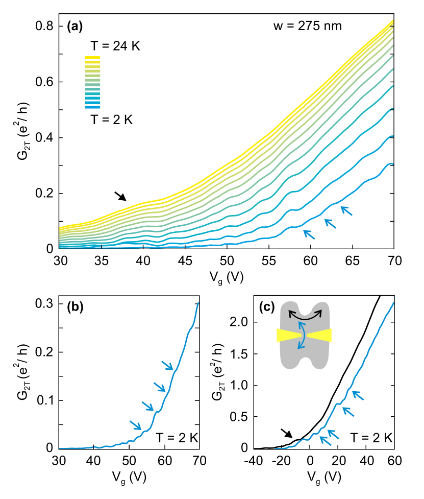
Figure 2c shows a series of gate characteristics of the trilayer Hall bar at 150 K before and after photodoping. The device was illuminated (photodoped) for 10 minutes at constant gate voltages V varying between V V and V V in steps of V V. The illumination time is chosen in such a way that the the photodoping process is saturated. The gate characteristics show a respective overall increase in current, which corresponds well to shifts of V V in gate voltage. At the same time the gate characteristics remain identical in slope and shape indicating a constant charge carrier mobility and a homogeneous and efficient doping process throughout the entire device. After illuminating the Hall bar at V V, the device shows metallic behavior, i.e. it remains well conductive at 2 K when applying moderate gate voltages (see Figure 2d and supplementary materials Figure S2). Charge carrier mobilities extracted from Hall measurements on a typical five layer Mo Hall bar device show values on the order of = 600 cm2/(Vs) at low temperatures (2 K), which decreases to a value of around 45 cm2/(Vs) at room temperature most likely due to electron-phonon scatteringRad13 (see Figure 2e). In the Figure 2f, the extracted charge carrier mobility at 2 K is plotted for different photodoping steps. For each photodoping step the device is warmed up to 150 K (as the LED is freezing out at low temperatures), the photodoping is performed and the device is cooled down again to 2 K to extract the low temperature carrier mobility. The different colors represent different charge carrier densities. The photodoping significantly increase the available range of charge carrier density as in the non-photodoped device was limited to 5.61012 cm-2 when applying reasonable gate voltages. Similar to remote doping in 2DEGsDing1978 , the mobility of the device is not affected by the process of photodoping, as the charge that is introduced in the hBN flake is spatially separated from the MoS2 (see colored dashed lines in Figure 2f). Additionally, we do not observe any significant change of at a fixed gate voltage with respect to the temperature after the photodpoing up to T=150 K. In order to underline the high electronic quality of the heterostructures, we also measure the quantum Hall effect in the five layer MoS2 Hall barCui15 , where we extract quantum mobilities on the order of 2,000 cm2/(Vs) (see supplementary material Figure S3).
Next we discuss constriction devices. For observing size-quantization effects, including quantized conductance, the Fermi wavelength of the carriers has to be on the order of the constriction width. For reasonable carrier densities this requires devices with feature sizes on the order of 100 nm (or below). In order to harness photodoping for such small device feature sizes, we employ a shadow masking technique using non-transparent metal structures. Notably, this approach is in contrast to previous work, where some of us demonstrated photodoping in graphene/hBN heterostructures with micron-scale spatial resolution using a confocal laser set-upNeu16 . The metallic shadow masks, predefined by electron beam lithography, allow to define long-lasting doping profiles in arbitrary geometries (see e.g. Figures 1g-1i). Using this shadow masking technique, we illuminate only the source and drain contact areas (leads) and the constriction, while everything covered by the metal masks is unaffected by the photodoping process. As the MoS2 is non-conductive at 2 K prior to the photodoping no depletion is necessary to form a constriction between the metallic shadow masks. In contrast to conventional constrictions in 2DEGs, we neither have to etch our sample nor have to use electrostatic gates to define the structure as free carriers are only available in the regions, where the sample has been photodoped. In the following, the metallic shadow mask is only used to define the constriction by the photodoping. The devices are only tuned by applying a gate voltage Vg to the highly doped Si++ back gate.
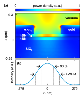
In order to estimate the expected width of the constriction we perform numerical simulations111The simulation was performed using the COMSOL Multiphysics package and assumes vertical illumination of the sample. of the (lateral) light intensity profile responsible for forming the constriction during photodoping. Figure 3 shows the simulated intensity distribution in the constriction region defined by a 275 nm spaced shadow mask. The simulation indicates that the light intensity underneath the shadow mask is strongly suppressed, with a lateral extend of the intensity profile at full-width-at-half-maximum (FWHM) of 240 nm (see arrows in Figure 3b). It has to be emphasized that this value can only be regarded as an upper limit as we do not know (i) the intensity at which photodoping becomes efficient, (ii) to which extend electrostatic effects from the metallic shadow mask and (iii) additional plasmonic effects between the shadow masks may affect the potential landscape in the constriction region. When assuming 90% of the light intensity is needed to form the constriction its width would reduce to around 120 nm or below. To further investigate the influence of these effects, additional experiments are necessary which are beyond the scope of this work. Similar simulations have been performed for different constriction width showing similar results.
Figure 4a shows the two-terminal conductance through a 275 nm wide constriction fabricated from a bilayer MoS2 flake at constant bias of Vb = 3 mV for temperatures ranging from 2 K to 24 K (after photodoping the device at 50 K and V V). The conductance trace at 2 K shows step-like features suggesting confinement effects in the constriction (see Figure 4b). A very similar behavior is observed for all five measured constriction devices (see supplementary Figure S5). The step-like features in the conductance traces remain visible up to 15 K (Figure 2a) with increasing two-terminal conductance. The increasing conductance with a fixed position of the features with respect to Vg could well be a sign of increasing transmission through the constriction until the confinement gets destroyed when the MoS2 underneath the metallic shadow masks starts to contribute to the transport.
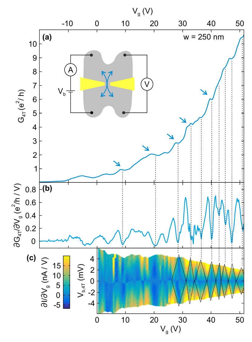
In order to verify that the conductance steps originate from the constriction, we perform two-terminal measurements in different contact configurations on a separate multi-terminal device fabricated from a trilayer MoS2 flake (see Figure 4c) with a constriction width of 250 nm. The black trace in Figure 4c shows the conductance between two contacts on one lead, i.e. on one side of the constriction of a four-terminal device, (see the black arrows in the inset of Figure 4c). The measurements were performed at 2 K after photodoping the device at V V and 50 K. The trace shows a smooth and monotonic increase of the conductance with the applied gate voltage except for a feature close to the onset of the conductance at around V V (see black arrows) and is overall very similar in shape to the traces obtained from several Hall bar devices. The feature close to the transport onset is most likely related to localized states due to the random potential variations from trapped chargesGhat11 . In contrast, the conductance through the constriction (blue trace in Figure 4c) shows the similar extended step-like features as they were observed for the two-terminal device.
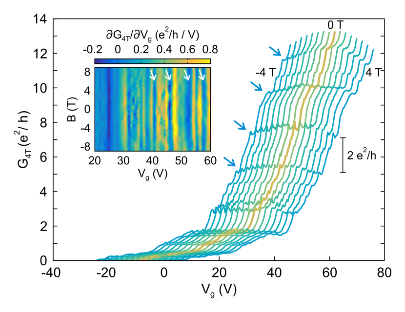
The total resistance from the two-terminal data shown in Figure 4 heavily depends on the particular device. It ranges between 10 and 100 k and is thus significantly larger than the conductance quantum, as the contact resistances heavily contributes to the overall resistance. A subtraction of these parasitic resistances proves difficult as both are strongly gate voltage and bias dependent. In order to reduce the influence of these additional device resistances on the measurement, we performed four-terminal measurements on the multi-terminal trilayer MoS2 device (see inset of Figure 5a). It is important to point out that this four-terminal measurement allows to extract an effective two-terminal conductance as the voltage is probed roughly 4 away from the constriction. This length is significantly larger than the elastic mean free path in the MoS2 2DEG. In Figure 5a we show the four-terminal conductance in unit of the conductance quantum as a function of the applied gate voltage measured at 2 K. The conductance ranges from 0 to 11 and exhibits step-like features which are roughly spaced by 1 to 2 (see blue arrows). This observation is in contrast to the expected appearance of steps at multiples of 6 for a narrow constriction in trilayer MoS2 due to the six-fold degeneracy of the three and three valleys, which govern the transportZWu16 ; Piso17 . However, it is in reasonable agreement with recent measurements performed on a gate-defined nanoconstriction in a MoS2-based heterostructurePiso17 . It might be explained by lifting of the level degeneracies due to the additional confinement of the constriction and/or a reduced transmission through the constriction while we cannot completely exclude that the FLG/MoS2 interface and the MoS2 regions leading to the constriction cause an additional series resistance. The reduced transmission would also explain (i) that the observed step sizes do not meet precisely multiples of 1 or 2 and (ii) the substructure observed on the gate voltage derivative of (Figure 5b) and the bias-dependent measurements (Figure 5c). The latter exhibit well developed diamond-like features for high gate voltages ( V) from which we extract an energy scale of around 3 to 4 meV for the involved subband spacings, where the degeneracy is potentially lifted. At lower carrier density (smaller gate voltages) the bias spectroscopy measurements show signatures of intersecting diamonds, which we attribute to localized states forming in the narrow constriction. In Figure 6 we show the four-terminal conductance as function of gate voltage for different perpendicular magnetic fields ranging from to T. These measurements have been taken on the same device shown in Figure 5 but at a different cool-down. The traces are offset by V V for clarity. We again observe well-developed step-like features with a step height on the order of 1 or 2 (see e.g. the step from to 7 at 4 T). Most importantly, we observe that the step-like features are virtually not tuned by the applied -field. This, on one hand, rules out universal conductance fluctuations as a possible explanation for the observed step- and kink-like features in our measurements. On the other hand, it provides strong indication that the formed constriction is rather narrow such that orbital effects are not playing an important role. The inset in Figure 6 shows the transconductance dG4T/dVg as function of Vg and -field highlighting that the step-like features are indeed not shifting much with -field. We do not know why the experimental data show this weak dependence and why the step-like features only qualitatively match quantized conductance. Further improvement of the device, i.e. MoS2-material quality is needed for more detailed studies on quantized conductance steps in MoS2 or related TMDC materials.
IV Conclusion
In summary, we present a technique to fabricate mesoscopic devices based on MoS2 encapsulated by hBN using an entirely dry transfer process, contacting the MoS2 using few-layer graphene and adjusting the charge carrier concentration using photodoping. By transferring only a single FLG flake to fabricate a large number of contacts to the MoS2, we reduced the complexity of the required van-der-Waals heterostructure significantly. Similar to remote doping in 2DEGs, we are able to adjust the doping level in MoS2, while preserving the charge carrier mobility, resulting in metallic transport at low temperatures. By using metal shadow masks combined with photodoping, we demonstrate a way to produce complex doping profiles on a scale close to the diffraction limit, allowing to observe quantum transport in MoS2 constrictions. In low temperature transport measurements, we reproducibly observe signatures of quantum confinement effects in MoS2 constrictions. Even though gaining precise control over the exact confinement potential proves still to be difficult, our simulations and measurements show that the shadow masking technique can prove useful to generate smooth and long-lasting doping profiles in van-der-Waals heterostructures although most likely the lateral size of structures induced by photodoping is limited by the diffraction limit. This technique could pave the way towards the fabrication of more complex mesoscopic devices in TMDCs, such as for example Aharonov-Bohm rings or antidot lattices, which are difficult to realize using electrostatic gating.
V Acknowledgement
The authors thank F. Haupt for fruitful discussions and S. Staacks for help with the figures. Support by the Helmholtz Nano Facility (HNF)HNF17 , the DFG (SPP-1459), the ERC (GA-Nr. 280140), and the European Union’s Horizon 2020 research program under grant agreement No. 696656 (Graphene Flagship) are gratefully acknowledged. Growth of hexagonal boron nitride crystals was supported by the Elemental Strategy Initiative conducted by the MEXT, Japan and JSPS KAKENHI Grant Numbers JP26248061, JP15K21722 and JP25106006.
References
- (1) K. S. Novoselov, A. Mishchenko, A. Carvalho, A. H. Castro Neto, 2D materials and van der Waals heterostructures. Science 2016, 353, 6298.
- (2) A. K. Geim and I. V. Grigorieva, Van der Waals heterostructures. Nature 2013, 499, 419-425.
- (3) B. Radisavljevic, A. Radenovic, J. Brivio, V. Giacometti and A. Kis, Single-layer MoS2 transistors. Nat. Nanotechnol. 2011, 6 , 147-150.
- (4) B. W. H. Baugher, H. O. H. Churchill, Y. Yang and P. Jarillo-Herrero, Intrinsic Electronic Transport Properties of High-Quality Monolayer and Bilayer MoS2. Nano Lett. 2013, 13, 4212-4216.
- (5) S. Russo, J. B. Oostinga, D. Wehenkel, H. B. Heersche, S. S. Sobhani, L. M. Vandersypen, A. F. Morpurgo, Observation of Aharonov-Bohm conductance oscillations in a graphene ring. Phys. Rev. B 2008, 77, 085413.
- (6) B. Terrés, L. A. Chizhova, F. Libisch, J. Peiro, D. Jörger, S. Engels, A. Girschik, K. Watanabe, T. Taniguchi, S. V. Rotkin, J. Burgdörfer and C. Stampfer, Size quantization of Dirac fermions in graphene constrictions. Nat. Commun. 2016, 7, 11528.
- (7) J. M. Elzerman, R. Hanson, L. W. Van Beveren, B. Witkamp, L. M. K. Vandersypen and L. P. Kouwenhoven, Single-shot read-out of an individual electron spin in a quantum dot. Nature 2004, 430, 431-435.
- (8) B. J. van Wees, H. van Houten, C. W. J. Beenakker, J. G. Williamson, L. P. Kouwenhoven, D. van der Marel and C. T. Foxon, Quantized conductance of point contacts in a two dimensional electron gas. Phys. Rev. Lett. 1988, 60, 848.
- (9) I. van Weperen, S. R. Plissard, E. P. A. M. Bakkers, S. M. Frolov, and L. P. Kouwenhoven, Quantized conductance in an InSb nanowire. Nano Lett. 2013, 13, 387-391.
- (10) A. T. Johnson, L. P. Kouwenhoven, W. De Jong, N. C. Van der Vaart, C. J. P. M. Harmans, and C. T. Foxon, Zero-dimensional states and single electron charging in quantum dots. Phys. Rev. Lett. 1992, 69, 1592-1596.
- (11) A. Rycerz, J. Tworzydlo and C. W. J. Beenakker, Valley filter and valley valve in graphene. Nat. Phys. 2007, 3, 172-175.
- (12) R. Pisoni, Y. Lee, H. Overweg, M. Eich, P. Simonet, K. Watanabe, T. Taniguchi, R. Gorbachev, T. Ihn, and K. Ensslin, Gate-Defined One-Dimensional Channel and Broken Symmetry States in MoS2 van der Waals Heterostructures. Nano Lett. 2017, 17, 5008-5011.
- (13) S. Bhandari, K. Wang, K. Watanabe, T. Taniguchi, P. Kim, and R. M. Westervelt, Imaging Electron Motion in a Few Layer MoS2 Device. J. Phys.: Conf. Ser. 2017, 864, 012031.
- (14) N. Tombros, A. Veligura, J. Junesch, M. H. D. Guimaraes, I. J. Vera Marun, H. T. Jonkman, and B. J. van Wees, Quantized conductance of a suspended graphene nanoconstriction. Nat. Phys. 2011, 7, 697-700.
- (15) D. Bischoff, F. Libisch, J. Burgdörfer, T. Ihn, and K. Ensslin, Characterizing wave functions in graphene nanodevices: Electronic transport through ultrashort graphene constrictions on a boron nitride substrate. Phys. Rev. B 2014, 90, 115405.
- (16) A. M. Goossens, S. C. M. Driessen, T. A. Baart, K. Watanabe, T. Taniguchi, and L. M. K. Vandersypen, Gate-Defined Confinement in Bilayer Graphene-Hexagonal Boron Nitride Hybrid Devices. Nano Lett. 2012, 12, 4656-4660.
- (17) M. T. Allen, J. Martin, and A. Yacoby, Gate-defined quantum confinement in suspended bilayer graphene. Nat. Commun. 2012, 3, 934.
- (18) X.-X. Song, D. Liu, V. Mosallanejad, J. You, T.-Y. Han, D.-T. Chen, H.-O. Li, G. Cao, M. Xiao, G.-C. Guo, and G.-P. Guo, A gate defined quantum dot on the two-dimensional transition metal dichalcogenide semiconductor WSe2. Nanoscale 2015, 7, 16867-16873.
- (19) K. Wang, K. De Greve, L. A. Jauregui, A. Sushko, A. High, Y. Zhou, G. Scuri, T. Taniguchi, K. Watanabe, M. D. Lukin, H. Park, and P. Kim, Electrical Control of Charged Carriers and Excitons in Atomically Thin Materials. Nat. Nanotechnol. 2018, 13, 128-132.
- (20) D. Goldhaber-Gordon, Hadas Shtrikman, D. Mahalu, D. Abusch-Magder, U. Meirav, and M. A. Kastner, Kondo effect in a single-electron transistor. Nature 1998, 391, 156.
- (21) J. R. Petta, A. C. Johnson, J. M. Taylor, E. A. Laird, A. Yacoby, M. D. Lukin, C. M. Marcus, M. P. Hanson, and A. C. Gossard Coherent manipulation of coupled electron spins in semiconductor quantum dots. Science 2005, 309, 2180.
- (22) K. Lee, G. Kulkarni, and Z. Zhong, Coulomb blockade in monolayer MoS2 single electron transistor. Nanoscale 2016, 8, 7755-7760 .
- (23) Z.-Z. Zhang, X.-X. Song, G. Luo, G.-W. Deng, V. Mosallanejad, T. Taniguchi, K. Watanabe, H.-O. Li, G. Cao, G.-C. Guo, F. Nori, and G.-P. Guo, Electrotunable artificial molecules based on van der Waals heterostructures. Sci. Adv. 2017, 3, e1701699.
- (24) C. H. Sharma and M. Thalakulam, Split-gated point-contact for electrostatic confinement of transport in MoS2/h-BN hybrid structures. Sci. Rep. 2017, 7, 735.
- (25) L. Ju, J. Velasco Jr, E. Huang, S. Kahn, C. Nosiglia, H.-Z. Tsai, W. Yang, T. Taniguchi, K. Watanabe, Y. Zhang, G. Zhang, M. Crommie, A. Zettl, and F. Wang, Photoinduced Doping in Heterostructures of Graphene and Boron Nitride. Nat. Nanotechnol. 2014, 9, 348-352.
- (26) D. Wong, J. Velasco Jr, L. Ju, J. Lee, S. Kahn, H.-Z. Tsai, C. Germany, T. Taniguchi, K. Watanabe, A. Zettl, F. Wang, and M. F. Crommie, Characterization and manipulation of individual defects in insulating hexagonal boron nitride using scanning tunnelling microscopy. Nat. Nanotechnol. 2015, 10, 949-953.
- (27) C. Neumann, L. Rizzi, S. Reichardt, B. Terres, T. Khodkov, K. Watanabe, T. Taniguchi, B. Beschoten, and C. Stampfer, Spatial control of laser-induced doping profiles in graphene on hexagonal boron nitride. ACS Appl. Mater. Interfaces 2016, 8, 9377-9383.
- (28) L. Wang, I. Meric, P. Y. Huang, Q. Gao, Y. Gao, H. Tran, T. Taniguchi, K. Watanabe, L. M. Campos, D. A. Muller, J. Guo, P. Kim, J. Hone, K. L. Shepard, and C. R. Dean, One-Dimensional Electrical Contact to a Two-Dimensional Material. Science 2013, 342, 614-617.
- (29) L. Banszerus, M. Schmitz, S. Engels, J. Dauber, M. Oellers, F. Haupt, K. Watanabe, T. Taniguchi, B. Beschoten and C. Stampfer, Ultrahigh-mobility graphene devices from chemical vapor deposition on reusable coper. Sci. Adv 2015, 1, e1500222.
- (30) L. Yu, Y.-H. Lee, X. Ling, E. J. G. Santos, Y. C. Shin, Y. Lin, M. Dubey, E. Kaxiras, J. Kong, H. Wang, and T. Palacios, Graphene/MoS2 hybrid technology for large-scale two-dimensional electronics. Nano Lett. 2014, 14, 3055-3063.
- (31) T. Roy, M. Tosun, J. S. Kang, A. B. Sachid, S. B. Desai, M. Hettick, C. C. Hu, and A. Javey, Field-effect transistors built from all two-dimensional material components. ACS Nano 2014, 8, 6256-6264.
- (32) X. Cui, G.-H. Lee, Y. D. Kim, G. Arefe, P. Y. Huang, C.-H. Lee, D. A. Chenet, X. Zhang, L. Wang, F. Ye, F. Pizzocchero, B. S. Jessen, K. Watanabe, T. Taniguchi, D. A. Muller, T. Low, P. Kim and J. Hone, Multi-terminal transport measurements of Mo using a van der Waals heterostructure device platform. Nat. Nanotechnol. 2015, 10, 534-540.
- (33) R. Kappera, D. Voiry, S. E. Yalcin,B. Branch, G. Gupta, A. D. Mohite and M. Chhowalla, Phase-engineered low-resistance contacts for ultrathin MoS2 transistors. Nat. Mater. 2014, 13, 1128-1134.
- (34) D. Graf, F. Molitor, K. Ensslin, C. Stampfer, C. H. A. Jungen, and L. Wirtz, Spatially resolved raman spectroscopy of single- and few-layer graphene. Nano Lett. 2007, 7, 238-242.
- (35) X. Zhang, X.-F. Qiao, W. Shi, J.-B. Wu, D.-S. Jianga, and P.-H. Tan, Phonon and Raman scattering of two-dimensional transition metal dichalcogenides from monolayer, multilayer to bulk material. Chem. Soc. Rev. 2015, 44, 2757-2785.
- (36) L. M. Malard, M. A. Pimenta, G. Dresselhaus, M. S. Dresselhaus, Raman spectroscopy in graphene. Phys. Rep. 2009, 473, 51-87.
- (37) R. Gorbachev, I. Riaz, R. R. Nair, R. J. L. Britnell, B. D. Belle, E. W. Hill, K. S. Novoselov, A. K. Geim, P. Blake, Hunting for Monolayer Boron Nitride: Optical and Raman Signatures, Small 2011, 7, 465-468.
- (38) P. Tonndorf, R. Schmidt, P. Böttger, X. Zhang, J. Börner, A. Liebig, M. Albrecht, C. Kloc, O. Gordan, D. R. T. Zahn, S. Michaelis de Vasconcellos, and R. Bratschitsch, Photoluminescence emission and Raman response of monolayer MoS2, MoSe2, and WSe2. Opt. Express 2013, 21, 4908-4916.
- (39) H. Sahin, S. Tongay, S. Horzum, W. Fan, J. Zhou, J. Li, J. Wu, and F. M. Peeters, Anomalous Raman spectra and thickness-dependent electronic properties of WSe2. Phys. Rev. B 2013, 87, 165409.
- (40) B. Radisavljevic and A. Kis, Mobility engineering and a metal-insulator transition in monolayer MoS2. Nat. Mater. 2013, 12, 815-820.
- (41) B. W. H. Baugher, H. O. H. Churchill, Y. Yang, and P. Jarillo-Herrero, Intrinsic Electronic Transport Properties of High-Quality Monolayer and Bilayer MoS2. Nano Lett. 2013, 13, 4212-4216.
- (42) H. Schmitt, S. Wang, L. Chu, M. Toh, R. Kumar, W. Zhao, A. H. Castro Neto, J.Martin, S. Adam, B. Özyilmaz, and G. Eda, Transport Properties of Monolayer MoS2 Grown by Chemical Vapor Deposition. Nano Lett. 2014, 14, 1909-1913.
- (43) H. Shi, R. Yan, S. Bertolazzi, J. Brivio, B. Gao, A. Kis, D. Jena, H. G. Xing, and L. Huang, Exciton Dynamics in Suspended Monolayer and Few-Layer MoS2 2D Crystals, ACS Nano, 2013, 7, 1072-180.
- (44) M. Palummo, M. Bernardi, and J. C. Grossman, Exciton Radiative Lifetimes in Two-Dimensional Transition Metal Dichalcogenides, Nano Lett. 2015, 15, 2794-2800.
- (45) Y. D. Kim, M.-H. Bae, J.-T. Seo, Y. S. Kim, H. Kim, J. H. Lee, J. R. Ahn, S. W. Lee, S.-H. Chun, and Y. D. Park, Focused-Laser-Enabled p-n Junctions in Graphene Field-Effect Transistors. ACS Nano 2013, 7, 5850-5857.
- (46) A. Yurgens, N. Lindvall, J. Sun, Y. Nam, Y. W. Park, Control of the Dirac point in graphene by UV light. JETP Lett. 2013, 98, 11, 704-708.
- (47) R. Dingle, H. L. Störmer, A. C. Gossard, and W. Wiegmann, Electron mobilities in modulation-doped semiconductor heterojunction superlattices. Appl. Phys. Lett. 1978, 33, 665.
- (48) S. Ghatak, A. N. Pal, and A. Ghosh, Nature of Electronic States in Atomically Thin MoS2 Field-Effect Transistors. ACS Nano 2011, 5 (10), 7707-7712.
- (49) Z. Wu, S. Xu, H. Lu, A. Khamoshi, G.-B. Liu, T. Han, Y. Wu, J. Lin, G. Long, Y. He, Y. Cai, Y. Yao, F. Zhang, and N. Wang, Even-odd layer-dependent magnetotransport of high-mobility Q-valley electrons in transition metal disulfides. Nat. Commun. 2016, 7, 12955 .
- (50) The simulations were performed using COMSOL Multiphysics and assumes vertical illumination of the sample.
- (51) Forschungszentrum Jülich GmbH. HNF - Helmholtz Nano Facility. Journal of large-scale research facilities, 2017, 3, A112.