Ab initio calculation of energy levels for phosphorus donors in silicon
Abstract
The manifold energy levels for phosphorus donors in silicon are important input parameters for the design and modelling of electronic devices on the nanoscale. In this paper we calculate these energy levels from first principles using density functional theory. The wavefunction of the donor electron’s ground state is found to have a form that is similar to an atomic orbital, with an effective Bohr radius of 1.8 nm. The corresponding binding energy of this state is found to be 41 meV, which is in good agreement with the currently accepted value of 45.59 meV. We also calculate the energies of the excited and states, finding them to be 32 and 31 meV respectively. These results constitute the first ab initio confirmation of the manifold energy levels for phosphorus donors in silicon.
Phosphorus donors in silicon have long been important for electronic devices but are now seen as central to the development of silicon based quantum information processing Kane (1998); Morello et al. (2010); Füchsle et al. (2012); Pla et al. (2012); Hill et al. (2015). The phosphorus donor electron has been shown to have long spin coherence times in the laboratory, which make these donors excellent candidates for spin qubits Morello et al. (2010); Pla et al. (2012). Moreover, during the last decade a technique of phosphorus doping, based on scanning tunneling microscope (STM) lithography, has led to a variety of new electronic devices in silicon Zwanenburg et al. (2013). This doping technique has been used to make a quantum dot of seven donors Füchsle et al. (2010) and a transistor with a gate island that consists of only one phosphorus donor Füchsle et al. (2012). Another novel electronic device is the quantized electron pump of Tettamanzi et al. (2014), which demonstrates charge pumping of single electrons through a phosphorus donor. Finally, the wavefunction of the donor electron has even recently been imaged using an STM Salfi et al. (2014). These images have been analysed using tight binding Usman et al. (2016) and effective mass theory Saraiva et al. (2016); whilst the latter provides a qualitative description, the tight binding method is precise enough to pinpoint the atomic position of a single phosphorus donor in the silicon lattice. Although semi-empirical approaches have successfully been used to model the properties of these donor devices, a full ab initio treatment of the electronic structure of these donors has to-date not been possible. Here we present such a treatment.
At low doping densities it is well known that the phosphorus donor electrons occupy the lowest energy conduction band of silicon. In bulk silicon this band is sixfold degenerate but the degeneracy is lifted by a valley splitting when silicon is doped Kohn and Luttinger (1955); Mayur et al. (1993), resulting in three nondegenerate states. These states are, in order of increasing energy, a singlet [], a triplet [], and a doublet [] Aggarwal and Ramdas (1965a). Only the ground state [] is populated Aggarwal and Ramdas (1965a) at liquid helium temperatures (), whereas at higher temperatures ( K) the populations of the excited and states become observable due to thermal broadening Aggarwal (1964); Mayur et al. (1993).
Over a decade ago, theoretical methods for describing point defects in semiconductors were separable into two categories: “methods for deep defects and methods for shallow defects: the former defect class is treated by ab initio methods, … while for the latter class approximate one-electron theories … are used” Overhof and Gerstmann (2004). Traditionally, shallow defects in silicon like phosphorus donors could not be treated by ab initio methods because the wavefunctions of such defects are partially delocalized. Today, however, this statement does not hold true, as in the last ten years innovations in modern computing technologies have made much larger computational resources available to scientific research. Recently it has been shown that shallow defects are now within the reach of ab initio methods such as density functional theory (DFT) Yamamoto et al. (2009).
In this paper we calculate the energies of the manifold states [, , and ] of a phosphorus donor electron in silicon from first principles using DFT. We also compute the wavefunction of the donor electron’s ground state []. From this we estimate the effective Bohr radius of the electron by fitting to this wavefunction. We find DFT significantly underestimates the energies of the manifold states. This is a known problem and, as will be discussed, we correct these energies using the ground state wavefunction, via the method described in Ref. Yamamoto et al., 2009. In this way we are able to obtain ionisation energies for the donor electron that are in good agreement with the currently accepted values. To the best of our knowledge these results are the first ab initio confirmation of the manifold energy levels for a phosphorus donor in silicon.
The Lyman spectrum for Group V donors in silicon was first measured by Aggarwal et al. in 1965 Aggarwal and Ramdas (1965b). These measurements do not give the binding energy of the donor electrons but rather the energy splitting between the ground and excited states; namely, the energy splitting between the and states. The binding energy of the phosphorus donor electron that is reported in Ref. Aggarwal and Ramdas, 1965b was computed by “adding the theoretically calculated binding energy of 2.90 meV for the state Kohn and Luttinger (1955) to the energy of the transition ”. The binding energy of the phosphorus donor electron was thereby found to be 45.31 meV Aggarwal and Ramdas (1965b); Jagannath et al. (1981).
In 1969, Faulkner used effective mass theory (EMT) to calculate the energy levels of the ground and excited states of a donor electron for Group V donor atoms in silicon Faulkner (1969). For the phosphorus donor electron the binding energies of the and states were found to be 3.12 meV and 31.27 meV, respectively Faulkner (1969). The theoretically calculated binding energy of the excited state is in good agreement with experiment, whereas the binding energy of the state is not Faulkner (1969). Later, in 1981, using the theoretical correction of Faulkner (1969) and a new experimental technique that produced narrower linewidths in the excitation spectra, Jagannath et al. (1981) reported a binding energy of 45.59 meV for the phosphorus donor electron.
More recently it has been demonstrated that EMT, with effective potentials calculated from ab initio methods, is capable of reproducing the accepted values for the binding energies of the manifold states Klymenko et al. (2015). In addition, a model for a phosphorus donor in silicon that goes “beyond effective mass theory” has been introduced Wellard and Hollenberg (2005). In Ref. Wellard and Hollenberg, 2005 the binding energy was used as a fitting parameter together with non-static screening effects in a model that provided an excellent account of the manifold of states. This study shows that the binding energy is also an important quantity for theoretical modelling. The same fact is highlighted by Ref. Rahman et al., 2007, where the hyperfine Stark effect is investigated using a truncated Coulomb potential to approximate the impurity potential of an ionized phosphorus donor Rahman et al. (2007). The truncation of the Coulomb potential was found by adjusting a free parameter “to obtain the experimental ground state energy of 45.6 meV” Rahman et al. (2007).
The binding energies of Group V donors in silicon have also been used as input parameters to modelling of the hyperfine Stark effect with EMT Pica et al. (2014). EMT has been shown to be capable of reproducing the wavefunction of a phosphorus donor electron that is predicted by tight binding theory Gamble et al. (2015). The results in Ref. Gamble et al., 2015 were benchmarked against the currently accepted value for the binding energy of a phosphorus donor electron in silicon. Knowledge of the binding energy, and specifically the valley splitting, was needed to choose the exact form of the central-cell corrections, i.e. a central cell with tetrahedral, rather than spherical, symmetry Gamble et al. (2015).
| Number of atoms | Dimensions of supercell (unit cells) |
|---|---|
| 216 | |
| 512 | |
| 1000 | |
| 1728 | |
| 2744 | |
| 4096 | |
| 5832 | |
| 8000 | |
| 10648 |
The first large-scale atomic simulations performed on a Group V donor in silicon using DFT were those presented in Ref. Yamamoto et al., 2009. In this study the electronic properties of an arsenic donor in silicon were calculated for systems that ranged in size from 512 to 10,648 atoms. DFT has also been used to simulate phosphorus donors in silicon, with systems ranging in size from 54 to 432 atoms Greenman et al. (2013). However, as we will show, these latter system sizes are not large enough to isolate the phosphorus donor electron from its periodic images. The confinement of the donor electron is thereby increased, which artificially raises the binding energy of the electron. The binding energy of the phosphorus donor electron was therefore unable to be reported in Ref. Greenman et al., 2013.
In this paper we present the results of electronic structure calculations performed on a single phosphorus donor in silicon with DFT. This approach has previously been benchmarked in a number of other studies Carter et al. (2011); Budi et al. (2012); Carter et al. (2013); Drumm et al. (2013a, 2014, b); Smith et al. (2015). For more information on this method and its benchmarking see the supplemental material. We have employed the siesta package Soler et al. (2002); Artacho et al. (2008) to carry out calculations on systems that range in size up to 10,648 atoms. Table 1 lists each of the supercell sizes that have been studied by number of atoms and the dimensions of the supercells in real space. These calculations have been performed using periodic boundary conditions.
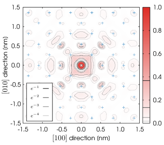
We have calculated the wavefunction, , of the donor electron’s ground state for each of the supercells listed in Table 1. A two dimensional slice of the probability density, , for the largest supercell studied in this work is plotted in Fig. 1. This slice is computed by evaluating the wavefunction in the silicon (001) plane that contains the phosphorus donor. The maximum of the probability density in this slice has been normalized to one. In the (001) plane the majority of the probability density can be seen to be within nm of the donor site, which is located at the origin in Fig. 1. The wavefunction of the donor electron has a form that is similar to an atomic orbital. The corresponding probability density can be seen to decay to approximately 2% of its maximum value at a distance of nm from the donor site in the and crystallographic directions.
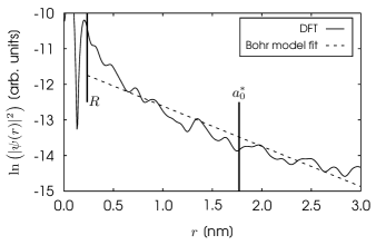
The apparent hydrogenic character of the donor electron’s wavefunction is compatible with an effective Bohr model of the electron. Phosphorus is a shallow defect in silicon so it is reasonable to treat the wavefunction of the Kohn-Sham eigenvalue, calculated within DFT, as an independent single particle state that can be modelled by a simple exponential function. The wavefunction of the donor electron can therefore be described by the envelope function where is a normalisation constant and is an effective Bohr radius. It is then possible to calculate the effective Bohr radius of the donor electron by fitting its wavefunction with this envelope function. However, it is first necessary to spherically average the wavefunction of the donor electron because is radially symmetric and is not.
Figure 2 shows the natural logarithm of the spherically averaged probability density for the phosphorus donor electron, , plotted against radial distance from the donor site, . The domain in this figure includes the core region of the phosphorus atom, which in our model is described by a Troullier-Martins pseudopotential Troullier and Martins (1991). A pseudopotential will deviate from a Coulombic potential in the core region. The envelope function is not applicable within the core region because a hydrogenic wavefunction is not a valid solution here. We have therefore fitted the wavefunction of the donor electron on the domain nm, where is termed the model radius. The model radius must be chosen such that the effects of the core region on the wavefunction do not influence the accuracy of the exponential fit. Nor can the model radius be so large that the whole of the wavefunction’s exponential decay is not captured by the fit. We have set the model radius equal to the atomic nearest neighbour distance, which has a value of 0.235 nm in siliconKittel and Mitchell (1954). As can be seen from Fig. 2, this value for the model radius satisfies our two requirements.
In EMT, it is possible to derive two Bohr radii for the donor electron: one corresponds to the longitudinal effective mass, , of bulk silicon and the other to the transverse mass, . The geometric average of these two radii is given by . By fitting to , we find the effective Bohr radius to be 1.8 nm. This value is in good agreement with 2.087 nm, which is the geometric average of the two effective Bohr radii reported in Ref. Koiller et al., 2001. By reconsidering Fig. 1, we can see that the effective Bohr radius can be thought of as the radial distance within which the vast majority of the probability density corresponding to the donor electron is contained.
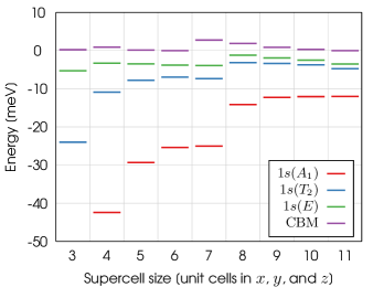
The manifold energy levels for the phosphorus donor electron are shown in Fig. 3. These energies are plotted relative to the conduction band minimum of bulk silicon, calculated using a supercell of 10,648 atoms, which is set to energy zero in the figure. Figure 3 illustrates how the energies of the , , and states increase as the size of the supercell is increased. We suggest the energy levels for the smaller supercells are artifically lowered due to the electron’s interaction with its periodic images, which increases the confinement of the donor electron as the size of the supercell is decreased. The energy levels are converged to within 1 meV for a supercell of 10,648 atoms. These results justify the use of such a large supercell for the calculation of these energies.
The binding energies of the , , and states can be calculated for each supercell by taking the difference between the energy levels and the conduction band minimum of bulk silicon. In Fig. 3 the larger supercells significantly underestimate these energies. This discrepancy is due to the fact the Kohn-Sham eigenvalues are single particle energies and do not correspond exactly to true excitations of the system. This statement applies to energy levels that are unoccupied, as DFT is a ground state theory. We therefore need another way to calculate the binding energies of the manifold energy levels. This is provided by the method described in Ref. Yamamoto et al., 2009, where the binding energy of each state is calculated directly from its wavefunction.
The method of Ref. Yamamoto et al., 2009 allows us to calculate the binding energies of the , , and states directly from their wavefunctions and the impurity potential of the phosphorus donor. We begin by writing down the screened impurity potential of the phosphorus donor; Yamamoto et al. (2009)
| (1) |
where is the Fourier transform of the unscreened impurity potential. The dielectric screening is described by a nonlinear function Nara and Morita (1966); Pantelides and Sah (1974); Wellard and Hollenberg (2005);
| (2) |
with , , , , and the relative permittivity of silicon . The constants , , , and were found by fitting the above function to the dependent dielectric screening in silicon, which was calculated from the random phase approximation Pantelides and Sah (1974). The kinetic and potential energies of the donor electron can then be computed;
| (3) |
and
| (4) |
where is the wavefunction calculated from DFT. Finally, we can calculate the binding energy of the donor electron:
| (5) |
For more information on this derivation, see the supplemental material.
| Exp. & EMT | 45.59 Jagannath et al. (1981) | 33.88 Mayur et al. (1993) | 32.54 Mayur et al. (1993) |
|---|---|---|---|
| EMTKlymenko et al. (2015) | 45.40 | 33.86 | 32.08 |
| BMBWellard and Hollenberg (2005) | 45.5 | 29.1 | 27.1 |
| DFT (this work) | 41 | 32 | 31 |
Table 2 presents the binding energies of the manifold states calculated using experiment, EMT, and DFT. The binding energy of the state calculated using DFT (this work) is equal to 41 meV. This energy is in good agreement with the accepted value of 45.59 meV, which has been calculated from the combination of an experimental measurement Jagannath et al. (1981) and a theoretical correction Faulkner (1969). In addition, we find the binding energies of the excited and states to be 32 meV and 31 meV, respectively. These values are in excellent agreement with the other values listed in Table 2, agreeing to within 2 meV. The binding energies of the two excited states appear to be in better agreement with the accepted values for these energies than the energy of the donor electron’s ground state.
In summary, we have calculated the wavefunction of a phosphorus donor electron in silicon with DFT. This wavefunction is then used to compute the effective Bohr radius of the donor electron. We employ a hydrogenic model of this electron and thereby find its Bohr radius to be 1.8 nm. In addition, we compute the binding energy of the donor electron’s ground state, which is found to be in good agreement with the currently accepted value. The energies of the excited and states are found to be in excellent agreement with the accepted values. These results constitute the first ab initio calculation of the manifold energy levels for a single phosphorus donor in silicon.
This work was supported by computational resources provided by the Australian Government through the National Computational Infrastructure under the National Computational Merit Allocation Scheme. D.W.D. acknowledges the support of the ARC Centre of Excellence for Nanoscale BioPhotonics (CE140100003).
Appendix A Supplemental information
A.1 Density functional theory
The electronic structure calculations were performed with density functional theory (DFT) using the siestapackage Soler et al. (2002); Artacho et al. (2008). We have employed the Perdew-Burke-Ernzerhof (PBE) exchange correlation (XC) functional in the generalised gradient approximation (GGA) Perdew et al. (1996). Application of the GGA to phosphorus-doped silicon systems in the past has produced results that are in good agreement with experiment Liu et al. (2003). The total energies of each of the supercells were converged to within 0.1 meV using a planewave energy cutoff of 300 Ry and a Fermi-Dirac occupation function at a temperature of 0 K. Atomic potentials were described by norm-conserving Troullier-Martins pseudopotentials Troullier and Martins (1991).
We have variationally solved the Kohn-Sham equations using a basis set of localised atomic orbitals that was optimised for phosphorus-doped silicon using the simplex method Budi et al. (2012). The basis set was double- polarised and was comprised of 13 radial functions. In Ref. Drumm et al., 2013a, localised single- and double- polarised bases, and a delocalised planewave basis were used to calculate the valley splitting for a phosphorus doped monolayer in silicon. Despite the higher precision of the planewave basis, the double- polarised basis was shown to “[retain] the physics of the planewave description” Drumm et al. (2013a).
We relaxed the crystallographic structure of bulk silicon using this basis set and found the lattice constant to be 5.4575 Å. This value is in good agreement with the experimental value of 5.431 Å Becker et al. (1982). The overestimation of the lattice constant by approximately 0.5% is lower than the usual systematic deviation of the lattice constant that is expected from the PBE XC functional, which is a 1% deviation.
A.2 Benchmarking of density functional theory
To reduce the computational expense of performing these electronic structure calculations, we have used a point grid that contains only a single point: the point, i.e. . For the supercell of 10,648 atoms, an increase in the size of the point grid would result in these calculations being computationally impractical. When the number of points is increased up to for the supercell of 512 atoms, we find the eigenvalue of the state at the point converges to a value that is approximately 5 meV greater than that of the point calculation. The eigenvalues of the and states converge to values that are approximately 1 meV greater than the result of their respective point calculations. We expect these changes in the eigenvalues of the system to decrease as the size of the supercell is increased because the size of the corresponding Brillouin zone will decrease. Previous calculations of an arsenic donor in silicon with DFT have also been restricted to the point Yamamoto et al. (2009).
We geometrically optimised the ionic positions of supercells that ranged in size from 64 to 4096 atoms. We found the maximum displacement of a silicon atom was largest for the supercell of 64 atoms. When the size of the supercells is increased up to 4096 atoms the maximum displacement decreased to less than 0.02 Å. This displacement is equivalent to less than 0.5% of the lattice constant of bulk silicon. We therefore conclude it is unnecessary to relax the ionic positions of silicon atoms beyond their bulk values for supercells larger than 4096 atoms.
The conduction band minimum (CBM) of silicon is located at , along each of the cardinal axes of reciprocal space, inside the face centred cubic Brillouin zone. Because silicon is an indirect bandgap semiconductor, the energy of the lowest conduction valley at the point is not equal to the energy of the CBM. This is a result of the dispersion of the energy bands. We calculate the eigenvalues of the phosphorus donor electron at , not , and therefore it is necessary to offset the computed energies of the , , and states to find their value at .
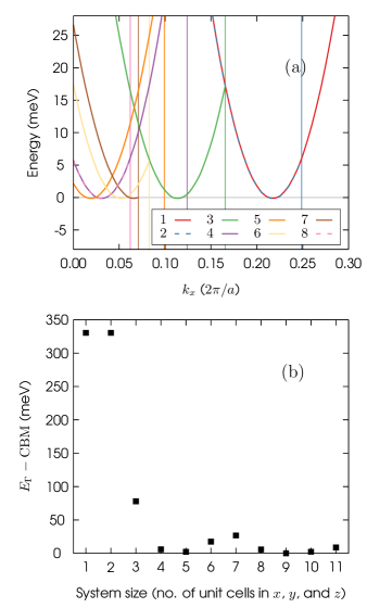
The size of the Brillouin zone is decreased when the size of the supercell is increased. Decreasing the size of the Brillouin zone causes the bands, and therefore CBM, to be folded towards the centre of the zone, i.e. the point, in a process known as band folding Drumm et al. (2013a). Consequently, the amount by which the energies of the , , and states must be offset, to account for the parabolic dispersion of the band, is different for each supercell. The folding of the lowest conduction valley is plotted in Fig. 4a for supercells that range in size from 8 to 4096 atoms. The value of the offset for each supercell can be computed by taking the difference between the energy of the valley at the point () and the conduction-band minimum (CBM). These energies have been plotted for all supercells in Fig. 4b.
The value of decreases as the size of the supercell is increased. As shown in Fig. 4b, this relationship is not monotonic: the CBM is not always folded closer to the point as the size of the Brillouin zone is decreased. Figure 4a shows the lowest conduction valley for bulk silicon only. If the dispersion of this band does not change significantly upon doping with phosphorus, then the difference can be used to correct the computed energies of the , , and states. The positions of the conduction valleys on the axis, in Fig. 4, have been computed by folding the band structure of bulk silicon. The unfolded band structure was calculated using an eight atom simple cubic unit cell and a point grid of . For the sake of clarity, we do not show the part of the bands that are reflected back into the Brillouin zone at the zone boundary. Neither do we show the conduction valleys of supercells with more than 4096 atoms in Fig. 4. The reflection of the bands at the zone boundary is a consequence of the fact that a solution in one Brillouin zone must be a solution in all Brillouin zones Drumm et al. (2013a).
The energy of the lowest conduction valley of bulk silicon at the point () is shown in Fig. 5 for every supercell studied in this work. As expected, the value of is different for each supercell. The conduction band minima plotted in Fig. 5 are for bulk silicon and have been calculated by substracting from , i.e. . The CBM for bulk silicon is not expected to change as the size of the supercell is increased. We therefore use the CBM of the supercell containing 10,648 atoms as a point of reference by setting it to energy zero in the figure.
We find the CBM for each of the supercells do not agree when the energies are corrected for band folding only. We also need to account for the differences in the valence band maximum (VBM) of each supercell. The conduction band minima are shifted by the difference between the VBM of each supercell and the VBM of the supercell containing 10,648 atoms. Once this is done, the CBM in Fig. 5 agree to within 4 meV. The remaining discrepancies in the conduction band minima could be caused by the differing point grids that were used to calculate the quantity and the conduction band minima plotted in Fig. 5, or similar errors in the VBM itself. The VBM is not affected by band folding because it appears at the point in the Brillouin zone.
A.3 Calculation of binding energies
In this section, we give the mathematical details of the calculation of the binding energy for the donor electron in full. This method was first proposed in Ref. Yamamoto et al., 2009 for an arsenic donor in silicon.
The binding energy of the donor electron is given by
| (6) |
where is the kinetic energy and is the potential energy of the donor electron. In (6) the potential energy is defined as
| (7) |
where is the wavefunction of the donor electron and is the impurity potential for the phosphorus donor. The impurity potential can be written as
| (8) |
where is the electric potential for a phosphorus-doped silicon system and is the electric potential for an electron-doped silicon system. By an electron-doped silicon system, we mean a bulk silicon system with one electron added. In contrast, for the phosphorus-doped system, one electron is added to the system by substituting a silicon atom with a phosphorus atom. These two electric potentials can be defined as
| (9) |
and
| (10) |
where is the electron-electron contribution to the electric potential, is the exchange-correlation contribution to the electric potential, and is the electron-nuclear contribution to the electric potential. Substituting (9) and (10) into (8) and rearranging we have
| (11) |
In the equations above, the impurity potential is screened by the electron-electron and exchange-correlation terms. Next, we set and to zero and thereby introduce a new quantity, the unscreened impurity potential . The unscreened impurity potential is given by the last term in (11):
| (12) |
In our calculations, the electron-nuclear interaction is described by Troullier-Martins pseudopotentials and we can write
| (13) |
and
| (14) |
where is the ionic position of the phosphorus donor atom, is the ionic position of silicon atom , and and are the pseudopotentials of phosphorus and silicon, respectively. Substituting (13) and (14) into (12), we obtain
which, because we have not relaxed the ionic positions of the silicon atoms after phosphorus substitution, simplifies to
where is approximate because the norm-consering Troullier-Martins pseudopotentials are nonlocal. Let , then
| (15) |
That is, the unscreened impurity potential is given by the difference in the pseudopotentials for phosphorus and silicon. We have used only the component of the norm-conserving pseudopotentials for phosphorus and silicon when evaluating Eq. 15. This approximation is justified given the structure of the eigenfunction for the state (cf. Fig. 1 in the main text). Electron screening can now be reintroduced using the following description. We rewrite the screened impurity potential as Yamamoto et al. (2009)
| (16) |
where is the Fourier transform of the unscreened impurity potential. The dielectric screening is described by a nonlinear function Pantelides and Sah (1974); Nara and Morita (1966)
| (17) |
with , , , , and . The constants , , , and were found by fitting the above function to the dependent dielectric screening in silicon, which was calculated from the random phase approximation Pantelides and Sah (1974). We can then use (16) to calculate the potential energy of the donor electron using (7). Finally, to calculate the kinetic energy of the donor electron, we use the virial theorem:
| (18) |
The binding energy of the donor electron can then be calculated from the kinetic and potential energies using (6).
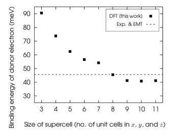
The binding energies of the donor electron’s ground state, calculated using supercells of 216 to 10,648 atoms, are shown in Fig. 6. For the supercell of 10,648 atoms, the value of the binding energy is converged to within 1 meV. The accepted value for the binding energy of the donor electron’s ground state, which is equal to 45.59 meV, is shown as a dashed line in Fig. 6. The supercell of 216 atoms overestimates the binding energy of the state in the figure but the binding energy decreases as the size of the supercell is increased. This energy is within 5 meV of the accepted value for a supercell of 10,648 atoms. Unfortunately there is no systematic way of calculating the uncertainty in this energy, but it is unlikely that the uncertainty is less than 5 meV.
References
- Kane (1998) B. E. Kane, Nature 393, 133 (1998).
- Morello et al. (2010) A. Morello, J. J. Pla, F. A. Zwanenburg, K. W. Chan, K. Y. Tan, H. Huebl, M. Möttönen, C. D. Nugroho, C. Yang, J. A. van Donkelaar, A. D. C. Alves, D. N. Jamieson, C. C. Escott, L. C. L. Hollenberg, R. G. Clark, and A. S. Dzurak, Nature 467, 687 (2010).
- Füchsle et al. (2012) M. Füchsle, J. A. Miwa, S. Mahapatra, H. Ryu, S. Lee, O. Warschkow, L. C. L. Hollenberg, G. Klimeck, and M. Y. Simmons, Nature Nanotechnology 7, 242 (2012).
- Pla et al. (2012) J. J. Pla, K. Y. Tan, J. P. Dehollain, W. H. Lim, J. J. L. Morton, D. N. Jamieson, A. S. Dzurak, and A. Morello, Nature 489, 541 (2012).
- Hill et al. (2015) C. D. Hill, E. Peretz, S. J. Hile, M. G. House, M. Fuechsle, S. Rogge, M. Y. Simmons, and L. C. L. Hollenberg, Science Advances 1, e1500707 (2015).
- Zwanenburg et al. (2013) F. A. Zwanenburg, A. S. Dzurak, A. Morello, M. Y. Simmons, L. C. L. Hollenberg, G. Klimeck, S. Rogge, S. N. Coppersmith, and M. A. Eriksson, Reviews of Modern Physics 85, 961 (2013).
- Füchsle et al. (2010) M. Füchsle, S. Mahapatra, F. A. Zwanenburg, M. Friesen, M. A. Eriksson, and M. Y. Simmons, Nature Nanotechnology 5, 502 (2010).
- Tettamanzi et al. (2014) G. C. Tettamanzi, R. Wacquez, and S. Rogge, New Journal of Physics 16, 063036 (2014).
- Salfi et al. (2014) J. Salfi, J. A. Mol, R. Rahman, G. Klimeck, M. Y. Simmons, L. C. L. Hollenberg, and S. Rogge, Nature materials 13, 605 (2014).
- Usman et al. (2016) M. Usman, J. Bocquel, J. Salfi, B. Voisin, A. Tankasala, R. Rahman, M. Y. Simmons, S. Rogge, and L. C. L. Hollenberg, Nature Nanotechnology , 1 (2016).
- Saraiva et al. (2016) A. L. Saraiva, J. Salfi, J. Bocquel, B. Voisin, S. Rogge, R. B. Capaz, M. J. Calderón, and B. Koiller, Physical Review B 93, 045303 (2016).
- Kohn and Luttinger (1955) W. Kohn and J. M. Luttinger, Physical Review 98, 915 (1955).
- Mayur et al. (1993) A. J. Mayur, M. D. Sciacca, A. K. Ramdas, and S. Rodriguez, Physical Review B 48, 10893 (1993).
- Aggarwal and Ramdas (1965a) R. L. Aggarwal and A. K. Ramdas, Physical Review 137, A602 (1965a).
- Aggarwal (1964) R. L. Aggarwal, Solid State Communications 2, 163 (1964).
- Overhof and Gerstmann (2004) H. Overhof and U. Gerstmann, Physical Review Letters 92, 087602 (2004).
- Yamamoto et al. (2009) T. Yamamoto, T. Uda, T. Yamasaki, and T. Ohno, Physics Letters A 373, 3989 (2009).
- Aggarwal and Ramdas (1965b) R. L. Aggarwal and A. K. Ramdas, Physical Review 140, A1246 (1965b).
- Jagannath et al. (1981) C. Jagannath, Z. W. Grabowski, and A. K. Ramdas, Physical Review B 23, 2082 (1981).
- Faulkner (1969) R. A. Faulkner, Physical Review 184, 713 (1969).
- Klymenko et al. (2015) M. V. Klymenko, S. Rogge, and F. Remacle, Physical Review B 92, 195302 (2015).
- Wellard and Hollenberg (2005) C. J. Wellard and L. C. L. Hollenberg, Physical Review B 72, 085202 (2005).
- Rahman et al. (2007) R. Rahman, C. J. Wellard, F. R. Bradbury, M. Prada, J. H. Cole, G. Klimeck, and L. C. L. Hollenberg, Physical Review Letters 99, 036403 (2007).
- Pica et al. (2014) G. Pica, G. Wolfowicz, M. Urdampilleta, M. L. W. Thewalt, H. Riemann, N. V. Abrosimov, P. Becker, H.-J. Pohl, J. J. L. Morton, R. N. Bhatt, S. a. Lyon, and B. W. Lovett, Physical Review B 90, 195204 (2014).
- Gamble et al. (2015) J. K. Gamble, N. T. Jacobson, E. Nielsen, A. D. Baczewski, J. E. Moussa, I. Montaño, and R. P. Muller, Physical Review B 91, 235318 (2015).
- Greenman et al. (2013) L. Greenman, H. D. Whitley, and K. B. Whaley, Physical Review B 88, 165102 (2013).
- Carter et al. (2011) D. J. Carter, N. A. Marks, O. Warschkow, and D. R. McKenzie, Nanotechnology 22, 065701 (2011).
- Budi et al. (2012) A. Budi, D. W. Drumm, M. C. Per, A. Tregonning, S. P. Russo, and L. C. L. Hollenberg, Physical Review B 86, 165123 (2012).
- Carter et al. (2013) D. J. Carter, O. Warschkow, N. A. Marks, and D. R. McKenzie, Physical Review B 87, 045204 (2013).
- Drumm et al. (2013a) D. W. Drumm, A. Budi, M. C. Per, S. P. Russo, and L. C. L Hollenberg, Nanoscale Research Letters 8, 111 (2013a).
- Drumm et al. (2014) D. W. Drumm, M. C. Per, A. Budi, L. C. L. Hollenberg, and S. P. Russo, Nanoscale Research Letters 9, 443 (2014).
- Drumm et al. (2013b) D. W. Drumm, J. S. Smith, M. C. Per, A. Budi, L. C. L. Hollenberg, and S. P. Russo, Physical Review Letters 110, 126802 (2013b).
- Smith et al. (2015) J. S. Smith, D. W. Drumm, A. Budi, J. A. Vaitkus, J. H. Cole, and S. P. Russo, Physical Review B 92, 235420 (2015).
- Soler et al. (2002) J. M. Soler, E. Artacho, J. D. Gale, A. García, J. Junquera, P. Ordejón, and D. Sánchez-Portal, Journal of Physics: Condensed Matter 14, 2745 (2002).
- Artacho et al. (2008) E. Artacho, E. Anglada, O. Diéguez, J. D. Gale, A. García, J. Junquera, R. M. Martin, P. Ordejón, J. M. Pruneda, D. Sánchez-Portal, and J. M. Soler, Journal of Physics: Condensed Matter 20, 064208 (2008).
- Troullier and Martins (1991) N. Troullier and J. L. Martins, Physical Review B 43, 8861 (1991).
- Kittel and Mitchell (1954) C. Kittel and A. H. Mitchell, Physical Review 96, 1488 (1954).
- Koiller et al. (2001) B. Koiller, X. Hu, and S. Das Sarma, Physical Review Letters 88, 027903 (2001).
- Nara and Morita (1966) H. Nara and A. Morita, Journal of the Physical Society of Japan 21, 1852 (1966).
- Pantelides and Sah (1974) S. Pantelides and C. Sah, Physical Review B 10, 621 (1974).
- Perdew et al. (1996) J. P. Perdew, K. Burke, and M. Ernzerhof, Physical Review Letters 77, 3865 (1996).
- Liu et al. (2003) X.-Y. Liu, W. Windl, K. M. Beardmore, and M. P. Masquelier, Applied Physics Letters 82, 1839 (2003).
- Becker et al. (1982) P. Becker, P. Scyfried, and H. Siegert, Zeitschrift für Physik B Condensed Matter 48, 17 (1982).