CoMET: Composite–Input Magnetoelectric–based Logic Technology
Abstract
This work proposes CoMET, a fast and energy-efficient spintronics device for logic applications. An input voltage is applied to a ferroelectric (FE) material, in contact with a composite structure – a ferromagnet (FM) with in-plane magnetic anisotropy (IMA) placed on top of an intra-gate FM interconnect with perpendicular magnetic anisotropy (PMA). Through the magnetoelectric (ME) effect, the input voltage nucleates a domain wall (DW) at the input end of the PMA-FM interconnect. An applied current then rapidly propagates the DW towards the output FE structure, where the inverse-ME effect generates an output voltage. This voltage is propagated to the input of the next CoMET device using a novel circuit structure that enables efficient device cascading. The material parameters for CoMET are optimized by systematically exploring the impact of parameter choices on device performance. Simulations on a 7nm CoMET device show fast, low-energy operation, with a delay/energy of 99ps/68aJ for INV and 135ps/85aJ for MAJ3.
Index Terms:
Design space exploration, magnetoelecric logic, spintronics.I Introduction
Several spin-based devices have been proposed as alternatives to CMOS [9, 11], leveraging spin-transfer torque (STT) [4, 8, 14, 13], switching a ferromagnet (FM) by transferring electron angular momentum to the magnetic moment; spin-Hall effect (SHE), generating spin current from a charge current through a high resistivity material [27]; magnetoelectric (ME) effect [20], using an electric field to change FM magnetization [26, 31]; domain wall (DW) motion through an FM using automotion [26, 12], an external field [7] or current [36, 21, 14]; dipole coupling between the magnets [25]; and propagating spin wave through an FM [2]. In order for the spin-based processor to be running at a CMOS–competitive clock speed of 1GHz, we need the device delay to be around . Theoretically, some of the proposed devices can achieve this target delay [11] at the cost of additional energy. However, in order to be competitive with CMOS, spin–based device not only has to be fast, but also energy efficient, i.e., its energy dissipation should be in the range of a few hundred aJ.
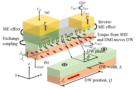
We propose CoMET, a novel device that nucleates a DW in an FM channel with perpendicular magnetic anisotropy (PMA), and uses current-driven DW motion to propagate the signal to the output. A voltage applied on an input ferroelectric (FE) capacitor nucleates the DW through the ME effect. For fast, energy-efficient nucleation, we use a composite structure with an IMA–FM layer above the PMA–FM channel. The DW is propagated to the output end of the PMA channel using a charge current applied to a layer of high resistivity material placed under the PMA channel. The inverse–ME (IME) effect induces a voltage at the output end, and we use a novel circuit structure to transmit the signal to the next stage of logic.
The contributions of our work are as follows:
-
•
The composite structure of IMA–FM/PMA–FM allows DW nucleation under a low applied voltage of . Before the application of a voltage, the magnetization in the PMA–FM is moved away from its easy axis by the strong exchange coupling between IMA–FM/PMA–FM, thus enabling a fast low-power DW nucleation.
-
•
We use charge current to realize fast DW propagation through the PMA–FM interconnect. The current-driven DW motion scheme has been experimentally shown to be fast [28, 30], with demonstrated velocities up to . We choose a PMA channel for DW motion, as against one with in-plane magnetic anisotropy (IMA), since it is more robust to DW pinning and surface roughness effects [33, 29].
-
•
A novel circuit structure comprising a dual–rail inverter allows efficient cascading of devices. This scheme improves upon a previous scheme [26] of 6:1 device ratioing and the need for repeated amplifications.
-
•
We explore the design space of the possible PMA–FM material parameters to optimize the performance of the device. Through this systematic design space exploration, we show that it is possible to achieve inverter delay/energy of /.
The rest of this paper is organized as follows: In Section II, we explain the operation of CoMET. We present the mathematical models and the simulation framework used in this work in Section III. Next, we show the performance of the device as a function of the material parameters in Section IV. Section V concludes the paper.
II CoMET: Device Concept and Operation
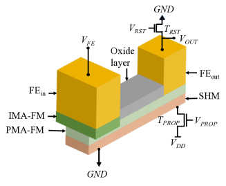
The structure of the proposed device is shown in Fig. 1. At the input, a FE capacitor, , is placed atop an IMA–FM. The IMA–FM is exchange–coupled with the input end of a longer PMA–FM interconnect. At its output end, a second FE capacitor, , is placed on top of the PMA–FM interconnect. A layer of high-resistivity spin-Hall material (SHM), which is conducive to strong spin-orbit interaction, is placed beneath the PMA–FM. An oxide layer is present on top of PMA–FM between and .
II-A CoMET–based inverter
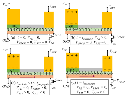
Stage 1 – DW nucleation: At time , an applied voltage, , charges . The resulting electric field across , , may be positive or negative, depending on the sign of , and generates an effective magnetic field, , through the ME effect that couples the electric polarization in FE with the magnetization in the IMA–FM. This magnetic field acts on the composite structure. For , this nucleates a DW in the PMA–FM as seen from Fig. 3(b), with a down–up configuration if the initial magnetization is along the axis. For the opposite case, an up–down configuration is nucleated.
If the initial orientation of the PMA–FM is at an angle to the z-axis, a smaller field can nucleate the DW. The composite structure creates this angle due to strong exchange coupling between the IMA–FM and the PMA–FM as can be seen from the magnetization of PMA–FM in Fig. 3(a), thus allowing nucleation under a low magnitude of . In the absence of IMA–FM, voltages up to are necessary to nucleate a DW whereas we show that with the presence of IMA–FM, voltages as low as would suffice.
Stage 2 – DW propagation Once the DW is nucleated in PMA–FM, transistor is turned on using the signal to send a charge current () through the SHM. Due to SHE, electrons with opposite spin accumulate in the direction transverse to the charge current as shown in Fig. 2. As a result, a spin current () is generated in a direction normal to the plane of SHM. The resultant torque from the combination of SHE and Dzyaloshinskii–Moriya interaction (DMI) [28] at the interface of PMA–FM and the SHM propagates the DW to the output end.
Before the DW reaches the output, turns on transistor to connect to GND as seen from Fig. 3(c). This causes to charge due to the presence of an electric field across it as a result of the IME effect. This step resets the capacitor such that once the DW reaches the output, it can either reverse or maintain the electric polarization of FE, thus reflecting the result of the operation.
Stage 3 – Output FE switching: The DW reaches the output end in time as seen from Fig. 3(d) and switches the magnetization of PMA–FM. The magnetization in PMA–FM couples with the electric polarization of through the IME effect. As a result, a voltage, , is induced at the output node.
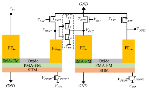
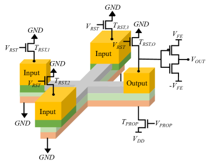
Stage 4 – Cascading multiple logic stages: Successive logic stages of CoMET can be cascaded as shown in Fig. 4(a), through a dual-rail inverter structure comprising transistors and . A timing diagram showing the application of the different input excitations and the output signal are shown in Fig. 4(b). The signal turns on transistors and in the two logic stages to charge the respective FE capacitors. The output voltage induced through the IME effect, , turns on either or , depending on its polarity. These transistors form an inverter and set for the next stage to a polarity opposite that of . The result of the operation is retained in the PMA-FM when the supply voltage is removed. This allows the realization of nonvolatile logic with CoMET. As a result, the inverter can be power-gated after signal transfer, saving leakage. Unlike the charge transfer scheme in [26] with 6:1 ratioing between stages and repeated amplification, our scheme allows all stages to be unit-sized, resulting in area and energy efficiency. This scheme also allows efficient charge-based cascading of logic stages as opposed to spin–based cascading, which require a large number of buffers to overcome the spin losses in the interconnects [15].

II-B CoMET–based Majority gate
The idea of the CoMET inverter can be extended to build a three-input CoMET majority gate (MAJ3), as shown in Fig. 5(a). The input voltage is applied to each input to nucleate a DW in the PMA–FM below each . The DWs from each input is propagated to the output by turning on . The DWs compete in the PMA–FM [8], and the majority prevails to switch using the IME effect. Subsequent gates are cascaded using the dual-rail inverter scheme described above.

III Modeling and simulation framework
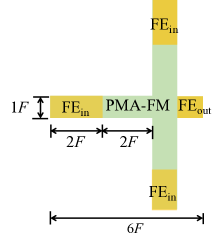
We now show how the performance of a MAJ3 gate can be modeled. The worst–case delay of this gate occurs when one input differs from the others. At feature size, , the DW for each input nucleates in PMA–FM below FE at a distance once is applied. The DW from each input then travels a distance to switch as shown in Fig. 5(b). The dimensions of the simulated structure are shown in Fig. 5(c). The IMA–FM aspect ratio (x:y) is set to 2:1 to align the magnetization of PMA–FM at an angle to the easy axis (due to shape anisotropy). The and thicknesses are set to to avoid leakage through the capacitors. The PMA–FM thickness is set to .
III-A Modeling device operation
We analyze the device operation in each of the four stages as follows:
Stage 1 – DW nucleation: The dynamics of electric polarization, , of due to as a result of the applied voltage across the thickness of the input FE capacitor, are described by the Landau-Khalatnikov (LKh) equation [23]:
| (1) |
where is the total free energy of the input structure as a function of , is the viscosity coefficient, is the component of in the direction, and is the volume of the input FE capacitor. The resultant generates an effective magnetic field from ME, given by,
| (2) |
Here, is the ME interface thickness, denotes the thickness of FE, and refers to the ME coefficient. The magnetic field, is then applied as a Zeeman field to the composite structure in the micromagnetics simulator, OOMMF [22], which solves the Landau-Lifshitz-Gilbert (LLG) equation [16, 34] as shown below, to obtain :
| (3) |
Here refers to the damping constant and denotes the magnetization in PMA–FM. The effective magnetic field, is given by:
| (4) |
where , , and refer to the contributions to from magnetic anisotropy, the demagnetization field, and the exchange field in PMA–FM, respectively.
Stage 2 – DW propagation: The 1D equations that model DW motion describe its instantaneous velocity, and phase [28, 3] (defined in Fig. 2) through a pair of coupled differential equations:
| (5) | ||||
The DW width, [19] is given by,
| (6) |
whereas the effective field from anisotropy (), SHE (), DMI (), and field-like term from STT () is given by,
| (7) | ||||
The contribution of to the motion of the DW in PMA–FM is negligible compared to those from SHE and DMI [28]. Here, , , , , , , , and refer to the exchange constant, PMA–FM saturation magnetization, PMA–FM polarization ratio, PMA–FM thickness, PMA–FM uniaxial anisotropy, adiabatic STT parameter, spin-Hall angle, and DMI constant, respectively. The average DW velocity is used to calculate .
| Parameter | Value |
|---|---|
| Viscosity coefficient, [Vms/K] [26] | 5.4710-5 |
| Vacuum permittivity, [F/m] | 8.8510-12 |
| Vacuum permeability, [Tm/A] | 1.2510-6 |
| Charge of the electron, [C] | 1.6010-19 |
| Gyromagnetic ratio, [rad/sT] | 1.761011 |
| Speed of light, c [m/s] | 3108 |
| ME coefficient for FE, [s/m] [10] | (0.2/c) |
| ME coefficient for FE, [s/m] [10] | (1.4/c) |
| Resistivity of SHM, [-m] [28] | 1.0610-7 |
| FE permittivity, [26] | 164 |
| Adiabatic STT parameter, [28] | 0.4 |
| DMI constant, [mJ/m2] [28, 3] | 0.8 |
| ME interface thickness, [nm] [26] | 1.5 |
| Transistor threshold voltage, [V] [1] | 0.2 |
| Bohr magneton, [J/T] | 9.27410-24 |
| Transistor on-resistance, [] [1] | 3480 |
| Transistor on-resistance, [] [1] | 4109 |
| Spin Hall angle, | 0.5 |
| Spin polarization, [28] | 0.5 |
| Transistor gate capacitance, [fF] [1] | 0.1 |
Stage 3 – Output FE switching: The electric field developed across from IME effect, , due to the magnetization, in PMA–FM is used to calculate as shown below:
| (8) | ||||
where is the inverse ME coefficient [10], is the interface thickness, and refers to the thickness of the output FE capacitor.
Stage 4 – Cascading logic stages: The time, , required to transfer to the input of the next stage includes the delay of the dual-rail inverter and the RC delay of the wire from the inverter output to of the next stage.
III-B Modeling performance parameters
The delay and energy of a -input CoMET majority gate are:
| (9) | ||||
where , , , and , respectively, refer to the energy for charging the , turning the transistors on, SHM Joule heating, and due to transistor leakage currents. The factor of is due to PMA–FM magnetization initialization of each input to a state that allows DW nucleation [26]. Finally,
Here, , , , and refer to the transistor gate capacitance, capacitance of the input FE capacitor, transistor on–resistance, and resistance of the SHM, respectively. The length, width, and thickness of the SHM, are respectively, given by , , and , each with subscript SHM.
III-C Layout of CoMET–based majority gate
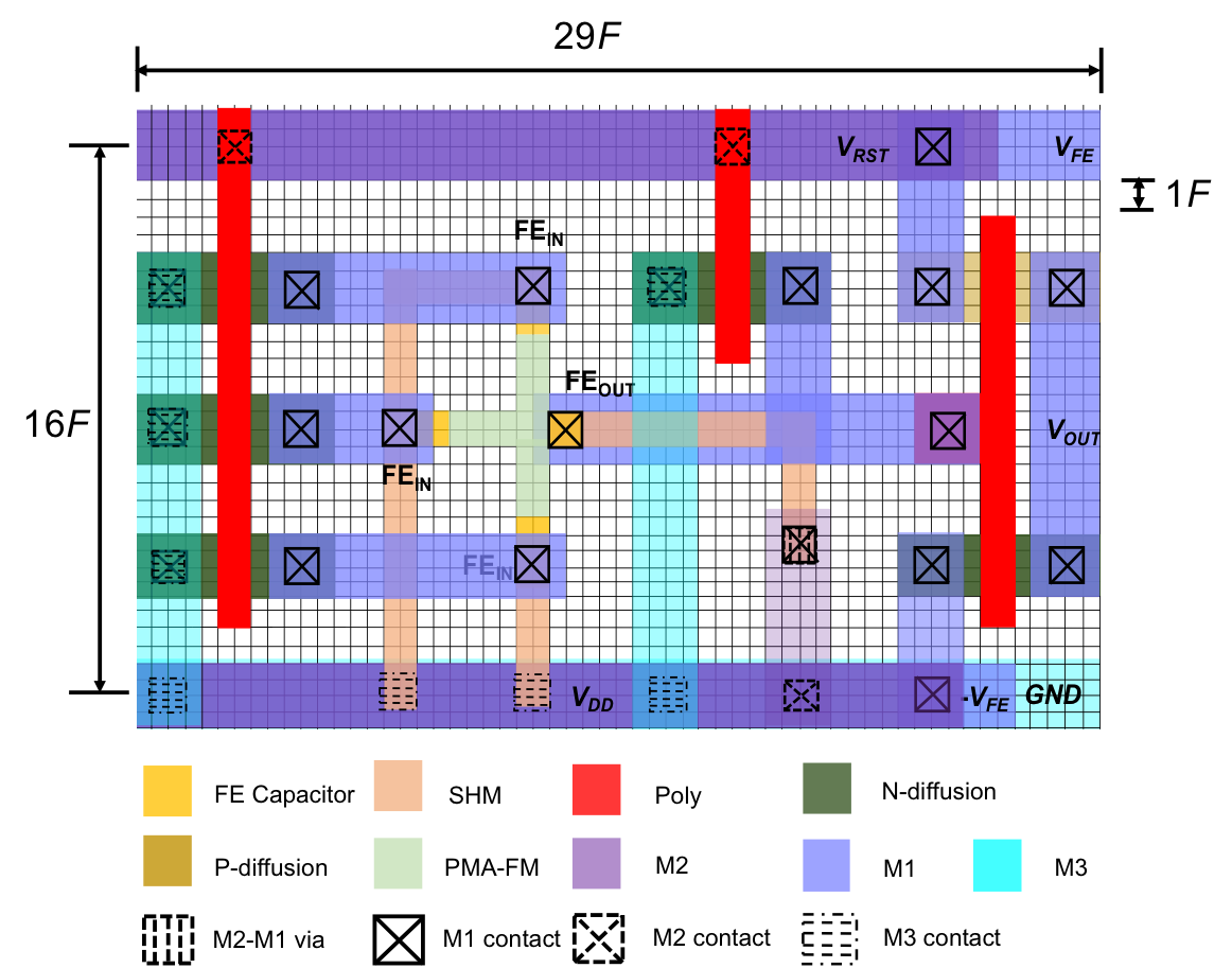
The layout of MAJ3 corresponding to the schematic shown in Fig. 5 for a chosen value of , is shown in Fig. 6. We draw the layout according to the design rules for as described in detail in [9]. The reset transistor for each input FE capacitor , , with , and the reset transistor for the output FE capacitor, , are local to the majority gate as shown in the layout. The transistor required to send a charge current through the SHM, , is shared globally by multiple gates. The dual-rail inverter is local to the majority gate and transfers the information to the next stage. The area of the MAJ3 gate is nm2.
IV Results and Discussion
The delay of the device is a function of the dimensions of IMA–FM and PMA–FM material parameters, specifically , , , and . We explore the design space consisting of the combination of these parameters and analyze their impact on device performance. We demonstrate the results of the design space exploration for and show two sample design points for set to and .
IV-A Choice of material parameters
The simulation parameters and their values used in this work are listed in Table I. The parameter space is chosen to reflect realistic values: the choice of is chosen to reflect the typical exchange constant of existing and exploratory ferromagnetic materials. Lowering further would make the Curie temperature too low [24]. The choice of and allow the mapping of PMA–FM materials to existing materials. The choice of is free of any constraint to material mapping as it can be modified by adequately doping the PMA–FM [35, 32]. The saturation magnetization of the IMA–FM, is set to . The value of and for the IMA–FM is set to the same value as that of PMA–FM.
IV-B DW nucleation
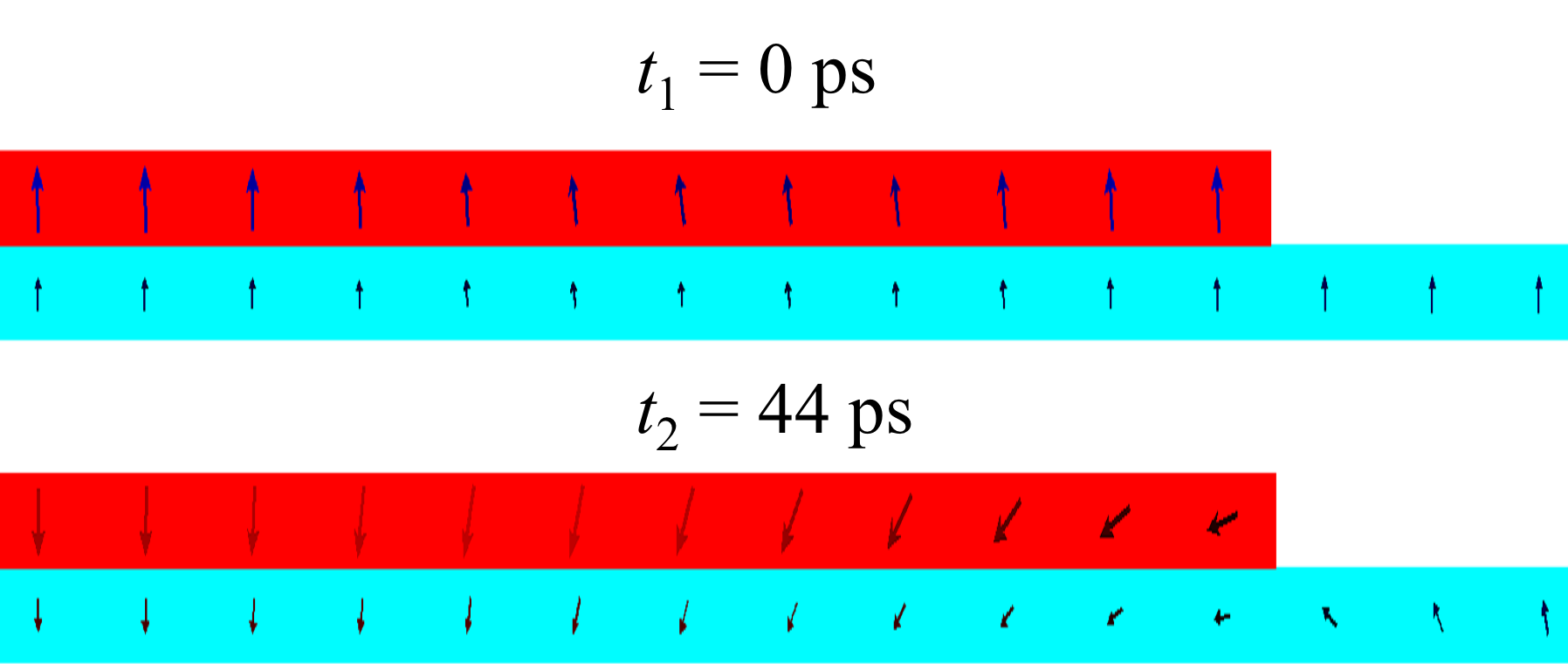
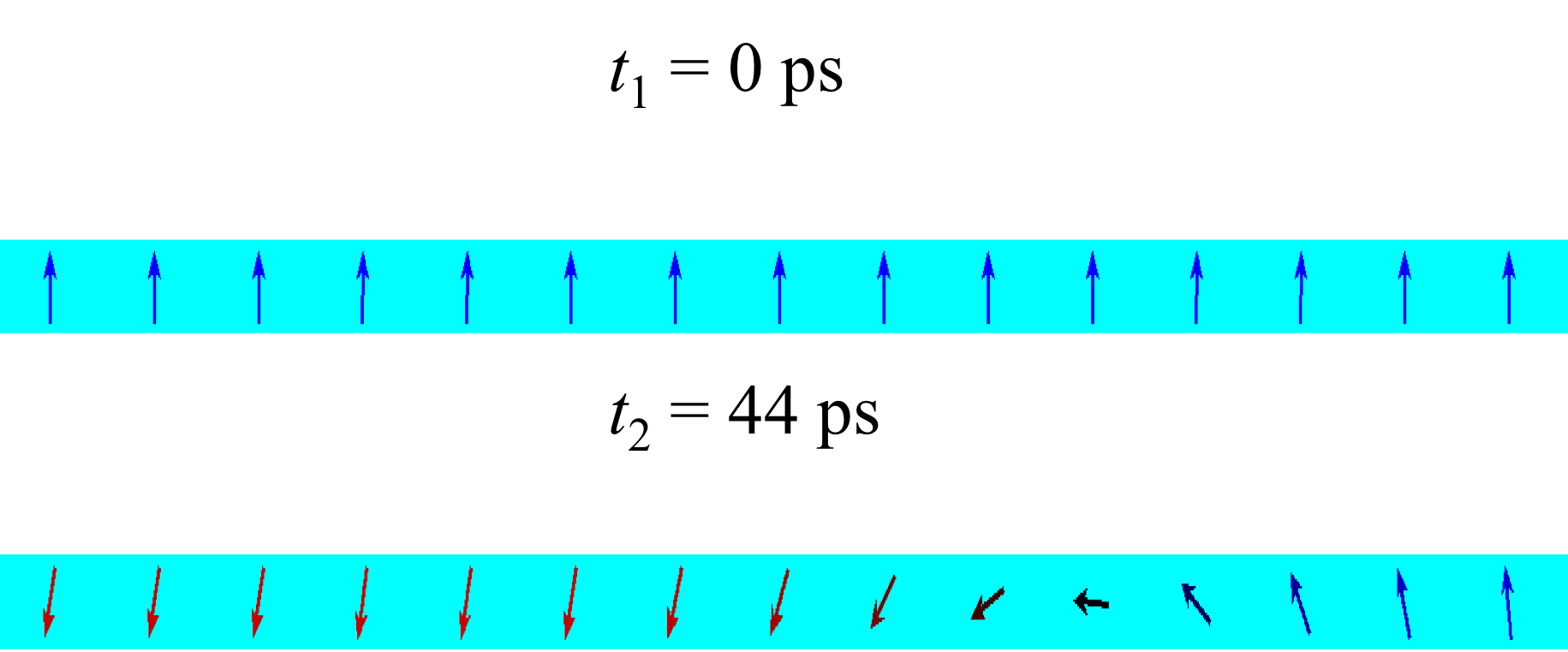
We estimate in OOMMF when the DW nucleates beneath the IMA–FM as shown in the snapshots in Fig. 7(a). We first relax the composite structure in OOMMF for before applying the effective ME field as a Zeeman field. This time period allows the PMA–FM to reach an equilibrium state before the DW is nucleated. In a typical circuit, this state could be achieved by the PMA–FM in the time interval between successive switching activity. At the end of , denoted in the figure as , the magnetization of the PMA–FM rests at an angle to the easy axis owing to the strong exchange coupling with the IMA–FM. After applying a Zeeman field, the DW nucleates in PMA–FM at after a delay of .
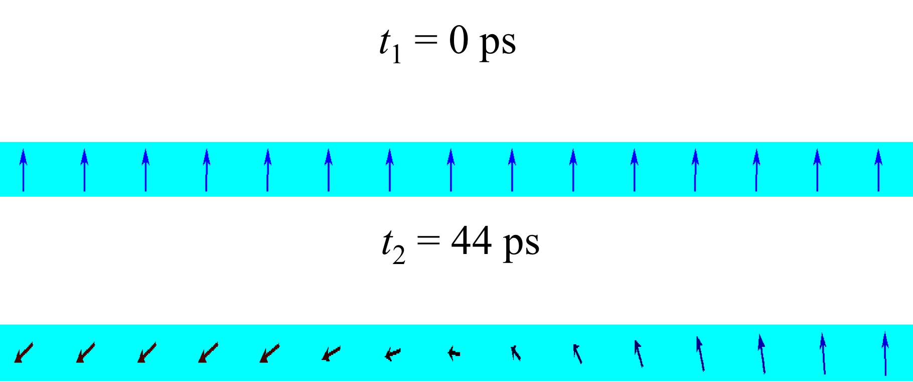
We compare the voltages required to nucleate the DW in the PMA–FM at approximately the same , in the absence of the IMA–FM on top of the PMA–FM to provide the initial angle. The procedure to calculate is identical to the experiment in Fig. 7(a). We perform this analysis for two cases: (i) when the applied Zeeman field acts on a region nm corresponding to the scenario shown in Fig. 7(b). The DW nucleates at at . However, required to generate the DW is now . After relaxing the magnetization for , an absence of IMA–FM translates to a very low initial angle at which necessitates a stronger effective ME field, , and therefore a higher to nucleate the DW for a given . (ii) The absence of IMA–FM allows us to further compact the CoMET device such that the FE capacitor dimensions are the minimum possible at a chosen value of . This corresponds to the dimensions, nm (as opposed to those shown in Fig. 5(c)), the region from the left end of PMA–FM on which acts. We find that the voltage required to nucleate the DW at , as shown in Fig. 7(c), is close to . From these two experiments, we conclude that the composite structure facilitates a fast and energy-efficient DW nucleation.
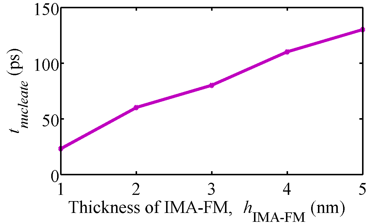
The nucleation of DW in the PMA–FM is not only a function of PMA–FM material parameters, but also depends on the material dimensions of the IMA–FM. As stated in Section III, the aspect ratio of the IMA–FM is set to 2:1 to obtain the shape anisotropy necessary for the coupling with PMA–FM. We then explore the dependence of on the thickness of IMA–FM, and plot the results in Fig. 8. As increases, it becomes harder to switch the PMA–FM due to strong exchange coupling between IMA–FM and PMA–FM, increasing . We therefore select .
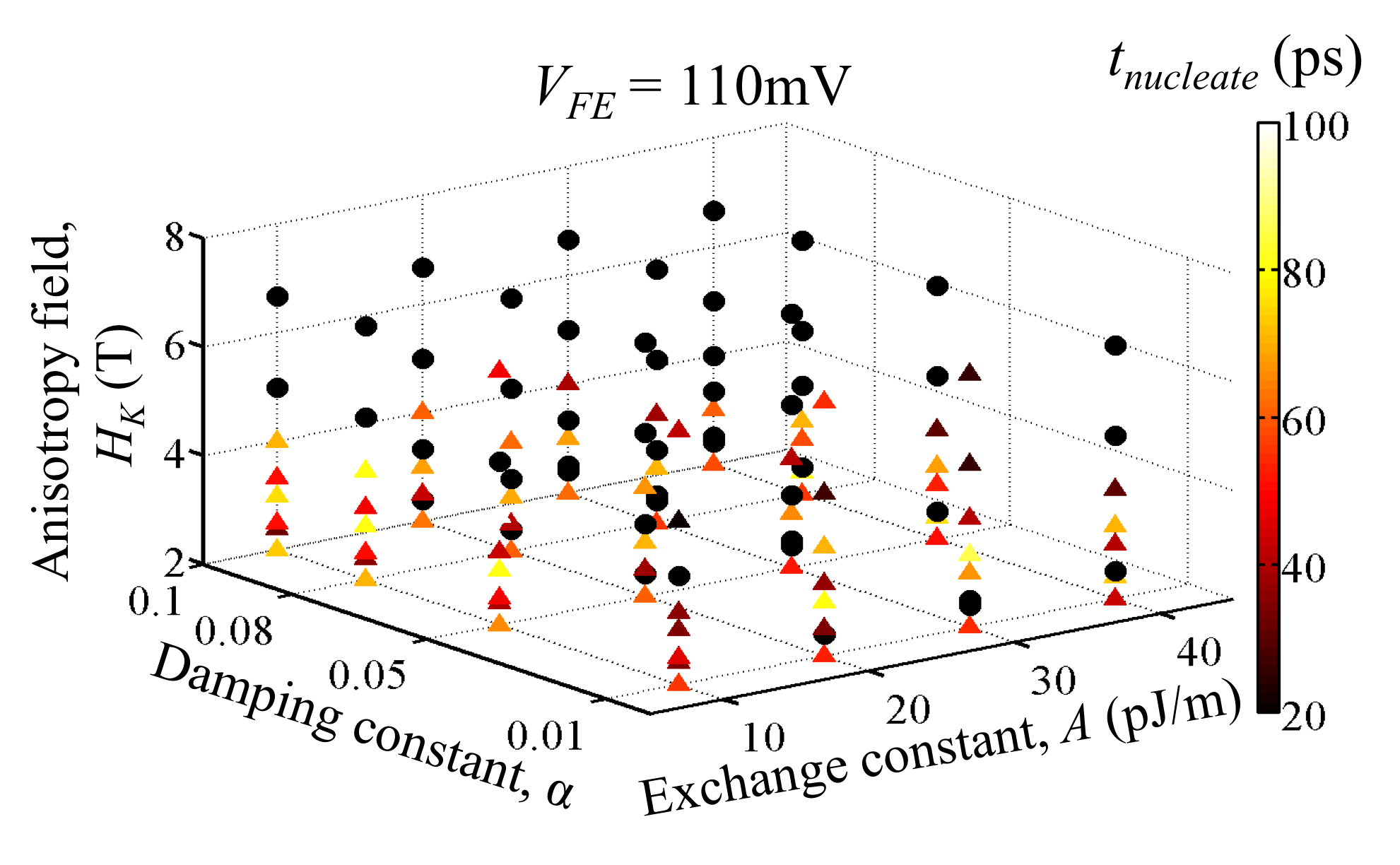
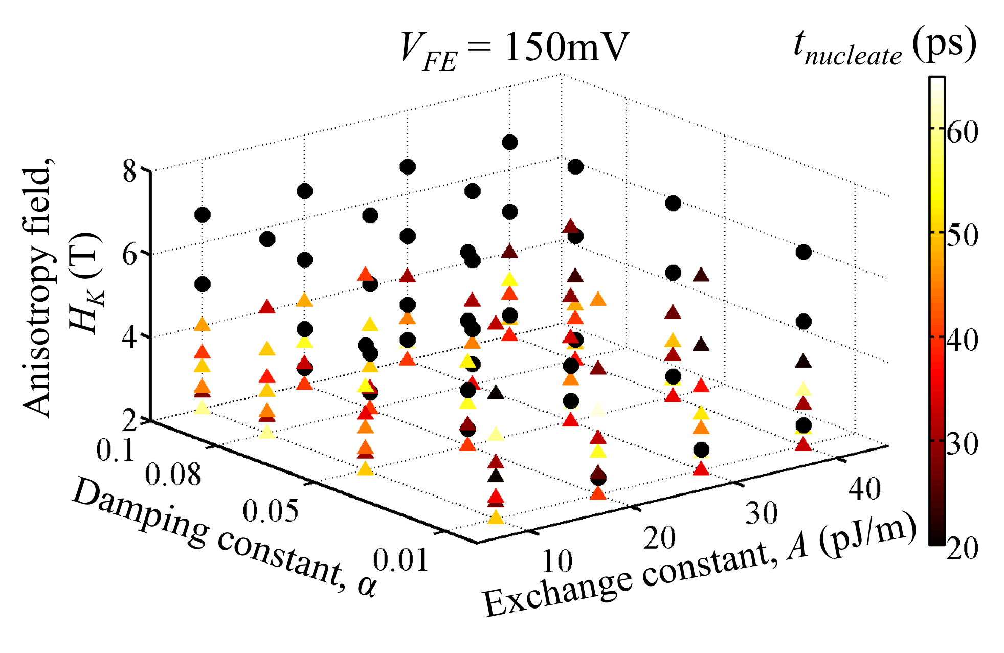
The impact of material parameters of PMA–FM on is shown in Fig. 9(a) and Fig. 9(b) for and , respectively. It is seen that (a) a larger reduces , and this can be shown to be consistent with the DW nucleation Equations (1–3). A larger corresponds to a larger across FE, which in turn creates a larger to nucleate the DW faster. (b) Lower values of are more conducive to nucleation; a lower anisotropy field makes it easier for to switch the magnetization between the two easy axes and (c) low values of reduce owing to the weaker exchange coupling with the neighboring magnetic domains of the PMA–FM. We note that for , the number of design points at which the nucleation does not occur increases. Therefore we pick the lowest value of . This choice does not restrict the design search space for DW propagation as is primarily dictated by the choice of .
IV-C DW propagation
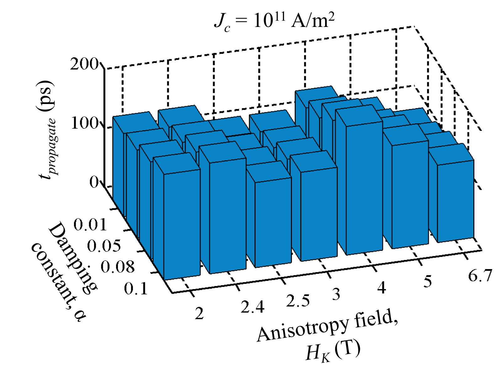
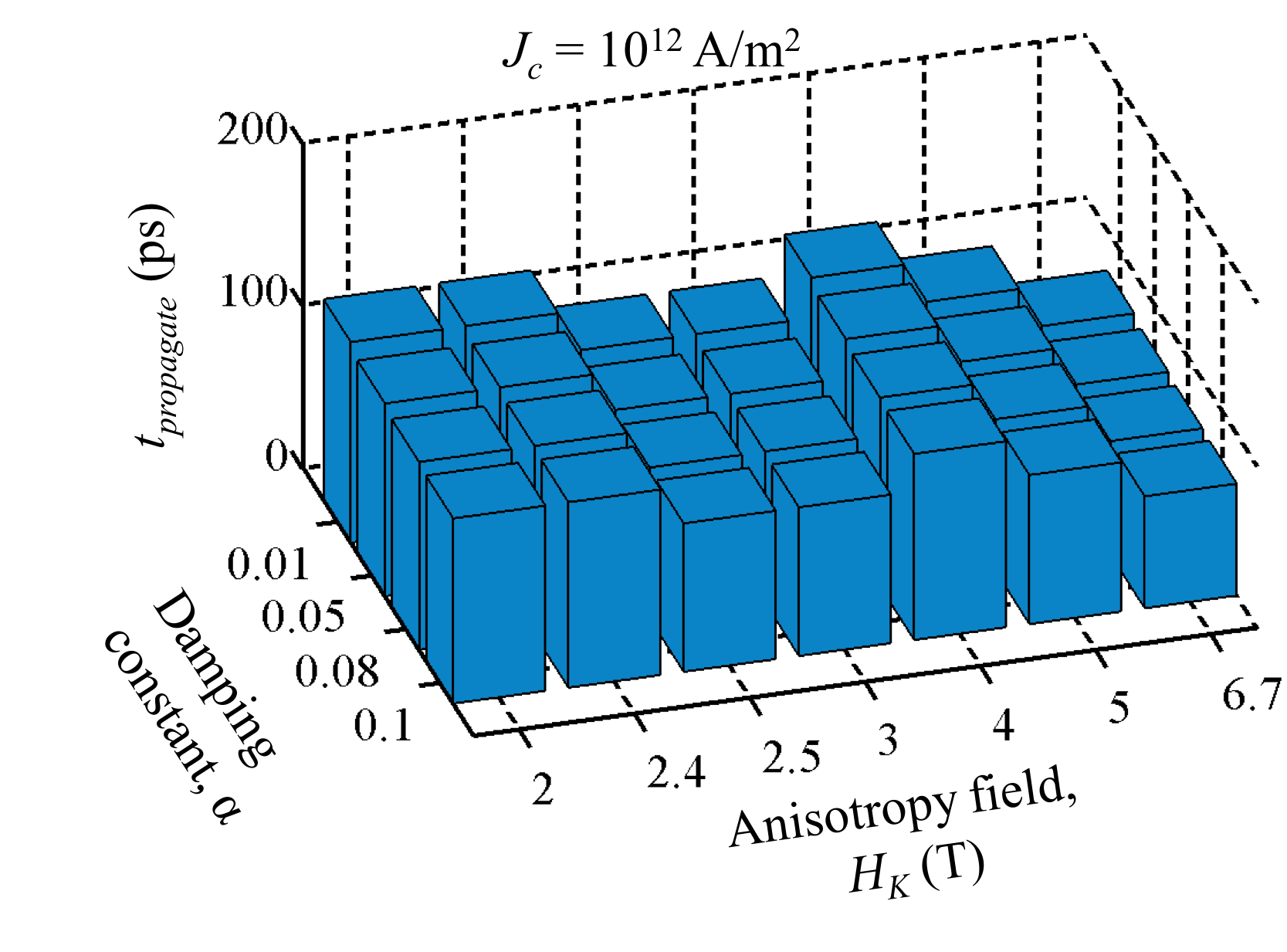
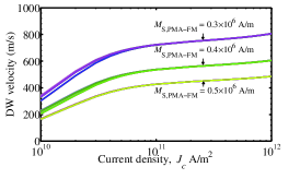
With this choice, we show for A/m2 and A/m2 in Figs. 10(a) and (b), respectively. Increasing increases the torque from SHE as seen from the expressions for in Equation 7. This can be seen from Fig. 10(c) where increasing increases the DW velocity, thereby reducing . These curves lie in three clusters, and show the dominance of over other parameters.
This can also be seen from Figs. 10(a) and (b) where the lowest bars () correspond to . This is consistent with the Equation 7: a lower implies higher and , and therefore higher DW velocity.
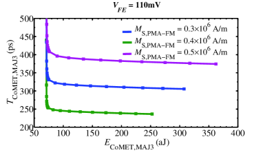
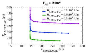
IV-D Performance evaluation
For the three corresponding to each of the three clusters in Fig. 10(c), we plot vs. for MAJ3 in Fig. 11 for the two values of . The dual–rail inverter delay, , is calculated using the PTM technology models [1]. For a chosen and , the energy-delay data points are obtained by increasing from to in discrete steps. The main observations from Fig. 11 are as follows:
-
•
Increasing is seen to reduce by reducing , at the expense of a larger .
-
•
A higher corresponds to lower , but is only marginally higher since it is primarily dominated by the transistor energy.
-
•
Initially when increases, reduces at the same rate as , thus keeping the energy approximately constant. After a certain point, increasing only gives marginal improvements in delay. This result is consistent with Fig. 10(c); as increases from A/m2 to A/m2, DW velocity increases sharply initially but only increases gradually later.
-
•
A robust design point can be chosen such that is less variable with material parameters. This corresponds to the right portion of each curve where the delay only improves marginally with increase in .
| (mV) | (ps) | (ps) | (ps) | (ps) |
|---|---|---|---|---|
| 110 | 35/35 | 77.4/38.7 | 8.8/8.8 | 242.4/165.5 |
| 150 | 30/30 | 77.4/38.7 | 8.2/8.2 | 231.2/153.8 |
| (mV) | (aJ) | (aJ) | (aJ) | (aJ) | (aJ) |
|---|---|---|---|---|---|
| 110 | 2.4/0.8 | 40.8/24.2 | 19.8/1.6 | 16.3/16.3 | 158.6/85.8 |
| 150 | 4.4/1.5 | 42.0/30.6 | 25.5/1.5 | 22.8/22.8 | 189.4/112.8 |
(A)
| (mV) | (ps) | (ps) | (ps) | (ps) |
|---|---|---|---|---|
| 110 | 30/30 | 36.2/18.1 | 7.9/7.9 | 148.2/112.0 |
| 150 | 25/25 | 36.2/18.1 | 6.2/6.2 | 134.8/98.6 |
| (mV) | (aJ) | (aJ) | (aJ) | (aJ) | (aJ) |
|---|---|---|---|---|---|
| 110 | 0.5/0.1 | 16.8/12.0 | 1.8/0.1 | 13.7/13.7 | 65.6/51.8 |
| 150 | 0.9/0.3 | 21.4/15.3 | 1.8/0.1 | 18.5/18.5 | 85.2/68.4 |
(B)
The best (, ) for each for MAJ3/INV for and are shown in Table II(A) and (B), respectively. It can be seen that dominates while is dominated by energy associated with turning the transistors on and the corresponding leakage. The delay and energy obtained using the CMOS technology given respectively by (, ) for an inverter is () at and () at . For CMOS-based MAJ3 gate, the performance numbers are (14.8ps, 704.2aJ) at and () at . The CMOS performance numbers were obtained using the PTM technology models [1] at nominal supply voltages of for and for . Thus we see that a MAJ3 gate can be implemented more energy-efficiently with CoMET than with CMOS.
At these design points, , , and can be mapped to MnGa–based Heusler alloy [6, 20]. The damping constant, can be engineered by choosing a new composition of PMA–FM. For the FE layer, BiFeO3 (BFO) can be used [26], while the SHM could be -W, Pt, -Ta [17, 18, 5] or some new materials under investigation.
V Conclusion
A novel spintronic logic device based on magnetoelectric effect and fast current–driven domain wall propagation has been proposed. We have shown that the composite input structure of a FM with IMA placed in contact with a PMA–FM allows circuit operation at low voltages of and V. A novel circuit structure comprising a dual–rail inverter structure for efficient logic cascading has also been introduced. The impact of the different material parameters on the performance of the device is then systematically explored. An optimized INV has a delay of with energy dissipation of at 7nm, while a MAJ3 gate runs at and .
Acknowledgment
This work was supported in part by C-SPIN, one of the six SRC STARnet Centers, sponsored by MARCO and DARPA. The authors thank Dr. Angeline Klemm Smith and Dr. Chenyun Pan for their inputs.
References
- [1] “Predictive Technology Model,” http://ptm.asu.edu, accessed: 2016-08-09.
- [2] A. Khitun and K. L. Wang, “Nano scale computational architectures with spin wave bus,” Superlattices and Microstructures, vol. 38, no. 3, pp. 184–200, 2005.
- [3] A. Thiaville, S. Rohart, E. Jué, V. Cros, and A. Fert, “Dynamics of Dzyaloshinskii domain walls in ultrathin magnetic films,” Europhysics Letters, vol. 100, no. 5, pp. 57 002–1–57 002–6, Dec 2012.
- [4] B. Behin-Aein, D. Datta, S. Salahuddin, and S. Datta, “Proposal for an all–spin logic device with built–in memory,” Nature Nanotechnology, vol. 5, no. 4, pp. 266–270, Feb 2010.
- [5] C. F. Pai, L. Liu, Y. Li, H. W. Tseng, D. C. Ralph, and R. A. Buhrman, “Spin transfer torque devices utilizing the giant spin Hall effect of Tungsten,” Applied Physics Letters, vol. 101, no. 12, pp. 122 404–1–122 404–4, Sep 2012.
- [6] C. L. Zha, R. K. Dumas, J. W. Lau, S. M. Mohseni, S. R. Sani, I. V. Golosovsky, Å. F. Monsen, J. Nogués, and J. Åkerman, “Nanostructured MnGa films on Si/SiO2 with 20.5 kOe room temperature coercivity,” Journal of Applied Physics, vol. 110, no. 9, pp. 093 902–1–093 902–4, Nov 2011.
- [7] D. A. Allwood, G. Xiong, C. C. Faulkner, D. Atkinson, D. Petit, and R. P. Cowburn, “Magnetic domain–wall logic,” Science, vol. 309, no. 5741, pp. 1688–1692, Sep 2005.
- [8] D. E. Nikonov, G. I. Bourianoff, and T. Ghani, “Proposal of a spin torque majority gate logic,” IEEE Electron Device Letters, vol. 32, no. 8, pp. 1128–1130, Aug 2011.
- [9] D. E. Nikonov and I. A. Young, “Overview of beyond–CMOS devices and a uniform methodology for their benchmarking,” Proceedings of the IEEE, vol. 101, no. 12, pp. 2498–2533, Dec 2013.
- [10] D. E. Nikonov and I. A. Young, “Benchmarking spintronic logic devices based on magnetoelectric oxides,” Journal of Materials Research, vol. 29, pp. 2109–2115, Sep 2014.
- [11] D. E. Nikonov and I. A. Young, “Benchmarking of beyond–CMOS exploratory devices for logic integrated circuits,” IEEE Journal on Exploratory Solid–State Computational Devices and Circuits, vol. 1, pp. 3–11, Dec 2015.
- [12] D. E. Nikonov, S. Manipatruni, and I. A. Young, “Automotion of domain walls for spintronic interconnects,” Journal of Applied Physics, vol. 115, no. 21, pp. 213 902–1–213 902–5, 2014.
- [13] D. M. Bromberg, D. H. Morris, L. Pileggi, and J. G. Zhu, “Novel STT–MTJ device enabling all–metallic logic circuits,” IEEE Transactions on Magnetics, vol. 48, no. 11, pp. 3215–3218, Nov 2012.
- [14] J. A. Currivan, Y. Jang, M. D. Mascaro, M. A. Baldo, and C. A. Ross, “Low energy magnetic domain wall logic in short, narrow, ferromagnetic wires,” IEEE Magnetics Letters, vol. 3, pp. 3 000 104–1–3 000 104–4, Apr 2012.
- [15] J. Kim, A. Paul, P. A. Crowell, S. J. Koester, S. S. Sapatnekar, J. P. Wang, and C. H. Kim, “Spin–based computing: Device concepts, current status, and a case study on a high–performance microprocessor,” Proceedings of the IEEE, vol. 103, no. 1, pp. 106–130, Jan 2015.
- [16] L. D. Landau and E. Lifshitz, “On the theory of the dispersion of magnetic permeability in ferromagnetic bodies,” Phys. Z. Sowjetunion, vol. 8, pp. 153–169, 1935.
- [17] L. Liu, C. F. Pai, Y. Li, H. W. Tseng, D. C. Ralph, and R. A. Buhrman, “Spin-torque switching with the giant spin Hall effect of Tantalum,” Science, vol. 336, no. 6081, pp. 555–558, May 2012.
- [18] L. Liu, O. J. Lee, T. J. Gudmundsen, D. C. Ralph, and R. A. Buhrman, “Current-induced switching of perpendicularly magnetized magnetic layers using spin torque from the spin Hall effect,” Physical Review Letters, vol. 109, no. 9, pp. 096 602–1–096 602–5, Aug 2012.
- [19] L. Thomas and S. S. Parkin, “Current induced domain-wall motion in magnetic nanowires,” in Handbook of Magnetism and Advanced Magnetic Materials. Wiley Online Library, 2007.
- [20] M. Fiebig, “Revival of the magnetoelectric effect,” Journal of Physics D: Applied Physics, vol. 38, no. 8, pp. R123–R152, April 2005.
- [21] M. G. Mankalale, Z. Liang, A. K. Smith, D. C. Mahendra, M. Jamali, J. P. Wang, and S. S. Sapatnekar, “A fast magnetoelectric device based on current–driven domain wall propagation,” in Proceedings of the 74th IEEE Device Research Conference, June 2016.
- [22] M. J. Donahue and D. G. Porter, OOMMF User’s Guide. US Department of Commerce, Technology Administration, National Institute of Standards and Technology, 1999.
- [23] P. P. Horley, A. Sukhov, C. Jia, E. Martínez, and J. Berakdar, “Influence of magnetoelectric coupling on electric field induced magnetization reversal in a composite unstrained multiferroic chain,” Physical Review B, vol. 85, pp. 054 401–1–054 401–6, Feb 2012.
- [24] R. C. O’Handley, Modern Magnetic Materials: Principles and Applications. Wiley, 1999.
- [25] R. P. Cowburn and M. E. Welland, “Room temperature magnetic quantum cellular automata,” Science, vol. 287, no. 5457, pp. 1466–1468, Feb 2000.
- [26] S. C. Chang, S. Manipatruni, D. E. Nikonov, and I. A. Young, “Clocked domain wall logic using magnetoelectric effects,” IEEE Journal on Exploratory Solid–State Computational Devices and Circuits, (to appear; early version available on IEEE Xplore).
- [27] S. Datta, S. Salahuddin, and B. Behin-Aein, “Non–volatile spin switch for Boolean and non–Boolean logic,” Applied Physics Letters, vol. 101, no. 25, pp. 252 411–1–252 411–5, Dec 2012.
- [28] S. Emori, U. Bauer, S. M. Ahn, E. Martinez, and G. S. D. Beach, “Current–driven dynamics of chiral ferromagnetic domain walls,” Nature Materials, vol. 12, no. 7, pp. 611–616, June 2013.
- [29] S. Fukami, T. Suzuki, N. Ohshima, K. Nagahara, and N. Ishiwata, “Micromagnetic analysis of current driven domain wall motion in nanostrips with perpendicular magnetic anisotropy,” Journal of Applied Physics, vol. 103, no. 7, pp. 07E718–1–07E718–4, Jan 2008.
- [30] S. H. Yang, K. S. Ryu, and S. S. Parkin, “Domain–wall velocities of up to 750 ms-1 driven by exchange–coupling torque in synthetic antiferromagnets,” Nature Nanotechnology, vol. 10, no. 3, pp. 221–226, Feb 2015.
- [31] S. Manipatruni, D. E. Nikonov, and I. A. Young, “Spin-orbit logic with magnetoelectric nodes: A scalable charge mediated nonvolatile spintronic logic,” 2015, available at https://arxiv.org/abs/1512.05428.
- [32] S. Mizukami, T. Kubota, X. Zhang, H. Naganuma, M. Oogane, Y. Ando, and T. Miyazaki, “Influence of Pt doping on Gilbert damping in permalloy films and comparison with the perpendicularly magnetized alloy films,” Japanese Journal of Applied Physics, vol. 50, no. 10R, pp. 103 003–1–103 003–5, Oct 2011.
- [33] T. A. Moore, I. M. Miron, G. Gaudin, G. Serret, S. Auffret, B. Rodmacq, A. Schuhl, S. Pizzini, J. Vogel, and M. Bonfim, “High domain wall velocities induced by current in ultrathin Pt/Co/AlOx wires with perpendicular magnetic anisotropy,” Applied Physics Letters, vol. 93, no. 26, pp. 262 504–1–262 504–4, Dec 2008.
- [34] T. L. Gilbert, “A phenomenological theory of damping in ferromagnetic materials,” IEEE Transactions on Magnetics, vol. 40, no. 6, pp. 3443–3449, Nov 2004.
- [35] W. Bailey, P. Kabos, F. Mancoff, and S. Russek, “Control of magnetization dynamics in Ni81Fe19 thin films through the use of rare-earth dopants,” IEEE Transactions on Magnetics, vol. 37, no. 4, pp. 1749–1754, July 2001.
- [36] X. Yao, J. Harms, A. Lyle, F. Ebrahimi, Y. Zhang, and J. P. Wang, “Magnetic tunnel junction–based spintronic logic units operated by spin transfer torque,” IEEE Transactions on Nanotechnology, vol. 11, no. 1, pp. 120–126, Jan 2012.