Coupled Mode Theory for Semiconductor Nanowires
Abstract
We present a model to describe the spatiotemporal evolution of guided modes in semiconductor nanowires based on a coupled mode formalism. Light-matter interaction is modelled based on semiconductor Bloch equations, including many-particle effects in the screened Hartree-Fock approximation. Appropriate boundary conditions are used to incorporate reflections at waveguide endfacets, thus allowing for the simulation of nanowire lasing. We compute the emission characteristics and temporal dynamics of and nanowire lasers and compare our results both to Finite-Difference Time-Domain simulations and to experimental data. Finally, we explore the dependence of the lasing emission on the nanowire cavity and on the materials relaxation time.
I Introduction
An increasing demand for fast communication technologies and the limitations inherent to electronic integrated circuits has stimulated the research on nanophotonic components. In particular semiconductor nanowires have gathered widespread interest due to their simple fabrication and their remarkable photonic properties, which allow them to act as efficient waveguides and as resonators either for photonic and plasmonic lasing or for harnessing polaritonic effects.Duan et al. (2003); Oulton et al. (2009); Sidiropoulos et al. (2014); Saxena et al. (2013); Röder et al. (2013)
Semiconductor nanowires are complex photonic systems supporting multiple longitudinal as well as transverse modes interacting through the nonlinear response of the medium. The optical properties of the medium are influenced by many-body effects of the excited carriers, which give rise to excitonic absorption peaks and the appearance of polaritons in the weakly excited regime. In the strongly excited regime, effects like phase-space filling, screening and excitation-induced dephasing dominate the optical response,ElSayed et al. (1994); Manzke and Henneberger (2002); Chow and Koch (1999); Haug and Koch (2004) giving rise to a broad gain profile. In order to make correct predictions across the different regimes of excitation conditions, theoretical models of light-matter interaction in semiconductor nanowires need to incorporate all these effects.
Recently, we proposed a coupled Finite-Difference Time-Domain (FDTD)Yee (1966); Taflove and Hagness (2005) and semiconductor Bloch equations (SBEs)Haug and Koch (2004); Chow and Koch (1999) approach to the modelling of light-matter interaction in arbitrary semiconductor geometriesBuschlinger et al. (2015). A similiar approach has also been applied to the description of semiconductor quantum wells.Guazzotti et al. (2016) While models based on the FDTD method are the most general, the numerical complexity can be decreased considerably if assumptions are made concerning the simulated geometry.
In the present case we deal with nanowires, where the propagating fields can be decomposed into waveguide eigenmodes. A considerable simplification of the numerical treatment is achieved by describing the evolution of the eigenmode amplitudes in the framework of coupled mode theory (CMT). In the general case a transverse resolution is needed, but considerably less data points than in the case of a more general approach like FDTD are necessary. The resulting reduction in computational demands makes it possible to increase the simulated time window and the size and complexity of the nanowire geometry or to include even more sophisticated material models capturing additional effects relevant for semiconductor lasers as comprehensively summarized in Böhringer and Hess (2008a, b).
In this paper, we describe our coupled mode theory for semiconductor nanowires including the treatment of reflecting endfacets. We apply the model to the simulation of the temporal dynamics of nanowire-lasers and compare our results to data from an experimental studyWille et al. (2016).
II Theoretical model
II.1 Derivation of propagation equations
In the following, we summarize the derivation of evolution equations for the slowly varying envelopes of waveguide modes under the influence of material nonlinearities and dispersion, which have been used in similiar form by other authors.Crosignani et al. (1981); Snyder and Love (1983) We start with Maxwell’s equations in the frequency domain
| (1) |
| (2) |
The polarization term couples the material model including dispersion, absorption and nonlinearity to the equations for the electromagnetic fields. We consider a waveguide extending in the -direction, which in the unperturbed case () supports modes with the transverse field profiles , and the propagation constants . Neglecting group velocity dispersion, the propagation constant close to the frequency takes the form
| (3) |
with and being the modes inverse group velocity at . Note, that by using this simplification we merely neglegt the group velocity dispersion arising from the frequency-dependent changes of the mode shape. Any dispersion effects caused by the resonant excitation of the semiconductor material remain unaffected.
The fields propagating in the perturbed waveguide () can be decomposed into propagating modes as
| (4) |
| (5) |
We now analyze the vector , which can be interpreted as the contribution of mode to the Poynting vector. Using equations (1) and (2), we find that
| (6) |
Next we integrate equation with respect to the transverse coordinates and . As decays exponentially with and approaching infinity, we obtain
| (7) |
Next, we insert the mode expansion (4),(5) into equation (7). Due to the orthogonality of the modes, we obtain the expression
| (8) |
using the guided power of mode defined as
| (9) |
We insert equation (3) and transform equation (8) back to the time-domain using the inverse Fourier transforms and . We further define slowly varying envelopes for the mode amplitudes
| (10) |
and for the polarization
| (11) |
and arrive at the evolution equation
| (12) |
for the slowly varying envelopes with the driving term
| (13) |
The self-consistent electric field driving the polarization used in equation (13) is given as a superposition of all modes, taking into account the individual mode shapes. For some applications it can be desirable to include a pump field , which mainly propagates in directions perpendicular to the waveguide axis and therefore does not contribute to the guided modes directly. Thus, the self-consistent field is described as
| (14) | |||
II.2 Material Model
| Parameter | Description | Value | Value |
|---|---|---|---|
| Gap energy valence band a | |||
| Gap energy valence band b | |||
| Gap energy valence band c | - | ||
| Effective mass electrons | |||
| Effective mass valence band a | |||
| Effective mass valence band b | |||
| Effective mass valence band c | - | ||
| Background refractive index | |||
| Dipole matrix element | |||
| Polarization dephasing rate | |||
| Carrier recombination rate | |||
| Intraband relaxation rate | |||
| Intraband relaxation rate holes | |||
| Rel. rate valence band b to a | |||
| Rel. rate valence band c to a | - |
To complete the description of the system, the polarization has to be modelled by a separate evolution equation governed by the material system. We use the model published in Ref. Buschlinger et al. (2015), which we shortly summarize here. Our model uses a semiconductor Bloch equationsHaug and Koch (2004); Chow and Koch (1999) approach including many-particle effects in the Screened Hartree-Fock approximation and is adapted to 2-6 semiconductors.Buschlinger et al. (2015) The microscopic polarizations as well as the occupation numbers for conduction-band electrons () and for holes in the different valence bands () are assumed to depend only on the absolute value of the Bloch vector . Then, the complex polarization in a bulk semiconductor takes the form
| (15) |
where is the dipole matrix element attributed to the transition from valence band to the conduction band and coupling to the electric field component pointing in direction . The evolution of the microscopic polarizations is described byHaug and Koch (2004); Chow and Koch (1999)
| (16) |
where are renormalized Rabi-frequencies
| (17) |
The transition energies are given by the sum of the renormalized single-particle energies
| (18) |
of species and the band gap of each transition . In order to correctly describe the highly excited semiconductor, the renormalized Rabi-frequencies and transition-energies are calculated using the screened Coulomb matrix-elements instead of the unscreened matrix elements .Haug and Koch (2004); Buschlinger et al. (2015) Therefore the inclusion of the Coulomb-hole contribution
| (19) |
is neccessary.Chow and Koch (1999) Finally, describes the excitation-density dependent damping of the polarizationBuschlinger et al. (2015); Hügel et al. (2000); Haug (2000) and represents a noise term driving spontaneous emission.Andreasen and Cao (2009, 2010)
The time evolution of the occupation numbers is given by
| (20) |
for electrons and by
| (21) |
for holes in the valence band . The first term describes the carrier excitation by the electromagnetic field. The two terms involving and respectively describe non-radiative recombination and intra-band relaxation of carriers towards Fermi-Dirac distributions with a band dependent fermi level Huang and Ho (2006). To allow for the relaxation between valence bands, an additional contribution is included in the equation of motion for the hole populations, with
| (22) |
Similiar as in the case of the polarization, noise terms and are added to the evolution equations for the electron and hole occupation numbers.
2-6 semiconductors are uniaxial crystals with the optical axis or c-axis pointing along the wire in -direction. Optical transitions occur between a single s-like conduction band (occupation number ) and three valence bands (occupation numbers ).Thomas and Hopfield (1959, 1962) Assuming conservation of electron spin, allowed transitions are characterized by a conservation of angular momenta of photons and electrons. From this, we obtain the transitions , coupling to fields polarized in the -direction perpendicularly to the crystals -axis and the transitions coupling to the fields polarized in -direction pointing along the -axis.Thomas and Hopfield (1959, 1962); Buschlinger et al. (2015)
The model parameters used in this publication are summarized in table 1. For the verification of the model in section III, we compare CMT and FDTD simulations of an optically pumped nanowire laser. In accordance with the FDTD code developed in Buschlinger et al. (2015) we neglect any coupling to valence band , since the excitation is assumed to be close to the fundamental band gap. In contrast, the third valence band is included for the simulations of -nanowire lasers presented in section IV, since the excitation frequency lies above the respective band gap.
II.3 Numerical Considerations
Equation (12) is discretized on an equally spaced grid in both time and propagation length
using central finite differences with temporal and spatial discretization steps correlated as
| (23) |
Only for this choice numerical instabilities can be avoided. We obtain the discretized propagation equations
| (24) |
If a material polarization as described in section II.2 is discretized using central finite differences, the driving terms have to be evaluated on temporally staggered timesteps . As an approximation to the values required for an exact evaluation of equation (24), which are also staggered in space, we use .
The transverse integral over the waveguide cross-section in equation (13) can be evaluated using a spatial discretization scheme appropriate for the waveguide geometry. Usually the transverse resolution can be kept low, using only few data points. For instance we use a resolution of 4 radial steps and 16 azimuthal steps for our simulations of a waveguide with a radius of presented below. In the case of single-mode waveguides there is no interaction between modes with different spatial profiles. Therefore the transverse resolution can in principle be restricted to a single point and the effects of the spatial mode shape can be approximated using effective values for and . In multimode-waveguides a higher transverse resolution has to be used, since both the coupling strength and the phase of the induced polarization have a different spatial dependence for the individual modes. For good quantitative agreement for example with the FDTD method, a transverse resolution has to be used even in the single-mode case. Therefore our model is designed to allow both for effective 1D simulations and for arbitrary transverse resolutions.
Especially for the simulation of lasing nanowires, where the interference between forward and backward propagating waves is strong and intensities vary on the scale of , we have to chose a fine longitudinal discretization for the determination of the material response given by . Due to the stability criterion (23), this resolution requirement also determines the temporal resolution. The material equations however are not subject to this stabilty criterion, since they merely have to resolve the highest frequencies present in the slowly varying envelopes. Since in our case the computational demands are mainly determined by the solution of the material equations, we can further reduce the time needed for computation by restricting the number of timesteps at which the SBEs are evaluated. This can be accomplished by skipping every timesteps in the evaluation of the SBEs and using linear interpolation whenever values from intermediate steps are required. In our lasing example, we can restrict the evaluation of the material equations to every th step. However this number is determined by the detuning between material resonance and envelope center frequency and by the shape of the envelope signals themselves and could be higher or lower depending on the simulated scenario.
The field evolution inside the nanowire laser is heavily influenced by boundary conditions, which we will discuss next. Reflecting boundaries like the endfacets of a nanowire laser cavity can be implemented by inserting the appropriate amplitudes propagating away from the interface. Assuming that equation (14) is evaluated on points with spatial indices , general expressions for the two missing amplitudes at the boundaries are
| (25) | ||||
| (26) |
The reflectivity matrix elementsMaslov and Ning (2003) as well as the mode profiles , and the pump field have to be determined beforehand by analytical estimates or with numerical tools like FDTD using the nondispersive and linear background refractive index of the nanowire material. In the unperturbed propagation equations (), the prescribed reflectivities are the only source of reflection from the endfacets. If the mode amplitudes are coupled to the material equations, there exists an additional contribution to the reflectivity which is caused by the missing material polarization outside the simulation volume. While the prescribed reflectivities describe the reflection at the endfacet of a nanowire with the materials background index , this contribution accounts for the reflectity caused by the electronic part of the refractive index.
III Verification
To verify our method, we compare it to direct simulations of light propagation in semiconductor nanowires using the coupled FDTD and semiconductor Bloch equations approach.Buschlinger et al. (2015)
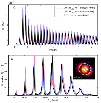
Due to the initial exponential growth in intensity and the strength of nonlinear effects, nanowire lasers constitute an extremely demanding test case for our model. We now consider a highly excited () nanowire laser with length and radius . At a central wavelength of , the wire only supports the two degenerate fundamental modes as shown in the inset of Fig. 1(b)), propagating with group velocity and propagation constant . To create a laser cavity, the wire is terminated by realistic endfacets with an amplitude reflectivity matrix as used in equations (25) and (26)
| (27) |
extracted from a simple linear FDTD simulation of a wire endfacetMaslov and Ning (2003). The occupation probabilities for electrons and holes are initialized with Fermi-distributions at for spatial densities of , . In order to avoid a randomization of the lasing output which would render direct comparisons between the two codes difficult, we switch off spontaneous emission and instead start the laser with a sech-shaped seed pulse with a pulse duration of . The spatial resolution in the FDTD simulation is . In the CMT simulation we use a longitudinal resolution of , while the transverse fields are sampled using a cylindrical coordinate system with radial steps. Due to the high mode confinement, the modal fields have a significant longitudinal contribution, which is not radially symmetric. Therefore, also an azimuthal resolution with steps is neccessary in order to achieve good agreement with FDTD simulations. We use both simulations where the material equations are solved on the same temporal grid as the propagation equations () and on a grid with . In this special case the simulation becomes unstable, if we try to further reduce the temporal resolution of the material equations. However the CMT variety with already is approximately 400 times as fast as the FDTD method.
Fig. 1(a) shows the time-resolved electrical field strength recorded at one endfacet of the nanowire. Since the seed pulse is amplified and reflected inside the cavity, a train of pulses is emitted at the endfacet. We initially observe a fast rise in lasing intensity. After the inversion in the spectral region of the main longitudinal mode has been depleted, the emission switches to other longitudinal modes with lower gain, leading to a slow decay in the lasing intensity similiar to the results in Buschlinger et al. (2015). Despite the dramatically reduced computation time, the CMT results show excellent agreement with the FDTD results concerning the spectral position of the lasing modes(Fig. 1(b)). The temporal dynamics (Fig. 1(a)) also show good qualitative agreement concerning the shape of the emitted pulse train as well as the position of the individual pulses, which is directly linked to the modal dispersion under the influence of the material system. However, the overall intensity of the emitted pulse train is higher in the CMT simulation. Near-perfect agreement can be achieved by tuning of the endfacet reflectivity used by the CMT code. From this we conclude, that the difference in emission intensity is caused by the imperfect modelling of the endfacet reflectivity under the influence of the material system, which is an inherent limitation of Coupled Mode Theory. However, the endfacet reflectivities of real nanowires will always vary due to imperfections in growth and preparation, giving rise to fluctuations of laser performance in experiments. Most importantly, the essential laser dynamics are already captured very well by our model.
IV Temporal dynamics of Nanowire Lasers
Since the increased efficiency of the presented model allows us to simulate the entire excitation and lasing process in a comparatively short time, it is now possible to perform a more comprehensive analysis of the properties of semiconductor nanowire lasers. In our further analysis, we choose wires () due to the wealth of available experimental dataWille et al. (2016); Röder et al. (2015, 2016) for this material system. We specifically model our nanowires after experiments performed by Wille et al. Wille et al. (2016), where time-resolved -PL measurements have been used in order to investigate the temporal dynamics of the lasing emission. An important parameter extracted from the experiment is the emission onset time , which is defined as the time between the maximum of the pump pulse and the buildup of the laser emission to of its maximum. In the lasing regime, the inverse emission onset time is reported to increase nonlinearly with increasing pump power. Additionally, time-resolved spectra have been obtained from the experiment and a spectral red-shift of the lasing modes occuring during emission has been observed. This has been attributed to the depletion of excited carriers due to stimulated emission, which leads to an increase of the refractive index and therefore to a shift in the energies of the wires longitudinal Fabry-Perot modes.
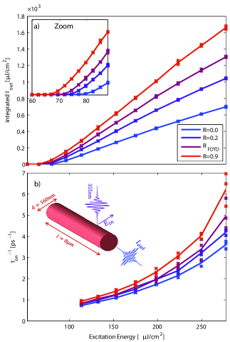
While the main goal of our simulations is the reproduction of the experimental features outlined above, we are additionally going to investigate the dependence of the laser emission on parameters which can vary from sample to sample and are not easily accessible in experiments. We study exemplary nanowires with a length and a diameter of as sketched in the inset of Fig. 2(b). Since the wire diameter is definitely in the single-mode regime, we restrict our simulations to the fundamental mode with a propagation constant and group velocity . The diagonal endfacet reflectivity extracted from FDTD simulations is slightly lower than for the -wire. To decrease simulation time, we restrict the transverse resolution to a single point. This will not exactly reproduce results as they would be obtained by an FDTD-simulation, but allows us to capture the essential physics in the present case of a single-mode wire. The wires are optically pumped from above with sech-shaped pulses with a temporal width of and a central wavelength of , polarized perpendicularly to the wire axis. The exciting field is assumed to be homogeneous along the wire. Since the output can vary from realization to realization due to different random seed values for the spontaneous emission noise in equations (16), (20) and (21), we average over several simulation runs. As the fluctuations are not excessively strong, the averaging procedure is restricted to three runs.
First, we investigate the emission properties of several wires with varying endfacet reflectivity in the range between the extreme values and and including the reflectivity as extracted from FDTD simulations. The endfacet reflectivity of real nanowires can vary strongly between different samples and strongly affects the quality of the optical cavity. Note, that simulations with a nominal endfacet reflectivity of still have a finite reflectivity due to the material boundary effect described in section II.3. The input/output curves resulting from our simulations are given in Fig.2(a) and show the typical lasing behaviour which exhibits a linear increase above a certain threshold intensity of approximately . The laser threshold power lies below the experimental value of , but is of the same order of magnitude. This is to be expected, since we prescribe a homogeneous electric field inside the wire and do not take into account effects like scattering of the exciting waves from the wire or a spatially inhomogeneous excitation. As expected, wires with lower endfacet reflectivities achieve a lower efficiency. Fig.2(b) shows the inverse emission onset time . As reported in the experiment, lasing generally sets in faster with increasing excitation power. We also observe an increase of for higher endfacet reflectivities. Since our model does not include an excitation-dependent carrier relaxation time, this increase can be explained solely by the fact that the laser threshold is reached at an earlier time, if a stronger pump pulse is used. The same effect occurs, if we lower the lasing threshold by increasing the endfacet reflectivity (see inset of Fig. 2(a)). Additionally, roundtrip losses are lowered in this case, allowing for a faster buildup of lasing oscillations.
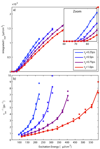
After having investigated the influence of the optical cavity by simulating wires with different endfacet reflectivities, we now consider the influence of the semiconductor relaxation dynamics, which are governed by the intraband relaxation time .
Fig. 3(a) shows simulated input/output curves for different values of . We observe a decreasing lasing efficiency for increasing intraband relaxation times. This is due to the fact, that the lasing process is slowed down for high relaxation times. Thus, a higher number of carriers can recombine by the way of other relaxation processes before being used for spontaneous emission. As expected, the slowed down dynamics also leads to a strong decrease in the inverse emission onset time (3(b)). However, the nonlinear increase of with increasing pump power is retained for all simulated values of .
Finally, we use a windowed Fourier-transform in order to obtain the time-resolved lasing spectrum (Fig. 4(b)) of one of our wire configurations with and , which produces similiar temporal dynamics as measured in the experiment.Wille et al. (2016)
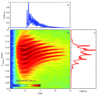
The temporal lasing profile and the time-averaged spectrum are given in (Fig. 4) (a) and (c), respectively. Similiar to the experiment, we observe a pronounced red-shift of the lasing modes during the emission process due to the change in the materials refractive index caused by the depletion of quasi-particles.

Since the most computationally demanding part of our model is the evaluation of the Coulomb terms, it would be desirable to simplify the model in this regard. Therefore we also examine the influence of the Coulomb interaction on the laser performance of our exemplary -nanowire (Fig. 5). Several changes can already be predicted by considering the differences in the linear absorption and gain spectra for the full model (blue lines in Fig. 5(a)) and the free-carrier model (red lines) at low excitation ( , faded lines) and at high excitation (, strong lines). First, the Coulomb interaction leads to a well-known enhancement of the overall optical responseHaug and Koch (2004); Chow and Koch (1999). If the Coulomb interaction is omitted, we expect a decrease in absorption at the pump wavelength, leading to a higher laser threshold and a decreased laser efficiency. Second, the omission of the various Coulomb-related shifts in the quasi-particle energies will lead to a significant blue-shift of the gain region, which now will be positioned almost exclusively at energies above the bandgap. It is possible to artificially correct this by including the Coulomb-hole shift (Eq. (19)) into the free carrier model. Even though this is physically not meaningful in the context of an interaction-free model, the position of the gain region can be partly corrected in this way (violet curves in Fig. 5). The corresponding lasing curves are shown in Fig. 5(b). As it turns out, the decreased density of states and the lack of Coulomb-related energy shifts in the free-carrier model(red curve) completely obstruct optical pumping up to the laser threshold for a pump-wavelength of , since the relevant transitions saturate before the neccessary excitation density is reached. For the artificially corrected model with the Coulomb-hole shift included (violet curve), we observe lasing. However as we would expect, we observe an increased laser threshold and a decreased efficiency as compared to the full model(blue curve). We conclude, that an omission of the Coulomb interaction terms leads to significant differences in the predicted performance and spectral properties of semiconductor lasers. A thus reduced model requires significant tuning of parameters in order to yield meaningful results.
V Conclusion
In conclusion, we have developed a new theoretical model for the simulation of light-matter interaction and lasing in semiconductor nanowire structures based on the framework of coupled mode theory coupled to semiconductor Bloch equations. We have shown that our model can qualitatively and quantitatively reproduce the results achieved by a more general FDTD model, but with a speedup of up to three orders of magnitude depending on the simulated setup and the required accuracy. We have further applied the model to the simulation of the properties and temporal dynamics of -nanowire lasers. We reproduce the red-shift of the lasing modes occuring during the emission process as well as the nonlinear increase of the inverse emission onset time with increasing excitation power, which have been observed in experimentsWille et al. (2016). Further, we have studied the influence of the optical cavity as well as the carrier relaxation time on the laser dynamics. We observe a reduction of the emission onset time both with increasing endfacet reflectivity and with decreasing material relaxation time. In the future, the computational efficiency of our model is going to pave the way for the inclusion of more advanced material models as well as more complicated geometries in full time-domain simulations of semiconductor nanowires.
Acknowledgements.
The authors gratefully acknowledge financial support by Deutsche Forschungsgemeinschaft (Forschergruppe FOR1616, projects P5 and E4). The authors thank Robert Röder and Marcel Wille for helpful discussions.References
- Duan et al. (2003) Xiangfeng Duan, Yu Huang, Ritesh Agarwal, and Charles M. Lieber, “Single-nanowire electrically driven lasers,” Nature 421, 241–245 (2003).
- Oulton et al. (2009) Rupert F. Oulton, Volker J. Sorger, Thomas Zentgraf, Ren-Min Ma, Christopher Gladden, Lun Dai, Guy Bartal, and Xiang Zhang, “Plasmon lasers at deep subwavelength scale,” Nature 461, 629–632 (2009).
- Sidiropoulos et al. (2014) Themistoklis P. H. Sidiropoulos, Robert Röder, Sebastian Geburt, Ortwin Hess, Stefan A. Maier, Carsten Ronning, and Rupert F. Oulton, “Ultrafast plasmonic nanowire lasers near the surface plasmon frequency,” Nature Physics 10, 870–876 (2014).
- Saxena et al. (2013) Dhruv Saxena, Sudha Mokkapati, Patrick Parkinson, Nian Jiang, Qiang Gao, Hark Hoe Tan, and Chennupati Jagadish, “Optically pumped room-temperature gaas nanowire lasers,” Nature Photonics 7, 963–968 (2013).
- Röder et al. (2013) Robert Röder, Marcel Wille, Sebastian Geburt, Jura Rensberg, Mengyao Zhang, Jia Grace Lu, Federico Capasso, Robert Buschlinger, Ulf Peschel, and Carsten Ronning, “Continuous wave nanowire lasing,” Nano Letters 13, 3602–3606 (2013), http://pubs.acs.org/doi/pdf/10.1021/nl401355b .
- ElSayed et al. (1994) K. ElSayed, L. Bányai, and H. Haug, “Coulomb quantum kinetics and optical dephasing on the femtosecond time scale,” Phys. Rev. B 50, 1541 (1994).
- Manzke and Henneberger (2002) G. Manzke and K. Henneberger, “Quantum-kinetic effects in the linear optical response of GaAs quantum wells,” phys. stat. sol. (b) 234, 233 (2002).
- Chow and Koch (1999) W.W. Chow and S.W. Koch, Semiconductor-Laser Fundamentals: Physics of the Gain Materials (Springer, 1999).
- Haug and Koch (2004) H. Haug and S.W. Koch, Quantum Theory of the Optical and Electronic Properties of Semiconductors (4th Edition) (World Scientific, 2004).
- Yee (1966) Kane S. Yee, “Numerical solution of initial boundary value problems involving maxwells equations in isotropic media,” IEEE Trans. Antennas and Propagation , 302–307 (1966).
- Taflove and Hagness (2005) Allen Taflove and Susan C. Hagness, Computational Electrodynamics: The Finite-Difference Time-Domain Method, Third Edition, 3rd ed. (Artech House, 2005).
- Buschlinger et al. (2015) Robert Buschlinger, Michael Lorke, and Ulf Peschel, “Light-matter interaction and lasing in semiconductor nanowires: A combined finite-difference time-domain and semiconductor bloch equation approach,” Phys. Rev. B 91, 045203 (2015).
- Guazzotti et al. (2016) Stefano Guazzotti, Andreas Pusch, Doris E. Reiter, and Ortwin Hess, “Dynamical calculation of third-harmonic generation in a semiconductor quantum well,” Phys. Rev. B 94, 115303 (2016).
- Böhringer and Hess (2008a) Klaus Böhringer and Ortwin Hess, “A full-time-domain approach to spatio-temporal dynamics of semiconductor lasers. i. theoretical formulation,” Progress in Quantum Electronics 32, 159–246 (2008a).
- Böhringer and Hess (2008b) Klaus Böhringer and Ortwin Hess, “A full time-domain approach to spatio-temporal dynamics of semiconductor lasers. ii. spatio-temporal dynamics,” Progress in Quantum Electronics 32, 247–307 (2008b).
- Wille et al. (2016) Marcel Wille, Chris Sturm, Tom Michalsky, Robert Röder, Carsten Ronning, Rüdiger Schmidt-Grund, and Marius Grundmann, “Carrier density driven lasing dynamics in zno nanowires,” Nanotechnology 27, 225702 (2016).
- Crosignani et al. (1981) B. Crosignani, P. Di Porto, and C. H. Papas, “Coupled-mode theory approach to nonlinear pulse propagation in optical fibers,” Opt. Lett. 6, 61–63 (1981).
- Snyder and Love (1983) A.W. Snyder and J. Love, Optical Waveguide Theory, Science paperbacks (Springer, 1983).
- Hügel et al. (2000) WA Hügel, MF Heinrich, and M Wegener, “Dephasing due to carrier-carrier scattering in 2d,” physica status solidi (b) 473, 473–476 (2000).
- Haug (2000) H. Haug, “Coulomb quantum kinetics for semiconductor femtosecond spectroscopy,” physica status solidi (b) 221, 179–188 (2000).
- Andreasen and Cao (2009) Jonathan Andreasen and Hui Cao, “Finite-difference time-domain formulation of stochastic noise in macroscopic atomic systems,” J. Lightwave Technol. 27, 4530–4535 (2009).
- Andreasen and Cao (2010) Jonathan Andreasen and Hui Cao, “Numerical study of amplified spontaneous emission and lasing in random media,” Phys. Rev. A 82, 063835 (2010).
- Huang and Ho (2006) Yingyan Huang and Seng-Tiong Ho, “Computational model of solid-state, molecular, or atomic media for fdtd simulation based on a multi-level multi-electron system governed by pauli exclusion and fermi-dirac thermalization with application to semiconductor photonics,” Opt. Express 14, 3569–3587 (2006).
- Thomas and Hopfield (1959) D. G. Thomas and J. J. Hopfield, “Exciton spectrum of cadmium sulfide,” Phys. Rev. 116, 573–582 (1959).
- Thomas and Hopfield (1962) D. G. Thomas and J. J. Hopfield, “Optical properties of bound exciton complexes in cadmium sulfide,” Phys. Rev. 128, 2135–2148 (1962).
- Maslov and Ning (2003) A. V. Maslov and C. Z. Ning, “Reflection of guided modes in a semiconductor nanowire laser,” Applied Physics Letters 83, 1237–1239 (2003).
- Röder et al. (2015) Robert Röder, Themistoklis P. H. Sidiropoulos, Christian Tessarek, Silke Christiansen, Rupert F. Oulton, and Carsten Ronning, “Ultrafast dynamics of lasing semiconductor nanowires,” Nano Letters 15, 4637–4643 (2015), pMID: 26086355, http://dx.doi.org/10.1021/acs.nanolett.5b01271 .
- Röder et al. (2016) Robert Röder, Themistoklis P. H. Sidiropoulos, Robert Buschlinger, Max Riediger, Ulf Peschel, Rupert F. Oulton, and Carsten Ronning, “Mode switching and filtering in nanowire lasers,” Nano Letters 16, 2878–2884 (2016).