Nondestructive method of thin film dielectric constant measurements by two-wire capacitor
We suggest the nondestructive method for determination of the dielectric constant of substrate-deposited thin films by capacitance measurement with two parallel wires placed on top of the film. The exact analytical formula for the capacitance of such system is derived. The functional dependence of the capacitance on dielectric constants of the film, substrate and environment media and on the distance between the wires permits to measure the dielectric constant of thin films for the vast set of parameters where previously proposed approximate methods are less efficient.
1 Laboratory of Condensed Matter Physics, University of Picardie,
33 rue St. Leu, 80039 Amiens, France
2 ITMO University, 49 Kronverksky Pr., St. Petersburg, 197101 Russia
* e-mail: svitlana.kondovych@gmail.com
Keywords: dielectric constant, thin films, capacitance.
![[Uncaptioned image]](/html/1611.08851/assets/x1.png)
Electric field of a
two-wire capacitor,
designated for measurement of the dielectric constant
of
the substrate-deposited film
1 Introduction
Miniaturization of electronic devices down to the nano-scale has become possible by achieving the unprecedentedly efficient material functionalities not available in bulk systems. A large variety of novel nanoscale materials extends from thin films and superlattices [2, 3, 4, 5, 6] to nanoparticles and particle composites (see e.g. [7] and references therein), the unique properties of which open a way to various implementations for nanoelectronics. In particular, tailoring the properties of substrate-deposited thin films by strain has attracted particular attention due to technological feasibility and various potential applications such as sensors, actuators, nonvolatile memories, bio-membranes, photovoltaic cells, tunable microwave circuits and micro- and nano- electromechanical systems [2, 3, 4, 5, 6]. Control and measurement of the dielectric constant of thin films present one of the major objectives of strain-engineering technology to achieve the optimal dielectric properties of constructed nanodevices.
The arising difficulty, however, is that the conventional technique for measurement of , consisting in the determination of capacitance of a two-electrode plate capacitor, (where is the vacuum permittivity, is the electrode surface and is the distance between plates), is not suitable here. The bottom-electrode deposition at the film-substrate interface, if ever possible, perturbs the functionality and integrity of the device, whereas the top-electrode can influence the optical characterization of the system. In addition, defect-provided leakage currents across thin film can distort the results. The emergent technique of nanoscale capacitance microscopy [8, 9] that measures the capacitance between an atomic force microscope tip and the film is also limited by the same requirement of film deposition on a conductive substrate.
A non-destructive way to overcome these difficulties consists in employing a capacitor in which both electrodes are located outside but in close proximity to the film. The capacitance of the system will depend on its geometry and in particular on the dielectric constants of film and substrate that finally permits to measure . However, determination of such functional dependence is the complicated electrostatic problem that, in general, requires cumbersome numerical calculations. The semi-analytical method of capacitance calculation for a particular case of planar capacitor in which two semi-infinite electrode plates with parallel, linearly aligned edges are deposited on the top of the film was proposed by Vendik et al. [10]. This geometry attracted the experimental audience due to the simplicity and intuitive clarity of the resulting formula. Under the reasonable experimental conditions, the capacitance of the planar capacitor was found to be inversely proportional to the width of the edge-separated gap transmission line, , and can be approximated as where is the cross-sectional area of the film below the electrode edge. This expression is formally equivalent to the capacitance of a parallel-plate capacitor of thickness , in which the electrodes correspond to the cross-sectional regions.
Note, however, that Vendik’s method is limited to the case when the dielectric constant of the film (we set it as ) is much bigger than the dielectric constants of the environment media, , and the substrate, , and when the transmission gap is thinner than the film thickness [11]. This restriction is related to the used “partial capacitance” or “magnetic wall” approximations in which the film, the substrate and the environment space are assumed to be electrostatically independent of each other and the electric field lines do not emerge from the deposited film. Being justified for the upper subspace, which is normally air with , the partial capacitance approximation can be not accurate enough if the dielectric constant of the substrate is bigger than (or comparable to) that of the film.
The objective of the present work is to propose the procedure for non-destructive measurements of the dielectric constant of the films, valid for any types of the substrate and environment media. We consider the geometry in which two parallel wire electrodes are placed on top of the film and derive the exact formula for the capacitance of such system. Our calculations don’t imply the partial capacitance approximation and therefore are valid for nanofilm-substrate devices based on the vast class of materials, extending from semiconductors to oxide multiferroics.
2 Model
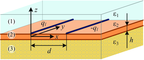
The geometry of the system is shown in Fig. 1. Two parallel wires with opposite linear charge densities, , are located on top of the ferroelectric film. The distance between the wires, , is much larger than their radius, , and the film thickness, . We also account for anisotropy of the film, assuming that the in-plane (transverse) dielectric constant differs from the out-of-plane (longitudinal) one, , by the anisotropy factor and is equal to . The origin of the rectangular coordinate system is selected in the middle of the film, just below the left wire. The -axis is directed perpendicular to the film plane, the -axis is directed along the wires and the -axis is perpendicular to them. Thus, left and right wires have the coordinates and correspondingly. The translational symmetry of this system in -direction permits to reduce the consideration to the 2D space, .
3 Method
Using the methods of electrostatics we calculate the distribution of the electrostatic potential induced by one of the wires (left one). The corresponding Poisson equations have to be written separately for each constituent part of the system (Fig. 1), the external environment space (region 1), film (2) and substrate (3) :
| (1) |
where is the charge distribution of the wire. The electrostatic boundary conditions are applied at the interfaces between the regions. We set and for the located at environment - film interface, (1)-(2), and and for the located at film - substrate interface, (2)-(3).
| a) | b) |
The Fourier method, similar to the one applied in [12, 13] for point charges, is used to solve the system (1) and find the relevant asymptotes. Following this method, the cos-Fourier transform of the potential inside the film, , is found as:
| (2) |
Here, is a characteristic length of the system,
| (3) |
that will be used below to delimit the regions with a different spatial decay of in the -direction. The inverse transformation of Eq. (2),
| (4) |
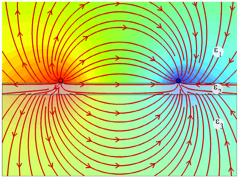
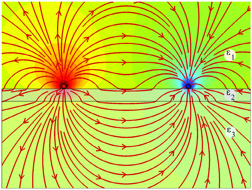
permits to find the expression for . Similar calculations can be done for and . The results of the numerical solution of Eqs. (1) for two typical sets of dielectric constants , and are presented in Fig. 2.
4 Results
Having calculated the potential induced by one of the wires and taking into account their equivalence we can find the capacitance of the system per unit of length as where is the potential difference between the wires. For the large wire separation, , the first term in contributes as the -independent cutoff constant, whereas the second one can be calculated analytically, by an expansion of (2) in series over the small parameter that allows for exact integration in Eq. (4). Finally, we obtain the following expression for the inverse capacitance,
| (5) |
where is the non-essential for further analysis constant that comprises the wire-scale cut-off,
| (6) |
and
| (7) |
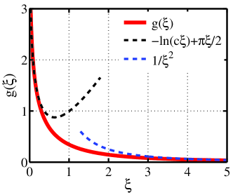
is the shown in Fig. 3 auxiliary function composed from the Sine and Cosine Integrals [14].
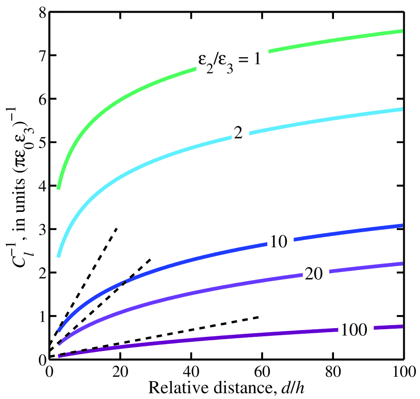
Given by Eq. (5) dependence of the system capacitance on the distance between the wires presents the basic result for determination of the dielectric constant of the film that enters there through two fitting parameters, and . We discuss now in detail how this procedure can be implemented in practice, considering for simplicity the isotropic film with , encompassed by the external environment with that gives and . We analyze separately the cases of high- and low- films (with and correspondingly) that have different electrostatic behavior. As shown in Fig. 2, wires-induced electric field lines are “repelled” from the film in the first case (Fig. 2,a) and “captured” by the film in the second one (Fig. 2,b). Fig. 4 presents given by Eq. (2) dependence of the inverse capacitance , measured in units m/pF, on the relative distance between the wires, , for both cases.

| a) | b) |
High- film, .
For a large ratio the characteristic scale can be comparable and even larger than the linear size of the system, and therefore the -function can be expanded over the small parameter as [14], (Fig. 3), where is the Euler’s constant, . Then, the resulting expression for can be simplified to:
| (8) |
that permits to measure via the linear slope of dependence at (Fig. 4,a). This method is analogous to that for geometry of planar capacitor with semi-infinite plates [10] due to the similar linear dependence on the distance between electrodes. Presented in Fig. 4,a numerical analysis shows, however, some restrictions for the application of this method. The distance between electrodes at which the linearity is manifested should be rather small (but still larger than and ) and the parameter should be large enough.
Low- film, .
For small the opposite situation, , takes place and the large-scale approximation for the -function can be used, [14]. Then, Eq. (5) is simplified to:
| (9) |
the corresponding dependencies being shown in Fig. 4,b.
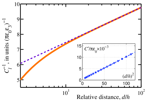
To extract the value of from experimental data one should first get rid of the -independent contribution presented by the logarithmic term in Eq. (9), which contains the unknown cut-off constant. For this, one can plot in units vs. as shown in Fig. 5 and subtract the linear background, manifested at . The residual contribution to the capacitance, , is given by the simple dependence , independent of the value of . Then, the dielectric constant, , can be extracted from the slope of , plotted in units as a function of (Inset to Fig. 5).
Note that for the low- films the small ratio can be realized only for the distances much smaller than the cutoff lengths, and . Therefore the linear approximation over , used in [10], makes no sense here.
5 Conclusion
The explicit analytical expression (5) derived for the capacitance of two parallel wires placed on top of the substrate-deposited film gives a way for experimental non-destructive measurements of the dielectric constant of this film. For experimental implementation, it can be convenient to deposit the system of equidistant wires and measure consequently the capacitance between them. The technical procedure consists in the determination of the capacitance as a function of the distance between the wires with subsequent comparison (fit) with functional dependence, given by Eq. (5). Simple and intuitively clear realizations of this method for high- and low- films (with respect to substrate) are proposed. The suggested procedure is based on the exact expression that permits to measure the dielectric constant for those systems in which traditionally used techniques are less precise or even fail because of the uncontrolled approximations.
We acknowledge the stimulating discussions with T. Baturina, V. Vinokur and A. Razumnaya. This work was supported by FP7-ITN-NOTEDEV project.
References
- [1]
- [2] D. Shi, Functional thin films and functional materials: new concepts and technologies (Springer Science & Business Media, 2003).
- [3] A. Lakhtakia and R. Messier, Sculptured thin films: nanoengineered morphology and optics (SPIE press Bellingham, WA, 2005).
- [4] R. Ramesh and N. A. Spaldin, Nature materials 6(1), 21–29 (2007).
- [5] S. Zhang, Nanostructured thin films and coatings: mechanical properties (CRC Press, 2010).
- [6] G. Hass, M. H. Francombe, and R. W. Hoffman, Physics of Thin Films: Advances in Research and Development (Elsevier, 2013).
- [7] G. Chatzigeorgiou, A. Javili, and P. Steinmann, Philosophical Magazine 95(28-30), 3402–3412 (2015).
- [8] R. Shao, S. V. Kalinin, and D. A. Bonnell, Applied Physics Letters 82(12), 1869–1871 (2003).
- [9] G. Gomila, J. Toset, and L. Fumagalli, Journal of Applied Physics 104(2), 024315 (2008).
- [10] O. Vendik, S. Zubko, and M. Nikol’skii, Technical Physics 44(4), 349–355 (1999).
- [11] A. Deleniv, Technical Physics 44(4), 356–360 (1999).
- [12] N. Rytova, Vestnik MSU (in Russian) 3, 30–37 (1967).
- [13] T. I. Baturina and V. M. Vinokur, Annals of Physics 331, 236–257 (2013).
- [14] M. Abramowitz, I. A. Stegun, and R. H. Romer, American Journal of Physics 56(10), 958–958 (1988).