Negative Kerr nonlinearity of graphene
as seen via chirped-pulse-pumped self-phase modulation
Abstract
We experimentally demonstrate a negative Kerr nonlinearity for quasi-undoped graphene. Hereto, we introduce the method of chirped-pulse-pumped self-phase modulation and apply it to graphene-covered silicon waveguides at telecom wavelengths. The extracted Kerr-nonlinear index for graphene equals m2/W. Whereas the sign of turns out to be negative in contrast to what has been assumed so far, its magnitude is in correspondence with that observed in earlier experiments. Graphene’s negative Kerr nonlinearity strongly impacts how graphene should be exploited for enhancing the nonlinear response of photonic (integrated) devices exhibiting a positive nonlinearity. It also opens up the possibility of using graphene to annihilate unwanted nonlinear effects in such devices, to develop unexplored approaches for establishing Kerr processes, and to extend the scope of the “periodic poling” method often used for second-order nonlinearities towards third-order Kerr processes. Because of the generic nature of the chirped-pulse-pumped self-phase modulation method, it will allow fully characterizing the Kerr nonlinearity of essentially any novel (2D) material.
I Introduction
The emergence of graphene, a 2D honeycomb lattice of carbon atoms with a linear electronic band structure, has had an enormous impact on numerous research areas, including that of nonlinear optics. Already in 2010 Hendry and co-workers found the Kerr nonlinearity of graphene 111We here refer to the parametric Kerr effect, which differs from the non-parametric saturable absorption effect in graphene to be extremely strong – a direct result from the material’s unique band structure – Hendry , and this experimental observation attracted much attention from the broad community working on advanced Kerr-nonlinear light generation phenomena such as supercontinuum and frequency-comb generation Holzwarth ; Kippenberg ; Savage . To extract graphene’s Kerr nonlinearity, Hendry et al. used “free-space” laser excitation to establish four-wave mixing (FWM) in a graphene sample, and later on also free-space Z-scan measurements Kockaert were employed for this purpose. Meanwhile, the ever-increasing importance of integrated photonics encouraged researchers to combine graphene’s nonlinear optical properties with on-chip (semiconductor) waveguide structures Gu ; Zhou ; Ji ; Hu . Covering a waveguide with graphene dramatically changes the waveguide’s nonlinear behavior because of the interaction between the evanescent tails of the guided mode and the 2D top layer. Despite graphene’s very strong Kerr nonlinearity as was already demonstrated in 2010, a rather limited number of on-chip nonlinear-optical graphene devices have been reported on so far, and they mostly rely on FWM in graphene-covered silicon waveguides Gu ; Zhou ; Ji ; Hu . To pave the way to a more varied exploitation of graphene in nonlinear photonic integrated circuits and enable advanced nonlinear light generation, not only the strength or magnitude of graphene’s Kerr nonlinearity has to be known but also its sign needs to be measured, since the latter determines whether the nonlinear effects induced by the graphene and the underlying waveguide add or subtract. The Kerr coefficient of the graphene cover layer has been (tacitly) assumed to be positive in the demonstrated FWM devices, but in fact FWM intrinsically only allows measuring the coefficient’s magnitude and not its sign. If with another method one can also assess the sign, this knowledge will enable researchers to fully exploit graphene’s promise as efficiency-enhancing material in essentially any nonlinear photonic system. In this article, we examine both the magnitude and the sign of graphene’s Kerr nonlinearity using a different approach, namely by means of chirped-pulse-pumped self-phase modulation (SPM) experiments in graphene-covered silicon waveguides.
II Basic principles of chirped-pulse-pumped SPM
The following explanation on the physics of the chirped-pulse-pumped SPM approach shows that, as opposed to FWM experiments, it does enable assessing the sign of a material’s Kerr nonlinearity. SPM is a Kerr process that broadens or narrows the spectral width of an input laser pulse Agrawal ; Pinault . This broadening or narrowing effect can become very pronounced even at modest excitation powers, provided that the input pulse exhibits chirp. Let us consider a waveguide section of length in which a pulse propagates with amplitude . For a Fourier-transformed amplitude centered at frequency , the square of the spectral width can be written as Pinault ; CastelloLurbe , which in the time domain can be expressed as Pinault . For the experiments reported in this Letter, the pulse propagation is mostly determined by Kerr-nonlinear effects rather than dispersion and free-carrier effects (which was also verified numerically with the inclusion of graphene-generated free carriers CastelloLurbe ; Vermeulen ). Hence, we can adopt a simplified version of the nonlinear Schrdinger equation incorporating only SPM effects and linear loss: , with the Kerr nonlinearity and the linear loss coefficient. This yields:
| (1) |
where represents the effective length. When rewriting as with the input peak power, implementing Eq. (1) in results in the following expression for the relative spectral broadening factor after propagation over :
| (2) |
with being the input pulse shape factors:
| (3) |
When assuming a quadratic input phase profile with input chirp parameter , Eq. (2) yields:
| (4) |
with the new dimensionless shape factors all having positive values determined by:
| (5) | ||||
For a Gaussian pulse with exp and a sech2 pulse with sech, these shape factors become, respectively: and ; and ; and . We point out that for only the term containing remains, and the formula reported in Pinault is recovered.
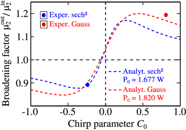
Eq. (4) in fact corresponds to earlier presented SPM formulas Agrawal ; Pinault , while also taking into account the input chirp parameter. In the high-power regime, the term proportional to in Eq. (4) will be dominant, and the broadening factor will be larger than 1 with the highest value attained at , i.e. for a transform-limited input pulse Boyraz . At low powers, however, the term proportional to becomes important, and depending on the sign of 222We point out that for temporal pulse broadening or narrowing in a waveguide with dispersion , the sign of plays an analogous role Agrawal , the broadening factor can either be larger or smaller than 1 (i.e. one has either broadening or narrowing), with a maximum or minimum value at a non-zero chirp. As such, when exciting a waveguide with a moderate-power pulse exhibiting an appropriately chosen chirp , the nature of the spectral width modification, i.e. broadening or narrowing, will indicate the sign of the waveguide’s Kerr nonlinearity . This is also illustrated in Fig. 1 depicting the spectral broadening factor of Eq. (4) as a function of for a silicon waveguide (see further on), the Kerr nonlinearity of which is known to be positive at wavelengths above nm Bristow . In Fig. 1 the spectral broadening and narrowing obtained at, respectively, substantially positive and negative -values indeed unambiguously demonstrate the positive sign of silicon’s Kerr nonlinearity 333In the low-power regime, spectral broadening can also be obtained at a negative input chirp (see centre region of Fig. 1), provided that the chirp value is sufficiently close to zero to let the last term in Eq. (4) dominate.. In a similar way, by carrying out chirped-pulse-pumped SPM experiments with graphene-covered silicon waveguides and factoring out silicon’s nonlinear response, we can determine the sign of graphene’s Kerr nonlinearity.
III Experimental setup and results
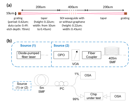
To perform such chirped-pulse-pumped SPM experiments, we employed grating-coupled bare and graphene-covered silicon-on-insulator (SOI) waveguide structures designed for operation around the nm telecom wavelength, and all featuring the same layout for the gratings, tapers and the actual waveguide section (see Fig. 2(a)). The waveguide’s cross-section has a width of nm and a height of nm which is standard for SOI chips fabricated by ePIXfab epixfab . Because of the identical layouts of the bare and graphene-covered SOI waveguides, the bare waveguide can serve as a reference structure with a well-known Kerr nonlinearity magnitude and sign at nm. We also considered this waveguide for plotting the theoretical broadening factor in Fig. 1, where we applied the model of Eq. (4) to the taper and waveguide sections in a cascaded way. Hereto, we used dB/cm and W-1mm-1 CastelloLurbe in the waveguide section, and we assumed a scaling of these parameters inversely proportional with the waveguide width in the tapered sections. The graphene deposition on the waveguides has been described in our earlier work VanErps . Chemical-vapor-deposition-grown graphene was transferred on the SOI chip, inducing a high linear waveguide loss of dB/cm at nm, and the layer was patterned to vary the length of the graphene sections on top of the waveguides VanErps . The Fermi energy of the graphene sheet was about eV as a result of weak unintentional doping induced by the transfer process itself Ciuk , so that at nm we were operating in graphene’s high-loss regime above its single-photon absorption threshold.
We carried out SPM measurements for both a positive and negative input chirp using the experimental setup shown in Fig. 2(b). The pulsed laser sources used to excite the waveguides were a diode-pumped fiber laser (Calmar FPL-02CTF-POL; Source (1) in Fig. 2(b)) and a fiber-coupled optical parametric oscillator or OPO (APE Levante IR with a variable optical attenuator or VOA; Source (2)) generating, respectively, Gaussian pulses at a repetition rate of MHz and sech2 pulses at a repetition rate of MHz. The pulses were coupled into and out of the waveguides by means of flat-cleaved fiber probes positioned above the waveguides’ grating couplers at an angle of with respect to the vertical axis. We ensured excitation of the Transverse Electric (TE) mode in the waveguides using a fiber-based polarization controller (PC). To monitor the input spectrum, a 99:1 coupler was inserted in the setup to split off of the laser power towards a fiber-coupled optical spectrum analyzer or OSA (Yokogawa AQ6370D) just in front of the incoupling fiber probe. Simultaneously with the input spectrum, the output spectrum was measured with a second fiber-coupled optical spectrum analyzer just behind the outcoupling fiber probe. Prior to the SPM measurements, we measured the pulses’ temporal characteristics by means of a frequency-resolved optical gating (FROG) instrument (Coherent Solutions HR150). The actual SPM measurements consisted of simultaneously recording the spectral widths of the input and output spectra for the waveguides with graphene lengths varying from to m in steps of m.
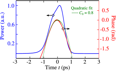
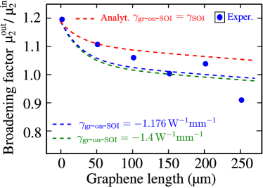
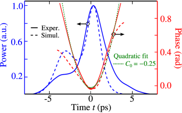
For the experiments with a positive input chirp, we employed the diode-pumped fiber laser set at an operation wavelength of nm, with the laser pulses guided over m of G.652 single-mode fiber (SMF) towards the waveguides. The measured temporal power and phase profiles as shown in Fig. 3 yield a full-width-at-half-maximum pulse length ps and a fitted chirp parameter . The latter was extracted from the quadratically fitted phase profile indicated as the dotted line in Fig. 3. The peak power coupled into the waveguide was set at W. The measured broadening factors as a function of the graphene length on top of the waveguides are depicted in Fig. 4. Since the input pulses were positively chirped, we observed for the bare SOI waveguide (graphene length of m) with spectral broadening as expected. The measured broadening factor lies closely to the corresponding theoretical value at in Fig. 1. The latter shows that the simple theory of Eq. (4) without inclusion of two-photon absorption or free-carrier effects is an adequate model for our experiments with modest peak powers, relatively short pulse durations and short waveguide lengths. For the SOI waveguides covered with graphene, the level of spectral broadening is reduced with increasing graphene length, and for sufficiently long graphene sections even spectral narrowing is observed. We point out that, since the graphene cover layers are situated in the centre of the m-long waveguide sections VanErps , all waveguides have an uncovered SOI section at the input with establishing spectral broadening. As shown in Fig. 4, this broadening is progressively counteracted by the graphene-covered sections, which consequently feature . This observation also showcases that depositing graphene on another nonlinear material will not always enhance the nonlinear response of the material system and in some cases even annihilates its nonlinear behavior.
The latter finding was also confirmed in our experiments with a negative input chirp. Hereto, we employed the OPO source tuned to a wavelength of nm. The pulses at the free-space output of the OPO are slightly positively chirped, but when coupled into a G.652 fiber with an appropriately chosen length, a negative pulse chirp can be obtained at the output of the fiber. Indeed, during propagation in the fiber, the pulses initially experience spectral broadening due to SPM effects in the fiber. At the same time, they are compressed in time due to the negative group velocity dispersion () of G.652 single-mode fiber in the telecom window around nm. As such, after having traveled a certain propagation distance, the pulses become transform-limited (), and beyond this point, they acquire a negative chirp induced by the fiber’s negative Agrawal . Based on numerical simulations, we found that ps-long OPO pulses with a peak power of W at the fiber input would reach this regime of negative chirp at a propagation distance of around m. Fig. 5 shows both the measured and numerically simulated temporal power and phase profiles at the output of a m-long fiber, as well as the quadratic fit of the experimental phase. The pulse length and chirp parameter are found to be ps and , respectively. The peak power that was coupled into the chip was set at W. Fig. 6 shows the measured broadening factors as a function of the graphene length on top of the waveguides. In view of the negative input chirp, we observed for the bare waveguide with spectral narrowing, with again a very good match between the measured spectral narrowing and the corresponding theoretical value at in Fig. 1. For the waveguides with graphene on top, we found that this narrowing is progressively counteracted by the graphene-covered sections exhibiting .
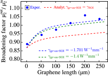
Besides extracting the sign of in the graphene-covered waveguide sections, we also evaluated its magnitude by fitting our model with the data points of Figs. 4 and 6, while using only as a fitting parameter. In this case, we used the more generalized model of Eq. (2) rather than Eq. (4), and again applied it to both the taper and waveguide sections in a cascaded way. Optimal fitting is achieved by minimizing the fitting error with the number of data points, and with the experimental and theoretical broadening factors, respectively. For Figs. 4 and 6, the optimal fitting was obtained for two very large, yet different nonlinearity values: W-1 mm-1 yielding , and W-1 mm-1 yielding , respectively. However, their average, W-1 mm-1 444The tolerance interval is calculated using the same formula as for the fitting error but with the two optimum fitting values and their average., yields an equally high-quality fitting of the experimental data. Indeed, using W-1 mm-1 results in approximately the same fitting error as when employing the two different nonlinearity values ( vs. 0.043 for Fig. 4 and vs. 0.022 for Fig. 6) 555Also when measuring the broadening factor as a function of input peak power instead of graphene length, we extracted the same value for .. In contrast, a poor fitting is obtained when assuming the graphene-covered waveguide sections to exhibit the same nonlinearity as the bare waveguide (i.e. ), which showcases the strong nonlinear impact of the graphene cover layer.
IV Extracting the Kerr nonlinearity of graphene
From the value W-1 mm-1 obtained for the effective Kerr nonlinearity in the graphene-covered waveguide sections, we can extract the nonlinearity of the graphene sheet itself using our earlier presented weighted-contributions formalism for hybrid waveguides Vermeulen . Starting from the actual waveguide mode profile in the presence of the graphene top layer and the corresponding propagation characteristics, this formalism, included in Appendix, calculates the weighted nonlinearity contributions of the graphene cover layer and of the underlying silicon material to the effective nonlinearity . Since is the parameter that we derived from the experiments, and since we can readily calculate the weighted nonlinearity contribution of the silicon waveguide, the formula in Appendix allows extracting the nonlinearity of the graphene layer itself. This is done in two steps: first, from the formula we derive that, as most of the modal power resides in the silicon material, the contribution of the silicon to W-1 mm-1 is given by of the bare waveguide, and that of the graphene cover layer equals W-1mm-1. Secondly, by assessing specifically the expression for the graphene contribution (i.e. the second term in the formula in Appendix), we then extract that the graphene sheet as an isolated material features a Kerr-nonlinear index of about m2/W or a susceptibility around . Its magnitude is in line with earlier reported graphene nonlinearity values Hendry ; Gu but the negative sign was not accounted for in those experiments. We point out that our earlier presented calculations for the Kerr nonlinearity of graphene Cheng1 ; Cheng2 ; Cheng3 , although underestimating its absolute value, do predict a negative sign for the nonlinearity of quasi-undoped graphene at optical wavelengths, both in the ideal case of zero electron scattering and in case of considerable inter- and intra-band scattering. The calculations show a negative Kerr nonlinearity resonance at the single-photon absorption threshold, and the negative nonlinearity sign persists also far above this threshold.
V Conclusion
In conclusion, using the chirped-pulse-pumped SPM method introduced here – a generic method that allows extracting both the magnitude and sign of the Kerr nonlinearity of any novel (2D) material Castellanos –, we have demonstrated a negative Kerr nonlinearity for quasi-undoped graphene, whereas the magnitude of the obtained value is in line with earlier experimental reports. Our findings imply that, when using graphene to enhance the nonlinear response of a photonic device or integrated circuit with a positive nonlinearity, one needs to carefully study how the 2D material should be implemented to actually achieve a net enhancement. Our results also show that, when targeting the compensation of unwanted nonlinearities in such a device or circuit, graphene could be of use as well. Finally, graphene’s negative Kerr nonlinearity can give rise to unexplored approaches for establishing Kerr interactions and even extend the scope of e.g. the “periodic poling” method often used for second-order nonlinearities Hum towards third-order Kerr processes.
*
Appendix A Weighted-contributions formalism
Below we briefly summarize the basic concepts of the weighted-contributions formalism used for extracting the graphene nonlinearity from the measured effective nonlinearity; for further details about this formalism we refer to Vermeulen . When assuming a graphene-covered silicon waveguide oriented along the direction, we can write the electric field associated with a waveguide mode as proportional to , where indicates the mode profile excited by the pump laser used; we assume the normal to the top of the waveguide to be . When determining this modal field using mode solver software, we incorporate the linear optical properties of silicon (assumed lossless at the wavelength of interest), and treat the graphene layer as a thin sheet with thickness on top of the waveguide. We employ the function () to indicate where the silicon (graphene) is situated; () where the silicon (the thin layer modeling the graphene) is present and () where the silicon (the thin layer modeling the graphene) is absent. We obtain the following formula for the effective Kerr nonlinearity measured in the self-phase modulation experiments with the graphene-covered silicon waveguides:
with and the weighted nonlinearity contributions from the underlying SOI waveguide and the graphene top layer, respectively. and are scaling factors defined in Vermeulen , is the dielectric permittivity, is the pump frequency, represents the third-order Kerr-nonlinear susceptibility of silicon, and is the third-order Kerr-nonlinear conductivity of graphene. The latter can be converted to a susceptibility using Cheng1 .
Acknowledgements.
This work was supported by the ERC-FP7/2007-2013 grant 336940, the EU-FET GRAPHENICS project 618086, the Hercules-stichting grant UABR/007/09, the FWO project G.A002.13N, the EU-FP7 Graphene Flagship 604391, VUB-OZR, BELSPO-IAP, and Methusalem.References
- (1) E. Hendry, P. J. Hale, J. Moger, A. K. Savchenko, and S. A. Mikhailov, Coherent Nonlinear Optical Response of Graphene, Phys. Rev. Lett. 105, 097401 (2010).
- (2) R. Holzwarth, T. Udem, T. W. Hansch, J. C. Knight, W. J. Wadsworth, and P. S. J. Russell, Optical Frequency Synthesizer for Precision Spectroscopy, Phys. Rev. Lett. 85, 2264 (2000).
- (3) T. J. Kippenberg, R. Holzwarth, and S. A. Diddams, Microresonator-Based Optical Frequency Combs, Science 332, 555 (2011).
- (4) N. Savage, Supercontinuum sources, Nat. Phot. 3, 114 (2009).
- (5) H. Zhang, S. Virally, Q. Bao, L. K. Ping, S. Massar, N. Godbout, and P. Kockaert, Z-scan measurement of the nonlinear refractive index of graphene, Opt. Lett. 37, 1856 (2012).
- (6) T. Gu, N. Petrone, J. F. McMillan, A. van der Zande, M. Yu, G. Q. Lo, D. L. Kwong, J. Hone, and C. W. Wong, Regenerative oscillation and four-wave mixing in graphene optoelectronics, Nat. Phot. 6, 554 (2012).
- (7) H. Zhou, T. Gu, J. F. McMillan, N. Petrone, A. van der Zande, J. C. Hone, M. Yu, G. Lo, D.-L. Kwong, G. Feng, S. Zhou, and C. W. Wong, Enhanced four-wave mixing in graphene-silicon slow-light photonic crystal waveguides, Appl. Phys. Lett. 105, 091111 (2014).
- (8) M. Ji, H. Cai, L. Deng, Y. Huang, Q. Huang, J. Xia, Z. Li, J. Yu, and Y. Wang, Enhanced parametric frequency conversion in a compact silicon-graphene microring resonator, Opt. Express 23, 18679 (2015).
- (9) X. Hu, Y. Long, M. Ji, A. Wang, L. Zhu, Z. Ruan, Y. Wang, and J. Wang, Graphene-silicon microring resonator enhanced all-optical up and down wavelength conversion of QPSK signal, Opt. Express 24, 7168 (2016).
- (10) G. P. Agrawal, Nonlinear Fiber Optics (Academic Press, 4th ed., 2007).
- (11) S. C. Pinault and M. J. Potasek, Frequency broadening by self-phase modulation in optical fibers, J. Opt. Soc. Am. B 2, 1318 (1985).
- (12) D. Castelló-Lurbe and E. Silvestre, Supercontinuum generation in silicon waveguides relying on wave-breaking, Opt. Express 23, 25462 (2015).
- (13) N. Vermeulen, J. L. Cheng, J. E. Sipe, and H. Thienpont, Opportunities for wideband wavelength conversion in foundry-compatible silicon waveguides covered with graphene, IEEE J. Sel. Top. Quantum Electron. 22, 8100113 (2016).
- (14) O. Boyraz, T. Indukuri, and B. Jalali, Self-phase-modulation induced spectral broadening in silicon waveguides, Opt. Express 12, 829 (2004).
- (15) A. D. Bristow, N. Rotenberg, and H. M. van Driel, Two-photon absorption and Kerr coefficients of silicon for 850–2200 nm, Appl. Phys. Lett. 90, 191104 (2007).
- (16) http://www.epixfab.eu/
- (17) J. Van Erps, T. Ciuk, I. Pasternak, A. Krajewska, W. Strupinski, S. Van Put, G. Van Steenberge, K. Baert, H. Terryn, H. Thienpont, and N. Vermeulen, Laser ablation- and plasma etching-based patterning of graphene on silicon-on-insulator waveguides, Opt. Express 23, 26639 (2015).
- (18) T. Ciuk, I. Pasternak, A. Krajewska, J. Sobieski, P. Caban, J. Szmidt, and W. Strupinski, Properties of Chemical Vapor Deposition Graphene Transferred by High-Speed Electrochemical Delamination, J. Phys. Chem. C 117, 20833 (2013).
- (19) J. L. Cheng, N. Vermeulen, and J. E. Sipe, Third order optical nonlinearity of graphene, New J. Phys. 16, 053014 (2014).
- (20) J. L. Cheng, N. Vermeulen, and J. E. Sipe, Third-order nonlinearity of graphene: Effects of phenomenological relaxation and finite temperature, Phys. Rev. B 91, 235320 (2015).
- (21) J. L. Cheng, N. Vermeulen, and J. E. Sipe, Numerical study of the optical nonlinearity of doped and gapped graphene: From weak to strong field excitation, Phys. Rev. B 92, 235307 (2015).
- (22) A. Castellanos-Gomez, Why all the fuss about 2D semiconductors?, Nat. Phot. 10, 202 (2016).
- (23) D. S. Hum and M. M. Fejer, Quasi-phasematching, C. R. Physique 8, 180 (2007).