Strain in epitaxial MnSi films on Si(111) in the thick film limit studied by
polarization-dependent extended x-ray absorption fine structure
Abstract
We report a study of the strain state of epitaxial MnSi films on Si(111) substrates in the thick film limit (100-500 Å) as a function of film thickness using polarization-dependent extended x-ray absorption fine structure (EXAFS). All films investigated are phase-pure and of high quality with a sharp interface between MnSi and Si. The investigated MnSi films are in a thickness regime where the magnetic transition temperature assumes a thickness-independent enhanced value of 43 K as compared with that of bulk MnSi, where . A detailed refinement of the EXAFS data reveals that the Mn positions are unchanged, whereas the Si positions vary along the out-of-plane [111]-direction, alternating in orientation from unit cell to unit cell. Thus, for thick MnSi films, the unit cell volume is essentially that of bulk MnSi — except in the vicinity of the interface with the Si substrate (thin film limit). In view of the enhanced magnetic transition temperature we conclude that the mere presence of the interface, and its specific characteristics, strongly affects the magnetic properties of the entire MnSi film, even far from the interface. Our analysis provides invaluable information about the local strain at the MnSi/Si(111) interface. The presented methodology of polarization dependent EXAFS can also be employed to investigate the local structure of other interesting interfaces.
I Introduction
Skyrmions are topologically non-trivial whirls of the magnetization. They have been observed as individual objects as well as in the form of periodic, three-dimensional lattices with periodicities in the range , covering nearly two orders of magnitude.Mühlbauer et al. (2009); Pfleiderer et al. (2010); Nagaosa and Tokura (2013a) Magnetic skyrmions were first identified in bulk compounds with non-centrosymmetric crystal structure, such as the B20 family of crystals, in which the Dzyaloshinskii-Moriya spin-orbit interactions play a crucial role. Using small angle neutron scattering,Mühlbauer et al. (2009); Adams et al. (2011) and magnetotransport measurements (topological Hall effect),Neubauer et al. (2009) the non-trivial topological character of the skyrmion lattice could be confirmed. However, it was in particular the observation that skyrmions in bulk samples can be easily manipulated with current densities that are nearly six orders of magnitude smaller than those needed for conventional spin transfer torque (STT) based schemes (currently 1011 A m-2) that has generated great interest in skyrmions as a novel route towards applications.Jonietz et al. (2010)
First studies in thinned bulk samples using real space imaging by means of Lorentz transmission electron microscopy (LTEM) early on suggested that skyrmions tend to be favored in systems of reduced size.Yu et al. (2010, 2011); Tonomura et al. (2012) In addition, skyrmions have also been detected by means of spin-resolved scanning tunneling microscopy in thin films grown on carefully selected substrates mediating strong antisymmetric spin interactions.Heinze et al. (2011)
For future applications such as skyrmionic memory and logic devices,Zhang et al. (2015) the development of skyrmion-carrying thin films and nanomaterials on common semiconductor substrates is a crucial prerequisite.Nagaosa and Tokura (2013b) As the non-centrosymmetric B20 phase of MnSi is among the most extensively studied skyrmion systems, thin films on a Si substrate appear to be an obvious choice — at least for studies of fundamental aspects.Mühlbauer et al. (2009); Jonietz et al. (2010); Milde et al. (2013); Nagaosa and Tokura (2013a); Schwarze et al. (2015) In fact, the skyrmion lattice phase is not only observed in MnSi bulk crystals, but also in many other Si- and Ge-based B20 systems that are helimagnetically ordered in zero magnetic field, such as Fe1-xCoxSi,Münzer et al. (2010) Mn1-xFexSi, Mn1-xCoxSi,Pfleiderer et al. (2010) and related Ge-based compounds.
Phase-pure MnSi films on Si(111) have been successfully grown by molecular beam epitaxy (MBE).Karhu et al. (2010, 2011, 2012); Wilson et al. (2012, 2013); Li et al. (2013); Menzel et al. (2013); Wilson et al. (2014); Yokouchi et al. (2015); Zhang et al. (2016) Yet, despite of the high quality of the films reported in the literature, it is still unresolved if a skyrmion lattice phase forms in MnSi epilayers.Meynell et al. (2014) A first important difference between thin bulk samples and epilayers concerns the helimagnetic transition temperature, which is reduced from 30 K to 25 K in the former, whereas increased values as high as 80 K are consistently observed for thin films on Si(111).Zhang et al. (2016)
Further, for the applied magnetic field perpendicular to the epitaxial films, early polarized neutron reflectometry and magnetization measurements, eventually led to the conclusion that skyrmions do not form. This was challenged by LTEM studies and Hall effect measurements,Li et al. (2013) which initially appeared to provide putative evidence for skyrmions, but eventually seemed to confirm the absence of skyrmions.Meynell et al. (2014) In contrast, for the magnetic field parallel to the film, it has been suggested that skyrmion cigars form as conjectured from magnetization measurements as well as recent studies of the planar Hall effect.
In view that individual skyrmions as well as skyrmion-lattice order have been observed in thinned bulk samples with a thickness comparable to MBE-grown epilayers, the interface with the Si substrate must be an important source for the differences of the magnetic properties of bulk samples and epilayers.
It is conceivable that the interface may thereby influence the properties of the thin films in at least two prominent ways. First, it has recently been suggested theoretically, that the mere existence of a surface already generates additional terms in the free energy that modify the magnetic order within a considerable distance to the interface.Müller et al. (2016) Second, the lattice mismatch generates strain and it is the response to this strain that drives modifications of the magnetic properties.Wilson et al. (2014)
Two variants of lattice strain may be distinguished, notably isotropic strain as generated by hydrostatic pressures and anisotropic strain generated by uniaxial compressive or tensile pressures. The former has long been explored in great detail in bulk samples, where a suppression of the helimagnetic transition temperature is observed, and more recently in thin films.Engelke et al. (2014) In contrast, the effects of uniaxial pressure have only been investigated recently in detail for bulk MnSi using small-angle neutron scattering.Chacon et al. (2015); Nii et al. (2015)
In order to resolve the controversies surrounding the magnetic phases in epitaxial MnSi thin films on Si(111) a first and important step are detailed measurements of the in-plane and out-of plane lattice parameters of the films. In particular, this represents a precondition for strain engineering of thin films with higher transition temperatures and tailored skyrmion lattices.Zhang et al. (2016)
For our study we used extended x-ray absorption fine structure (EXAFS) to determine the local atomic environment of Mn atoms in MnSi thin films on Si(111) in order to infer the presence and size of local strain. EXAFS is a powerful tool for quantifying the variation of interatomic distances, which has been successfully used to study surface and interfaces structure in, e.g., MnSi monolayers.Kahwaji et al. (2012) The polarization dependence of the EXAFS cross-section allows for isolation of the contributions of the bonds along different directions. By exploiting the linear polarization of the synchrotron radiation and by orienting the sample with the surface normal either parallel or perpendicular to the electric vector of the impinging x-rays, it is possible to probe either the out-of-plane or in-plane atomic bonds. This analysis provides direct information about strain in well-oriented thin films such as MnSi on Si(111) and could be used to investigate other systems where the local strain at the interface affects their electronic and magnetic properties as in the case of superconducting latticesFogel et al. (2001); Tang and Fu (2014) or heterostructures incorporating topological insulators.Vobornik et al. (2011); Li et al. (2015) In the following we will describe our results on differently prepared MnSi thin films as a function of film thickness.
Our paper is organized as follows. Section II reviews the state of the art on the MnSi/Si(111) system as reported in the literature. As the evolution of the properties of epitaxial films of MnSi depend sensitively on the film thickness in the thin film limit, earlier work provides an important point of reference for our study of thick films reported here. In Sec. III we summarize the sample growth, pre-characterization of the thin films, and experimental details of our EXAFS measurements. Results of the polarization-dependent EXAFS measurements on two series of samples are presented and discussed in Sec. IV.1. Section IV.2 presents the refinement results allowing for an extraction of the relative movements of the atoms in the unit cell. The somewhat surprising main result of our EXAFS measurements concerns that the Mn positions in thick MnSi films are unchanged, whereas the Si positions vary along the out-of-plane [111]-direction, whereby the orientation reverses in adjacent unit cells. Thus, for thick MnSi films, the unit cell volume is essentially unchanged from that of bulk MnSi except in the vicinity of the interface with the Si substrate. In conclusion, the mere existence of an interface appears to affect the magnetic properties of thin film MnSi strongly as discussed in Sec. V.
II The MnSi/Si(111) system
In a series of seminal papers the details of epitaxial MnSi films on Si (111) have been explored in great detail for the thin film limit. Karhu et al. (2010, 2011); Engelke et al. (2012); Karhu et al. (2012); Wilson et al. (2012, 2013); Li et al. (2013); Menzel et al. (2013); Meynell et al. (2014); Wilson et al. (2014); Yokouchi et al. (2015); Engelke et al. (2014) The lattice parameter at room temperature of Si is Å, whereas that of B20 MnSi is Å. When grown on Si(111) with the epitaxial relationship Si(111) MnSi(111) and Si MnSi [cf., Fig. 2(a)], the lattice mismatch between MnSi(111) and Si(111), as determined by , is 3.0%.Karhu et al. (2010, 2012) This tensile strain represents a comparably large value and the formation of a dislocation network can be expected, still resulting in some residual strain. The defects have been identified as misfit edge dislocations with a Burgers vector of .Karhu et al. (2010, 2012)
In-plane and out-of-plane strain has been studied by various groups using, e.g., transmission electron microscopy (TEM) plane-view selected-area diffraction patternsKarhu et al. (2010, 2012) and density functional theory calculations.Geisler and Kratzer (2013) The studies focused on reactively grown MnSi layers and did not cover stoichiometrically grown films. The reactively grown films show an interesting increase of the out-of-plane strain with film thickness up to 70 Å, above which the strain reduces again. The in-plane strain, on the other hand, smoothly reduces as the films are grown thicker.Karhu et al. (2012) In MBE, MnAs films can be grown up to a thickness of 500 Å.Zhang et al. (2016)
The influence of strain on the magnetic transition temperature has been measured as a function of film thickness (see Fig. 6 in Ref. Karhu et al., 2010). At 70 Å, where the out-of-plane strain is at its maximum, the measured magnetic transition temperature coincides with the bulk value for MnSi. Above 100 Å, the value saturates at about 15 K above the bulk value. Figure 1 summarizes the structural properties of MnSi thin films on Si(111). In our films, which are grown by a combination of reactive seed layer formation and stoichiometric deposition, much higher transition temperatures were found.Zhang et al. (2016)
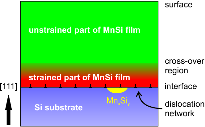
Given further that the electronic properties of Si do not appear to be essential for the formation of the skyrmions, the most prominent effect of the interface appears to be the occurrence of strain, affecting the delicate balance of the energy terms stabilizing the skyrmion phase. However, in order to clarify the precise mechanism causing the enhanced magnetic transition temperature detailed measurements of the structural properties of epitaxial MnSi film in the thick film limit are required as reported below.
III Materials System and Experimental Methods
III.1 Sample preparation and characterization
Epitaxial MnSi(111) thin films were grown by MBE on Si substrates measuring 10 12 cm2. The Balzers MBE system has a base pressure of mbar and is equipped with electron-beam evaporators and effusion cells. Flux control is achieved via cross-beam mass spectrometry. Prior to loading, the Si wafers were first degreased, followed by etching in hydrofluoric acid and oxidation by H2O2. Annealing at 990∘C, and growing a Si buffer layer, leads to the reconstruction, as confirmed by reflection high energy electron diffraction (RHEED). The sample is then cooled down to room-temperature and 3 monolayers (MLs) of Mn were deposited before they are reacted with the Si surface at an elevated temperature of 250-300∘C. (1 ML corresponds to atoms/cm2.) This leads to the formation of an epitaxial MnSi seed layer. The MnSi layer has a R30∘ structure [Fig. 2(c)], as determined by RHEED. The subsequent MnSi growth is by the stoichiometric supply of Mn and Si. The growth proceeds up to a thickness of roughly 500 Å without any signs of the formation of a secondary phase. It is worth noting that the surface of the seed layer prepared in this way (reactive epitaxy) is not perfect.Geisler et al. (2012) In fact, choosing the described Mn thickness and annealing conditions assures that the surface is as flat as possible. The in-vacuo study of freshly grown MnSi layer by scanning tunneling microscopy (STM) showed a large variation in surface morphology,Kumar et al. (2004) however, its effect on strain in the subsequent layer is not known in detail. Figure 1 summarizes the structural properties of the MnSi/Si(111) system as reported in the literature, and also includes our own findings in the thick film limit.
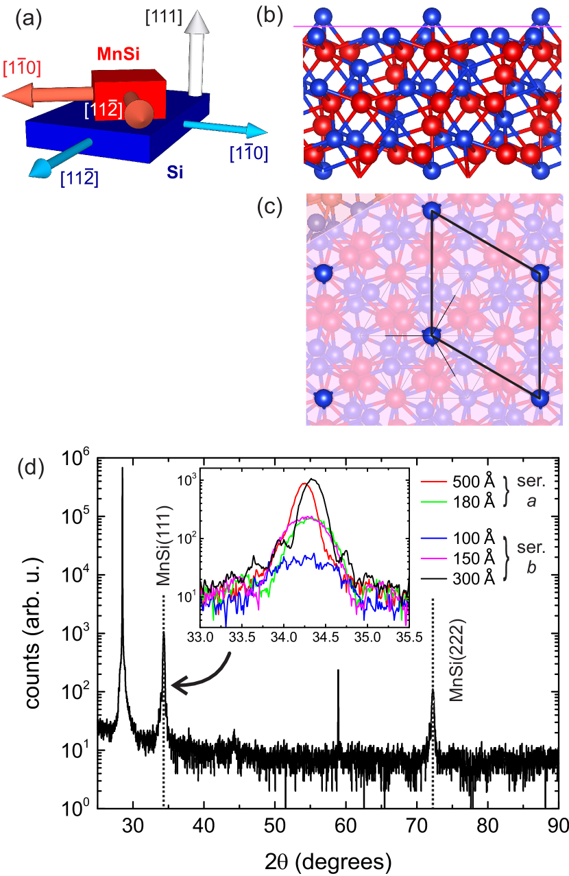
Two groups of samples were grown, namely with (series ) and without (series ) a Si buffer layer. Both series include different thicknesses, as confirmed by x-ray reflectivity, of 100, 150, 180, 300, and 500 Å, thereby covering the range from a couple of ML thick seed layers to the maximum achievable B20 phase film thickness. All films were characterized by XRD [Fig. 2(d)]. In order to protect the films from oxidation, a thin amorphous silicon cap was added to some of them.
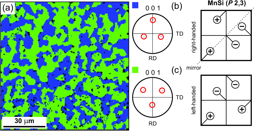
We found chiral domains in the films and visualized them using electron backscatter diffraction (EBSD) in an JEOL 6500F scanning electron microscope (SEM) fitted with an EBSD phosphor screen detector and CCD camera. The EBSD map of the 500-Å-thick MnSi film [Fig. 3(a)] shows that the chiral domains, which have a correlation length on the order of 10 m, are equally distributed.
The sample for cross-sectional TEM was prepared by mechanical polishing followed by Ar ion-beam milling. The high-resolution TEM phase-contrast image [Fig. 4(a)] indicates that the MnSi film is a highly ordered, epitaxial structure on the Si(111) substrate, and that the interface between substrate and film is sharp. The power spectra observed at different locations of the film [example shown in Fig. 4(b)] are identical and can be indexed to the B20 cubic MnSi phase (space group , nm) with a zone axis of [112]. The Si(111) substrate power spectrum is indexed as the diamond space group and the zone axis is identified as [110].
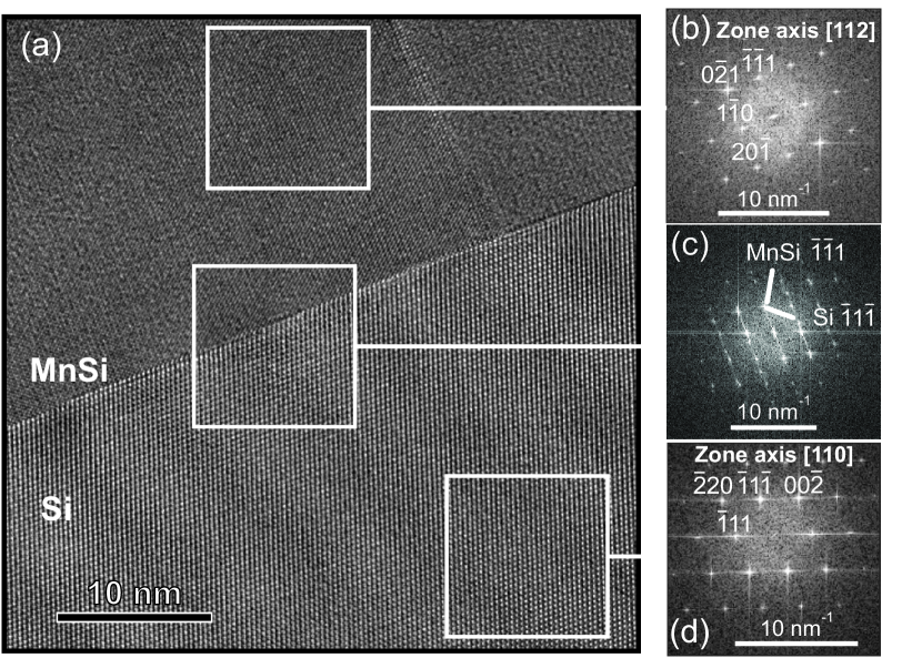
Another important fact is that the power spectra obtained at different locations of the Si substrate do not show a significant or dominant presence of other Mn-Si phases in the substrate.
Minor cases of inclusions were detected by TEM, as reported previously.Zhang et al. (2016)
The power spectrum calculated at the
interface between substrate and film [Fig. 4(d)] is a
combination of the power spectra from Si(111) and MnSi and it shows
that () planes of MnSi and ()
planes of the Si substrate are parallel. From these observations,
the epitaxial relationship between MnSi film and Si substrate can be
written as MnSi{111}112 Si{111}110.
III.2 EXAFS measurements and analysis
X-ray absorption near edge structure (XANES) and EXAFS spectra were collected at the Mn edge (6539 eV) of the thin film samples at room temperature on beamline B18 at the Diamond Light Source. Bulk MnSi in powder form and a Mn foil were measured as references. The powdered MnSi bulk was pressed into a pellet with the optimized quantity for measurements in transmission mode.
A nine-element solid-state Ge detector with digital signal processing for fluorescence detection was used to measure the thin films. The polarization dependence arises from the different geometries employed for data collection. Measurements were performed in two orientations of the films with respect to the polarization vector of the linearly polarized synchrotron radiation, so that this vector is aligned either parallel or perpendicular to the sample surface, i.e., at an incident angle of 10∘ [normal, with electric field vector E of the x-rays nearly parallel to the MnSi(111) plane] and 80∘ [grazing, with E nearly perpendicular to the MnSi(111) plane], c.f. Fig. 2(a). All spectra were acquired in quick-EXAFS mode using the branch of Pt-coated collimating and focusing mirrors, a Si(111) double-crystal monochromator, and a pair of harmonic rejection mirrors. The energy range of the scans allowed us to extract information in the extended region up to 14 Å-1. An average of 20 and 30 scans were recorded per sample for each orientation.
EXAFS spectra were processed and analyzed using various tools of the iffefit XAFS package.Ravel and Newville (2005) This involved preliminary reduction of the EXAFS raw data, background removal of the x-ray absorption data , conversion of to the EXAFS modulation function , with the wave number of the photoelectron, normalization and weighting scheme; all of them performed with autobk and athena. EXAFS data analysis and fitting on all references and samples were performed in artemis, making use of models based on crystallographic information obtained from the ICSD database. The atomic clusters used to generate the scattering paths for fitting were generated with atoms.Ravel (2001)
IV Results
IV.1 Bond-distance analysis
Polarization-dependent EXAFS is used to obtain anisotropic static strain in thin films, as it yields the in-plane (ip) and out-of-plane (oop) average bond distances and nearest neighbors of a given atom in a crystalline and well-oriented sample. At the Mn edge of the MnSi thin films such measurements provide information about the anisotropic local structure of the Mn atoms.
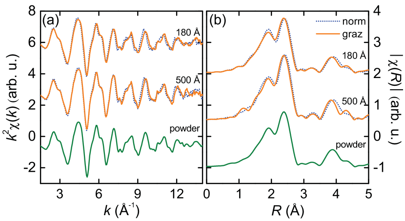
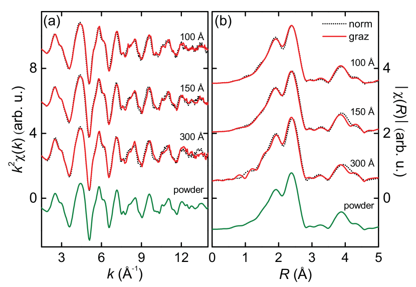
Figures 5 and 6 show the raw EXAFS signal and module of the Fourier transform (FT) of the thin films at normal and grazing geometries performed over a 3-13 Å-1 -range using a Hanning window function, and Å-1. All plots are performed using a weight. Data obtained for the powdered bulk MnSi is also included in these figures as reference. The shape and intensity of the spectra for thin films is, in general, similar to the one for bulk MnSi, with slight differences that might be related with the strain effects that we are looking for. The comparison between the normal and grazing incidence spectra for each sample shows subtle differences, which can be quantified by fitting the EXAFS signals.
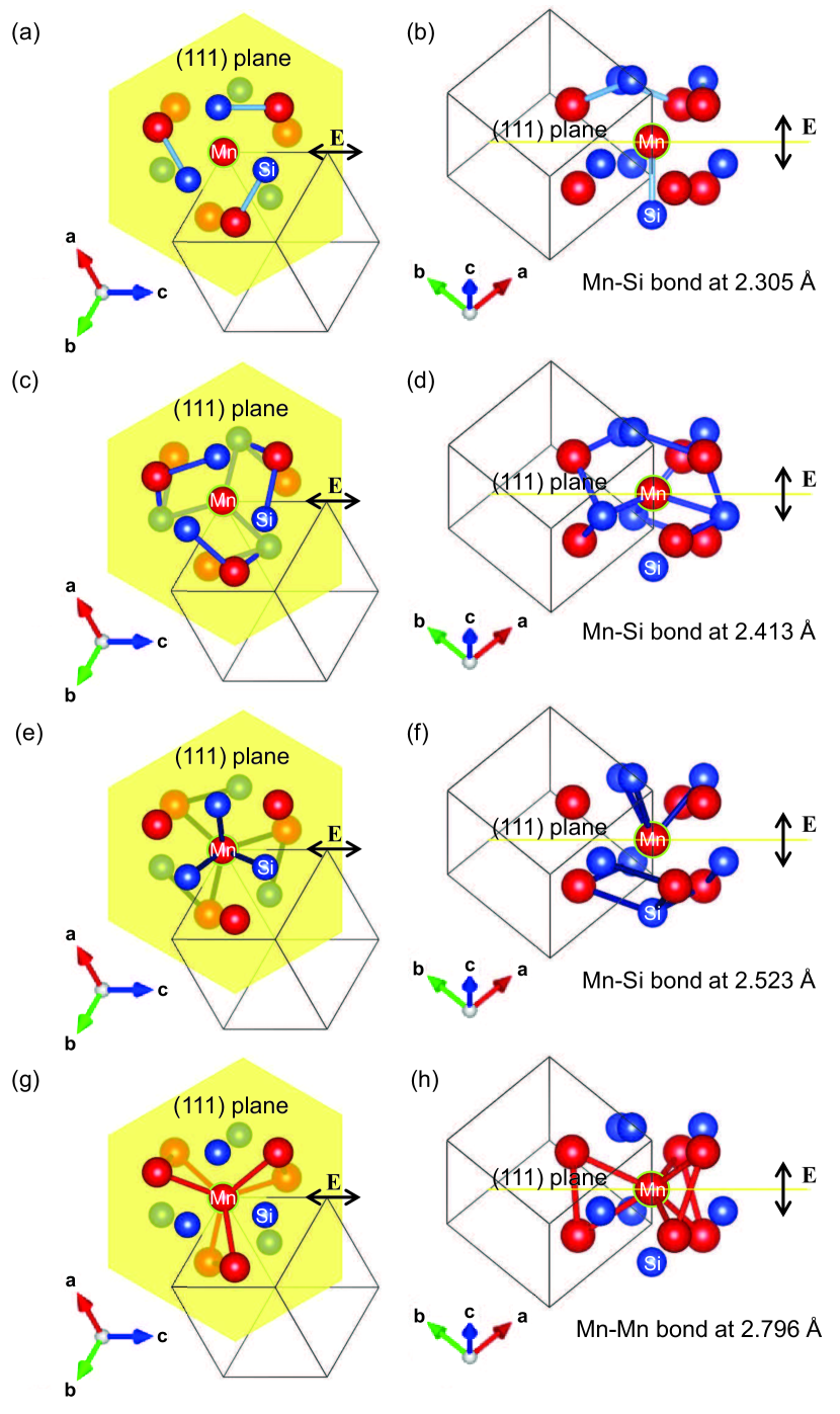
According to crystallographic information available for B20 MnSi in ICSD (71830),Jørgensen and Rasmussen (1991) the first coordination shell of Mn atoms in this structure is composed of seven Si neighbors (one at 2.305 Å, three at 2.413 Å, and three at 2.523 Å) and a second shell with six Mn neighbors at 2.796 Å. However, for the oriented thin films, given that the x-ray absorption is polarization-dependent, it is necessary to define an effective coordination numberBunker (2010) as
| (1) |
where is the angle between the electric-field vector E and the direction of the bond between the Mn atom and the neighbor of a given coordination shell with atoms. Note that Eq. (1) is only valid for polarization-dependent measurements at the edge.Bunker (2010) Taking the bonds from the first and second coordination shells for MnSi for each geometry (grazing and normal), as illustrated in Fig. 7, for each scattering path is calculated and listed in Table 1.
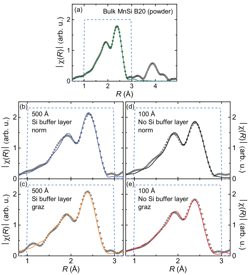
Fits of the Mn -edge EXAFS signal were performed in -space in a range of 1-3 Å using a Hanning window function, so that it covered the first two coordination shells of the Mn atoms (Fig. 8). The parameters fitted for the bulk MnSi (powder) sample were a general amplitude reduction factor () and shift in the threshold energy (), as well as the interatomic distance () and Debye-Waller factor () for each scattering path. The best fit of the EXAFS signal for bulk MnSi was obtained using a model which groups the first two Mn-Si bonds as four Mn-Si paths at 2.386 Å (Table 1). This approximation is needed due to limitations of the EXAFS technique in this particular case, as the results did not allow us to distinguish between the contribution of a single atom with respect to the one of three atoms at a very close distance. For the MnSi thin films, and were fixed to those values obtained for the bulk MnSi sample ( and eV) for both geometries. Results from these fits are listed in Table 1 and shown in Fig. 8. The Mn-Si-1, 2, and 3 bonds refer to the first, second, and third coordination shells, respectively.
| Geom | ||||||||||||||
| (Å) | (Å) | (Å2) | (Å) | (Å2) | (Å) | (Å2) | (Å) | (Å2) | ||||||
| Model111Bond distances extracted from ICSD 71830.Jørgensen and Rasmussen (1991) | - | aver | 1 | 2.305 | - | 3 | 2.413 | - | 3 | 2.523 | - | 6 | 2.796 | - |
| Model222Effective coordination numbers calculated using Eq. (1) and bonds obtained from ICSD 71830.Jørgensen and Rasmussen (1991) | - | norm | - | - | - | 4.12 | 2.413 | - | 1.86 | 2.523 | - | 6.98 | 2.796 | - |
| Model222Effective coordination numbers calculated using Eq. (1) and bonds obtained from ICSD 71830.Jørgensen and Rasmussen (1991) | - | graz | 3 | 2.305 | - | 0.76 | 2.413 | - | 5.27 | 2.523 | - | 4.04 | 2.796 | - |
| Bulk | - | - | - | - | - | 4 | 2.383 | 0.008 | 3 | 2.525 | 0.023 | 6 | 2.772 | 0.006 |
| Series | 500 | norm | - | - | - | 4.12 | 2.377 | 0.006 | 1.86 | 2.503 | 0.007 | 6.98 | 2.791 | 0.006 |
| 500 | graz | 3.76 | 2.405 | 0.016 | - | - | - | 5.27 | 2.441 | 0.014 | 4.04 | 2.774 | 0.003 | |
| 180 | norm | - | - | - | 4.12 | 2.380 | 0.005 | 1.86 | 2.536 | 0.006 | 6.98 | 2.801 | 0.008 | |
| 180 | graz | 3.76 | 2.388 | 0.010 | - | - | - | 5.27 | 2.467 | 0.020 | 4.04 | 2.773 | 0.004 | |
| Series | 300 | norm | - | - | - | 4.12 | 2.372 | 0.005 | 1.86 | 2.502 | 0.007 | 6.98 | 2.789 | 0.007 |
| 300 | graz | 3.76 | 2.440 | 0.027 | - | - | - | 5.27 | 2.418 | 0.010 | 4.04 | 2.773 | 0.003 | |
| 150 | norm | - | - | - | 4.12 | 2.383 | 0.005 | 1.86 | 2.536 | 0.005 | 6.98 | 2.792 | 0.007 | |
| 150 | graz | 3.76 | 2.411 | 0.010 | - | - | - | 5.27 | 2.445 | 0.021 | 4.04 | 2.772 | 0.003 | |
| 100 | norm | - | - | - | 4.12 | 2.382 | 0.004 | 1.86 | 2.549 | 0.005 | 6.98 | 2.789 | 0.008 | |
| 100 | graz | 3.76 | 2.413 | 0.008 | - | - | - | 5.27 | 2.443 | 0.023 | 4.04 | 2.773 | 0.003 |
From Table 1 and Fig. 7 we can conclude that there are bonds that contribute more to the EXAFS signal in one particular geometry. In fact, the Mn-Si-1 bond only contributes to the signal in grazing geometry, whereas Mn-Si-2 contributes mostly to that in normal incidence. The amplitude of the latter in grazing geometry is so low that it has no effect on the fit. Results of the bond length obtained for these two bonds are plotted for all thin films in Figs. 9(a) and 9(b), respectively. The values obtained for bulk (powder) MnSi for each bond and those from the crystallographic model (ICSD 71830Jørgensen and Rasmussen (1991)) are marked as reference on each plot.
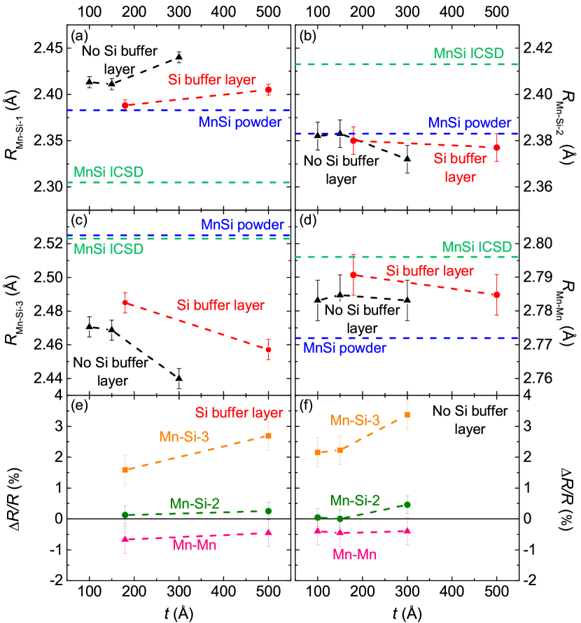
and its Debye-Waller factor increase with thickness for both sample series. This bond is longer for samples without Si buffer (series ) than those with buffer. For the 300-Å-thick sample, this bond length is at its maximum and the Debye-Waller factor is rather large, which suggests a large degree of disorder and/or distortion of this out-of-plane bond. Values for vary less within and between the sample series and are found to be very close to the value obtained for bulk MnSi. This result may indicate less in-plane distortion and/or strain in the thin films.
For Mn-Si-3 and Mn-Mn bonds, given that they contribute to both grazing and normal geometry, we have calculated a weighted average from the values obtained from the EXAFS fits. Resulting bond lengths are plotted in Figs. 9(c) and 9(d), respectively. for both sample series increases for decreasing thickness. There seems to be a slight increase in for both sample series, but it is within the error bar.
In order to analyze these results, we define the parameter
| (2) |
where is the bond length obtained from EXAFS fits for a given bond on a thin film sample and that obtained for the same bond for bulk (powder) MnSi. , expressed in %, provides quantitative information about the change in bond length of the films compared to that of the bulk (powder) sample, and it is proportional to the strain in the system. Results of obtained for each bond are plotted in Figs. 9(e) and 9(f) for the samples with and without Si buffer layer, respectively.
For films with Si buffer layer, for each bond does not vary significantly with film thickness [cf. Fig. 9(e)], whereas for samples of series without a buffer, the value increases with increasing film thickness [cf. Fig. 9(f)]. for Mn-Si-2 bonds on both sample series is negligible, which suggests low in-plane strain. Larger values of are found for Mn-Si-3 bonds, which, according to the model used for the analysis of the polarization dependence, is related to out-of-plane strain. It reaches 3.5% in samples without Si buffer, and 2.7% in those with a Si buffer.
These out-of-plane strain values, when taken as unit cell strain in an epitaxial film, are very large, whereas the in-plane strain is negligible. Interestingly, in this picture, the out-of-plane lattice constants of the films appear smaller than that of the bulk, meaning that the films should be compressively strained. This behavior is in contrast to previous reports in which tensile strain was found both in-planeWilson et al. (2014) and out-of-plane, using XRD and TEM, leading to an increase of the unit cell volume.Karhu et al. (2010) In Ref. Karhu et al., 2010, it was further shown that the critical temperature of the films is a linear function of the film thickness up to 10 nm, above which the saturates at 42 K (for films up to 22 nm thick). For compressively strained MnSi, e.g., in hydrostatic pressure studies of bulk crystals, a decrease of with increasing pressure was reported.Pfleiderer et al. (2004) In fact, above 14.6 kbar long-range magnetic order is fully suppressed.Pfleiderer et al. (2004) Recent hydrostatic pressure studies on MnSi thin films on Si(111) have shown that this critical pressure is enhanced to 31 kbar.Engelke et al. (2014)
Using the elastic constants of MnSi of dyn/cm2, dyn/cm2, and dyn/cm2 (all at 6.5 K),Petrova et al. (2011) we obtain a bulk modulus for this cubic system of dyn/cm2 = 164 GPa and a shear modulus of = 126 GPa. Young’s modulus can then be calculated from GPa.Lay and Wallace (1995) With the tensile stress , where is the strain, we obtain 1.46 GPa/(301 GPa) (3.1 GPa/(301 GPa) ), i.e., above a strain value of 0.5% (1.0%) magnetic long-range order, and thus the skyrmion state, are suppressed in bulk crystals (films).
Interestingly, for the films studied here, a of 46.6 K (series ) and 44 K (series ), respectively, was observed, roughly consistent with the previously reported values for thick, epitaxial MnSi films (10 nm).Karhu et al. (2010) As these values for the transition temperature are in fact equal or even slightly higher than the values for the tensile strained films, strain does not seem to have a straightforward and direct effect on magnetic ordering in MnSi films (in the thick film limit). In order to shed more light on the apparent discrepancy, we performed a structure refinement of the crystal structure based on the EXAFS results.
IV.2 Lattice structure analysis
One of the main conclusions that can be drawn from the polarization-dependent EXAFS analysis is that the bond distances in thick, epitaxial MnSi films predominantly undergo out-of-plane changes. This finding enables us to perform a structure refinement starting from the measured bond distances.
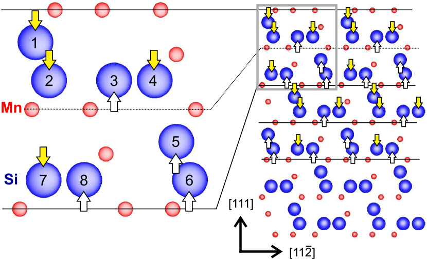
For the structural refinement, first, the EXAFS data obtained from a (bulk) MnSi powder sample was analyzed, and a good agreement with the published ICSD dataJørgensen and Rasmussen (1991) was found. Then, the crystalline model for bulk MnSi was used as the reference. MnSi crystallizes in the simple cubic B20 structure with four Mn and four Si atoms in the unit cell (space group ). The Wyckoff positions are (, , ), (+, , +), (, +, +, (+, +, ), with and .van der Marel et al. (1998) The Mn atom has a seven-fold coordination of Si atoms.van der Marel et al. (1998) It is worth stressing again that EXAFS is only sensitive to the bond distances between atoms (not the atomic positions themselves). In our EXAFS measurements, the length of seven Si-Mn bonds and six Mn-Mn bonds were extracted. We can unambiguously associate these 14 atomic positions with the space group symmetries. In other words, by setting the position of an arbitrary Mn atom as a reference, the positions of the measured 14 atoms can be determined for the MnSi bulk model. Next, it is assumed that these atoms only move along the [111] direction, which is justified from the polarization-dependent EXAFS analysis in Sec. IV.1.
As each of these atoms shows a varied bond distance in thin films, their specific atomic positions can be determined by carrying out a data fitting procedure, giving the deviations from the Wyckoff positions summarized in Table 2. Note that the seven positions around the Mn are now all different. The deviations from the bulk Wyckoff positions are termed , with Sii (). We formally included an eighth Si atom for illustration purposes (cf. Fig. 10), which corresponds to a doubling of the unit cell in which one Si double-layer moves predominantly down, and the adjacent double-layer layer up, indicated by yellow and white arrows, respectively. Interestingly, the Mn positions have not changed beyond the uncertainty in determining the shift of their position along [111] of Å.
The absence of a shift of the Mn atoms means that the unit cell volume remains constant for epitaxial MnSi films in the thick film limit and we can therefore exclude (volume) strain in these films as the source for both the enhanced and the absence of the skyrmion phase. Further, as the Mn atoms do not move, the direct interactions between the Mn atoms are unaltered, suggesting that the balance between the exchange and the Dzyaloshinskii-Moriya interactions remains unchanged. This view is further supported by magnetometry data that show a similar behavior of MnSi thin films and bulk material.Zhang et al. (2016) In a simple Heisenberg picture one would expect an increase in only for a decreasing Mn-Mn bond distance, which we can clearly rule out.Geisler and Kratzer (2013) However, as the Si atoms move in films with an increased , another coupling mechanism, involving Si, may be present as well. For example, the change of the positions of the Si atoms could change the crystal field affecting the magnetic ions.
| Series | ||||||||
| (Å) | (Å) | (Å) | (Å) | (Å) | (Å) | (Å) | (Å) | |
| 500 | ||||||||
| 180 | 0.1279 | 0.0708 | 0.0299 | 0.0247 | ||||
| 300 | 0.1969 | 0.1732 | 0.0660 | 0.0307 | ||||
| 150 | 0.1592 | 0.1048 | 0.0429 | 0.0224 | ||||
| 100 | 0.1619 | 0.1007 | 0.0414 | 0.0232 |
V Conclusions
In conclusion, we have performed polarization-dependent EXAFS measurements on MnSi thin films grown on Si(111) as a function of film thickness in order to explore strain in the samples. The investigated films are in the thick film limit, i.e., between 100 and 500 Å, where the magnetic properties are no longer a strong function of film thickness. Despite the high quality of the phase-pure B20 MnSi films, and the presence of a sharp interface between MnSi and Si, no unambiguous detection of skyrmions in these films has been reported. As confirmed by EXAFS analysis, the in-plane strain is negligible. The out-of-plane strain, as defined by the relative contraction of the bonds along [111], is negative and as high as 3.5% for samples without a Si buffer layer and 2.7% for buffered systems. Nevertheless, the refinement of the atomic positions reveals that the change in bond lengths has different effects on Mn and Si. Whereas the positions of the Mn atoms in the crystal lattice remain unchanged, the Si atoms move along the out-of-plane [111]-direction, predominantly in opposite directions in neighboring unit cells. The unit cell of thick MnSi films is therefore effectively unstrained. Nevertheless, the magnetic transition temperature in the thick film limit is enhanced by 15 K as compared to the bulk, and no longer a function of film thickness, suggesting a far-reaching effect of the interface with the substrate. Another factor could be surface effects, which are effective down to a finite depth and which therefore saturate as the film is thicker than a critical thickness. Finally, the shifted Si positions could have an indirect effect on the magnetic ordering of the Mn atoms, e.g., via the crystal field. Therefore, more work is needed that focuses on the study of interfacial strain, surface effects, and the generation of chemical pressure through doping, to be able to stabilize the skyrmion phase in B20 thin films, while simultaneously increasing the magnetic transition temperature.
Finally, we would like to stress that the analysis of polarization-dependent EXAFS performed here to investigate the local strain at the MnSi/Si(111) interface can be widely employed, e.g., to study superconducting latticesFogel et al. (2001); Tang and Fu (2014) or heterostructures incorporating topological insulators.Vobornik et al. (2011); Li et al. (2015) This methodology provides invaluable information about the local interfacial structure, and may allow to explore its correlation with their fascinating electronic and magnetic properties.
Acknowledgements.
We acknowledge Diamond Light Source for beamtime on B18 under proposal SP-10243, and financial support by the John Fell Oxford University Press (OUP) Research Fund. TH and SLZ acknowledge support by the Semiconductor Research Corporation (SRC), and AAB partial financial support by Diamond, EPSRC and Wadham College, Oxford. RC acknowledges the Israel PBC fellowship for support. AK acknowledges the support of the Israel Science Foundation (grant 1321/13). CP acknowledges financial support through DFG TRR80 and ERC AdG (291079, TOPFIT). We thank N.-J. Steinke and L. B. Duffy for help with the XRD/XRR measurements, and R. Boada and P. Böni for fruitful discussions.References
- Mühlbauer et al. (2009) S. Mühlbauer, B. Binz, F. Jonietz, C. Pfleiderer, A. Rosch, A. Neubauer, R. Georgii, and P. Böni, Science 323, 915 (2009).
- Pfleiderer et al. (2010) C. Pfleiderer, T. Adams, A. Bauer, W. Biberacher, B. Binz, F. Birkelbach, P. Böni, C. Franz, R. Georgii, M. Janoschek, F. Jonietz, T. Keller, R. Ritz, S. Mühlbauer, W. Münzer, A. Neubauer, B. Pedersen, and A. Rosch, J. Phys.: Condens. Matter 22, 164207 (2010).
- Nagaosa and Tokura (2013a) N. Nagaosa and Y. Tokura, Nat. Nanotechnol. 8, 899 (2013a).
- Adams et al. (2011) T. Adams, S. Mühlbauer, C. Pfleiderer, F. Jonietz, A. Bauer, A. Neubauer, R. Georgii, P. Böni, U. Keiderling, K. Everschor, M. Garst, and A. Rosch, Phys. Rev. Lett. 107, 217206 (2011).
- Neubauer et al. (2009) A. Neubauer, C. Pfleiderer, B. Binz, A. Rosch, R. Ritz, P. G. Niklowitz, and P. Böni, Phys. Rev. Lett. 102, 186602 (2009).
- Jonietz et al. (2010) F. Jonietz, S. Mühlbauer, C. Pfleiderer, A. Neubauer, W. Münzer, A. Bauer, T. Adams, R. Georgii, P. Böni, R. A. Duine, K. Everschor, M. Garst, and A. Rosch, Science 330, 1648 (2010).
- Yu et al. (2010) X. Z. Yu, Y. Onose, N. Kanazawa, J. H. Park, J. H. Han, Y. Matsui, N. Nagaosa, and Y. Tokura, Nature 465, 901 (2010).
- Yu et al. (2011) X. Z. Yu, N. Kanazawa, Y. Onose, K. Kimoto, W. Z. Zhang, S. Ishiwata, Y. Matsui, and Y. Tokura, Nat. Mater. 10, 106 (2011).
- Tonomura et al. (2012) A. Tonomura, X. Yu, K. Yanagisawa, T. Matsuda, Y. Onose, N. Kanazawa, H. S. Park, and Y. Tokura, Nano Lett. 12, 1673 (2012).
- Heinze et al. (2011) S. Heinze, K. von Bergmann, M. Menzel, J. Brede, A. Kubetzka, R. Wiesendanger, G. Bihlmayer, and S. Blügel, Nat. Phys. 7, 713 (2011).
- Zhang et al. (2015) S. L. Zhang, A. A. Baker, S. Komineas, and T. Hesjedal, Sci. Rep. 5, 15773 (2015).
- Nagaosa and Tokura (2013b) N. Nagaosa and Y. Tokura, Nat. Nanotechnol. 8, 899 (2013b).
- Milde et al. (2013) P. Milde, D. Köhler, J. Seidel, L. M. Eng, A. Bauer, A. Chacon, J. Kindervater, S. Mühlbauer, C. Pfleiderer, S. Buhrandt, C. Schütte, and A. Rosch, Science 340, 1076 (2013).
- Schwarze et al. (2015) T. Schwarze, J. Waizner, M. Garst, A. Bauer, I. Stasinopoulos, H. Berger, C. Pfleiderer, and D. Grundler, Nat. Mater. 14, 478 (2015).
- Münzer et al. (2010) W. Münzer, A. Neubauer, T. Adams, S. Mühlbauer, C. Franz, F. Jonietz, R. Georgii, P. Böni, B. Pedersen, M. Schmidt, A. Rosch, and C. Pfleiderer, Phys. Rev. B 81, 041203 (2010).
- Karhu et al. (2010) E. Karhu, S. Kahwaji, T. L. Monchesky, C. Parsons, M. D. Robertson, and C. Maunders, Phys. Rev. B 82, 184417 (2010).
- Karhu et al. (2011) E. A. Karhu, S. Kahwaji, M. D. Robertson, H. Fritzsche, B. J. Kirby, C. F. Majkrzak, and T. L. Monchesky, Phys. Rev. B 84, 060404 (2011).
- Karhu et al. (2012) E. A. Karhu, U. K. Rößler, A. N. Bogdanov, S. Kahwaji, B. J. Kirby, H. Fritzsche, M. D. Robertson, C. F. Majkrzak, and T. L. Monchesky, Phys. Rev. B 85, 094429 (2012).
- Wilson et al. (2012) M. N. Wilson, E. A. Karhu, A. S. Quigley, U. K. Rößler, A. B. Butenko, A. N. Bogdanov, M. D. Robertson, and T. L. Monchesky, Phys. Rev. B 86, 144420 (2012).
- Wilson et al. (2013) M. N. Wilson, E. A. Karhu, D. P. Lake, A. S. Quigley, S. Meynell, A. N. Bogdanov, H. Fritzsche, U. K. Rößler, and T. L. Monchesky, Phys. Rev. B 88, 214420 (2013).
- Li et al. (2013) Y. Li, N. Kanazawa, X. Z. Yu, A. Tsukazaki, M. Kawasaki, M. Ichikawa, X. F. Jin, F. Kagawa, and Y. Tokura, Phys. Rev. Lett. 110, 117202 (2013).
- Menzel et al. (2013) D. Menzel, J. Engelke, T. Reimann, and S. Süllow, J. Korean Phys. Soc. 62, 1580 (2013).
- Wilson et al. (2014) M. N. Wilson, A. B. Butenko, A. N. Bogdanov, and T. L. Monchesky, Phys. Rev. B 89, 094411 (2014).
- Yokouchi et al. (2015) T. Yokouchi, N. Kanazawa, A. Tsukazaki, Y. Kozuka, A. Kikkawa, Y. Taguchi, M. Kawasaki, M. Ichikawa, F. Kagawa, and Y. Tokura, J. Phys. Soc. Jpn. 84, 104708 (2015).
- Zhang et al. (2016) S. L. Zhang, R. Chalasani, A. A. Baker, N.-J. Steinke, A. I. Figueroa, A. Kohn, G. van der Laan, and T. Hesjedal, AIP Adv. 6, 015217 (2016).
- Meynell et al. (2014) S. A. Meynell, M. N. Wilson, J. C. Loudon, A. Spitzig, F. N. Rybakov, M. B. Johnson, and T. L. Monchesky, Phys. Rev. B 90, 224419 (2014).
- Müller et al. (2016) J. Müller, A. Rosch, and M. Garst, (2016), arXiv:, 1601.06922 .
- Engelke et al. (2014) J. Engelke, D. Menzel, H. Hidaka, T. Seguchi, and H. Amitsuka, Phys. Rev. B 89, 144413 (2014).
- Chacon et al. (2015) A. Chacon, A. Bauer, T. Adams, F. Rucker, G. Brandl, R. Georgii, M. Garst, and C. Pfleiderer, Phys. Rev. Lett. 115, 267202 (2015).
- Nii et al. (2015) Y. Nii, T. Nakajima, A. Kikkawa, Y. Yamasaki, K. Ohishi, J. Suzuki, Y. Taguchi, T. Arima, Y. Tokura, and Y. Iwasa, Nat Commun. 6, 8539 (2015).
- Kahwaji et al. (2012) S. Kahwaji, R. A. Gordon, E. D. Crozier, and T. L. Monchesky, Phys. Rev. B 85, 014405 (2012).
- Fogel et al. (2001) N. Y. Fogel, A. S. Pokhila, Y. V. Bomze, A. Y. Sipatov, A. I. Fedorenko, and R. I. Shekhter, Phys. Rev. Lett. 86, 512 (2001).
- Tang and Fu (2014) E. Tang and L. Fu, Nat. Phys. 10, 964 (2014).
- Vobornik et al. (2011) I. Vobornik, U. Manju, J. Fujii, F. Borgatti, P. Torelli, D. Krizmancic, Y. S. Hor, R. J. Cava, and G. Panaccione, Nano Letters 11, 4079 (2011).
- Li et al. (2015) M. Li, C.-Z. Chang, B. J. Kirby, M. E. Jamer, W. Cui, L. Wu, P. Wei, Y. Zhu, D. Heiman, J. Li, and J. S. Moodera, Phys. Rev. Lett. 115, 087201 (2015).
- Engelke et al. (2012) J. Engelke, T. Reimann, L. Hoffmann, S. Gass, D. Menzel, and S. Süllow, J. Phys. Soc. Jpn. 81, 124709 (2012).
- Geisler and Kratzer (2013) B. Geisler and P. Kratzer, Phys. Rev. B 88, 115433 (2013).
- Geisler et al. (2012) B. Geisler, P. Kratzer, T. Suzuki, T. Lutz, G. Costantini, and K. Kern, Phys. Rev. B 86, 115428 (2012).
- Kumar et al. (2004) A. Kumar, M. Tallarida, M. Hausmann, U. Starke, and K. Horn, J. Phys. D - Appl. Phys. 37, 1083 (2004).
- Ravel and Newville (2005) B. Ravel and M. Newville, J. Synchrotron Rad. 12, 537 (2005).
- Ravel (2001) B. Ravel, J. Synchrotron Rad. 8, 314 (2001).
- Jørgensen and Rasmussen (1991) J.-E. Jørgensen and S. E. Rasmussen, Powder Diffr. 6, 194 (1991).
- Bunker (2010) G. Bunker, Introduction to XAFS. A Practical Guide to X-ray Absorption Fine Structure Spectroscopy (Cambridge University Press, 2010).
- Pfleiderer et al. (2004) C. Pfleiderer, D. Reznik, L. Pintschovius, H. v. Löhneysen, M. Garst, and A. Rosch, Nature 427, 227 (2004).
- Petrova et al. (2011) A. E. Petrova, V. N. Krasnorussky, W. M. Yuhasz, T. A. Lograsso, and S. M.Stishov, J. Phys.: Conf. Ser. 273, 012056 (2011).
- Lay and Wallace (1995) T. Lay and T. C. Wallace, Modern Global Seismology (Academic Press, San Diego, 1995).
- van der Marel et al. (1998) D. van der Marel, A. Damascelli, K. Schulte, and A. Menovsky, Physica B 244, 138 (1998).