Trembling electrons cause conductance fluctuation
Abstract
The highly successful Dirac equation can predict peculiar effects such as Klein tunneling and the “Zitterbewegung” (German for “trembling motion”) of electrons. From the time it was first identified by Erwin Schrödinger, Zitterbewegung (ZB) has been considered a key to understanding relativistic quantum mechanics. However, observing the original ZB of electrons is too difficult, and instead various emulations using entity models have been proposed, producing several successes. Expectations are high regarding charge transports in semiconductors and graphene; however, very few reports have appeared on them. Here, we report that ZB has a surprisingly large effect on charge transports when we play “flat pinball” with such trembling electrons in a semiconductor nanostructure. The stage here is a narrow strip of InAs two-dimensional electron gas with a strong Rashba spin-orbit coupling. Six quantum point contacts (QPCs) are attached to the strip as pinball pockets. The ZB appeared as a large reproducible conductance fluctuation versus in-plane magnetic fields in the transport between two QPCs. Numerical simulations successfully reproduced our experimental observations, certifying that ZB causes a new type of conductance fluctuation.
In 1930, Erwin Schrödinger [1] found that a free particle described by the relativistic Dirac equation undergoes oscillatory motion with the light velocity . This phenomenon, called Zitterbewegung (meaning “trembling motion” and abbreviated as ZB), originates from the pure quantum nature of relativistic velocity, which does not commute, as an operator, with the Dirac Hamiltonian. This means the velocity, despite long being a most familiar quantity to physicists, is not a good quantum number for a free relativistic particle. Although interest in this remarkable nature was stimulated among researchers, its estimated amplitude 386 fm, and the frequency rad./s for electrons, keep it very far out of experimental reach[2]. Successful ZB emulations have been achieved in entity models, including those with a single trapped ion[3] and ultra-cold atoms in Bose-Einstein condensates[4, 5]. However, clear observation of ZB in more realistic emulations with electrons themselves in artificial vacuums, namely in solids[6, 7, 8], has been a major open task. In two-dimensional electron systems with Rashba-type spin-orbit coupling (SOC)[9], ZB is predicted to appear as a meandering of charge density[6] with relatively large amplitude of more than ten nanometers [8], which is still barely observable by utilizing nanoscale techniques and superfine structures (although a possible observation was reported in a mesoscopic device[10]).
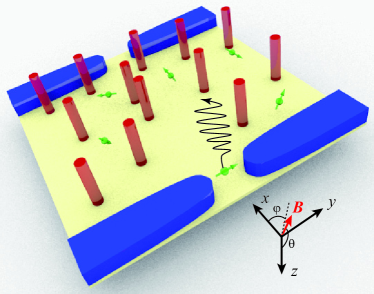
Here, we report observation of ZB as reproducible conductance fluctuation (CF) versus magnetic fields in an InAs two-dimensional electron gas (2DEG) fabricated into an open billiard geometry, which has quantum point contacts (QPCs) as emitters and billiard pockets. However, the experiment can be viewed as a pinball on a flat table (see Fig.1) rather than as a billiard, because the table has a considerable number of fixed scatterers (impurities). The “flat pinball with trembling electrons” model is also verified using a numerical simulation, which exhibits meandering of charge density and reproduces CF.
Results
ZB in Rashba model
Let us briefly view how ZB appears in the Rashba model described by the Hamiltonian
| (1) |
where is the electron momentum, the effective mass, the Rashba SOC parameter, the effective Landé g-factor, the Bohr magneton, (with , as the unit coordinate vectors) the in-plane magnetic flux density, and the Pauli matrices. As an initial condition (), we consider an electron with a spin state of -up in a Gaussian wavepacket at an origin with central wave vector (vector along with size ). After a time evolution of , the expectation value of the -coordinate for finite is[11],
| (2) |
where
| (3) |
while the spin portion of the wavefunction is written as . In the limit , the amplitude of the ZB in Eq.(2) vanishes while it approaches for .
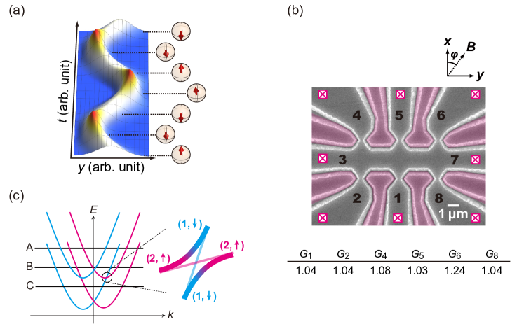
Figure 2 (a) shows a schematic trace of the wavepacket oscillating along according to Eq.(2) with spin directions. As is easily understood, in a Rashba system, ZB appears as a meandering electron orbit with a spin precession around the vector sum of and an effective magnetic field originating from SOC
| (4) |
which is perpendicular to the momentum.
In the above formulas, the difficulties in the detection are apparent in that 1) the ZB amplitude is the Fermi wavelength at most, and 2) to attain this amplitude the ZB frequency in Eq.(3) should be very high — above 1 THz. In the following, we consider solving these problems in the introduction of the experimental setup.
Experimental setup
To create a Rashba system, a 2DEG in a pseudomorphic InAs quantum well was grown with molecular beam epitaxy. The layered structure has asymmetric (In,Ga)As/InAs interfaces in the well region, whose structure is commonly adopted for strong Rashba SOI[12]. The electron mobility = 6.6 cm2/Vs and the sheet carrier concentration were obtained from the longitudinal and Hall resistances. They produced the Fermi wavenumber = 2.6 m-1, which corresponds to wavelength 2.4 m. The effects of quantum confinement, wavefunction penetration into (In,Ga)As, and strain is renormalized into a shift in the in-plane effective mass in InAs from bulk value 0.023 to 0.025[13]. Then, the Fermi velocity m/s and the Fermi energy meV, 8.6[14] were obtained. The Rashba parameter was obtained from the amplitude modulation of the Shubnikov-de Haas (SdH) conductance oscillation[15]. These parameters give the effective magnetic field strength (4) as 38 T, hence the ZB frequency 4.6 THz.
The high frequency problem can be solved by fixing the ZB in a steady state by using spin-polarized electrons. This can be accomplished with a quantum point contact (QPC) on the conductance plateau of quantum conductance , which was predicted theoretically[16] and confirmed experimentally[17]. Figure 2 (c) illustrates how the mechanism works to polarize spins of electrons passing through a QPC with Rashba SOI on the conductance plateau of . On the top of the effective potential in the QPC, the Fermi energy places at the lowest branch in the discrete dispersion relations. When an electron passes through the QPC adiabatically, its energy shifts as A B C B’ A’. During the transition from C to B’, the avoided crossing between (0) and (1) flips up the electron spin. Owing to the “one-way spin rotation,” the spin polarization on plateau reaches 0.7. Here, the spin separation of the dispersion branch comes from the term, and the avoided crossing comes from in (1). The Rashba SOI is thus necessary for the spin polarization.
Figure 2(b) shows a scanning electron micrograph from the sample, on which the numbers of the terminals are indicated. A right-handed spatial coordinate with a -axis perpendicular to the 2DEG plane is taken as illustrated. The structure was fabricated with electron beam lithography and dry etching of trenches. Such trench-gate techniques are commonly used in InAs-based heterostructures[18], to which the Schottky gate technique is hardly applicable. The structure consists of a main conducting strip (terminal 3-7) with a width of 2 m and six QPCs opened on it. A problem here is that the gates (pink false-colored regions) are common with the neighboring ones and individual control of QPC conductance is difficult. Fortunately, after several cut-and-tries, we succeeded in tuning the QPC conductances at around 1.0 with all the gates grounded (except QPC-6), as shown in Fig.2(b). The fact that such coarse tuning was successful indicates that the QPCs are on the 1.0 plateau, where the conductance is less sensitive to the gate voltages than in other regions.
Then, in a conduction through any two of the QPCs, we emit spin-polarized electrons into the main strip region in one QPC and collect them through the other one. Owing to the electron-hole symmetry, this holds even for conduction paths with QPC-6, in which the polarization may be insufficient. However, the effective opening of the QPCs is around 500 nm, which is still much wider than the maximum amplitude of ZB. Here, we attempt to solve the problem by using the scatterers in the strip as amplifiers of the meandering motions. Because the width of the present mean free path 1 m is about half that of the main strip, the emitted electrons should experience a few scatterings before reaching a pocket. If we approximate such a scattering with a classical scattering for a hard cylindrical wall with radius , the scattering angle for impact factor is . When oscillates against in-plane magnetic field through a ZB with amplitude , the oscillation is amplified to . The potential range is roughly estimated to be an effective Bohr radius of 34 nm in InAs, which is even smaller than . Hence, the amplified ZB can reach the order of m, which can be resolved with the present QPCs.
The above rough classical sketch of scattering should be largely corrected in quantum mechanics, in that the spread of wave packets weakens the amplification. As in the spin-polarization mechanism illustrated in Fig.2 (c), the wave packets emitted from a QPC should cover at least . However, as shown experimentally in scanning gate microscopy[19], the wave packets emitted from a QPC travel for surprisingly long distances without smooth spreading, owing to a kind of focusing effect. Therefore, we can expect that the above classical model can be half-quantitatively applicable. The experimental setup here can be viewed as a game of pinball on a flat table with six pockets. The ball (wave packet) size may be larger than the pins (scattering centers), although minor wobbling in the orbits (the ZB) is amplified by the scattering.
Conductance fluctuations
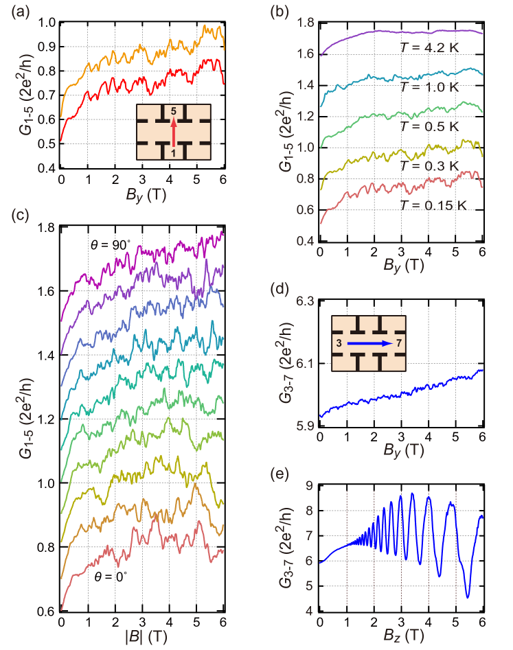
Henceforth, we use the notation for the two-wire conductance between terminals and . Figure 3 (b) shows temperature variation of the two-wire conductance as a function of the in-plane magnetic field along -axis . When the temperature was decreased, some aperiodic conductance oscillation versus became visible and the amplitude increased. The oscillation is reproducible, that is, almost the same pattern appears for two independent field sweeps at the same temperature, as demonstrated in Fig. 3 (a). Resemblances are also appreciable between the patterns for different temperatures. Such conductance fluctuations (CFs), that is, the aperiodic response to an external magnetic field, were observed for an arbitrary combination of two electrodes for QPC connections.
The result indicates that ZB is modulated by an external magnetic field and appears as CFs in the pinball model. However, these remarkable features of CFs are also reminiscent of so-called universal conductance fluctuation (UCF)[20]. We should thus check for the possibility of UCF. Because the applied field is in-plane, we can eliminate the quantum interference effect through random paths tuned via the Aharonov-Bohm (AB) phase. However, there still remains the possibility of interference in the spin portion of the wavefunction, which is modified by a spin precession tuned via the in-plane magnetic field (spin-UCF) [21]; for the elimination, we need the following two experiments.
The first is the rotation of the field direction from in-plane to perpendicular-to-plane (i.e., rotating the elevation angle from 0 to /2). The result is shown in Fig.3 (c). There is no significant variation in the amplitude and frequency distribution resulting from the pattern changes involving the angle. This is hardly conceivable for interference type CF, because if there is such a network of spatial interference and the perpendicular component of the field is increased, the AB phase modulation participates in the interference modulation, which should bring some qualitative and systematic changes in the CF that stem from the geometric nature of the AB phase. The second is the magnetic response of , i.e., a transport without QPCs (and hence without spin polarization). Figures 3 (d, e) display the result, which exhibits a dramatic change from Fig. 3 (c), in that in almost no fluctuation is observable in the in-plane field and ordinary SdH oscillation appearing in the perpendicular field (although the SOI modulation is reduced, probably by loose confinement into the strip). This also indicates that the CFs are not from an interference because if such an interference exists, it inevitably appears in , the path of which goes through the strip.
The most plausible origin of the CFs is now the ZB modulation of scattering in the pinball system; thus, we further check the nature of CFs. The pinball model has two temperature factors; one is the spin polarization at QPCs and the other is the strength of the effective field . The latter is related to Rashba splitting, which is approximately 6 K in the present case. The CF is visible at order-of-magnitude lower temperatures. Hence, the temperature dependence observed in Fig.3 (b) should come from spin polarization, which depends on the energy diagram inside the QPCs. Derivation of the explicit temperature dependence is difficult, although the order estimation is reasonable because the effective is lower by an order of magnitude inside the QPCs.
Azimuth angle dependence
Figure 4 (a) shows the variation of CF on the azimuth angle for an in-plane magnetic field. The fluctuation pattern changes with according to its resemblance to neighboring patterns. A frequency amplitude spectra obtained with a fast Fourier transform (FFT) is shown in Fig.4 (b); it indicates some systematic angular dependence in the width of spectra.
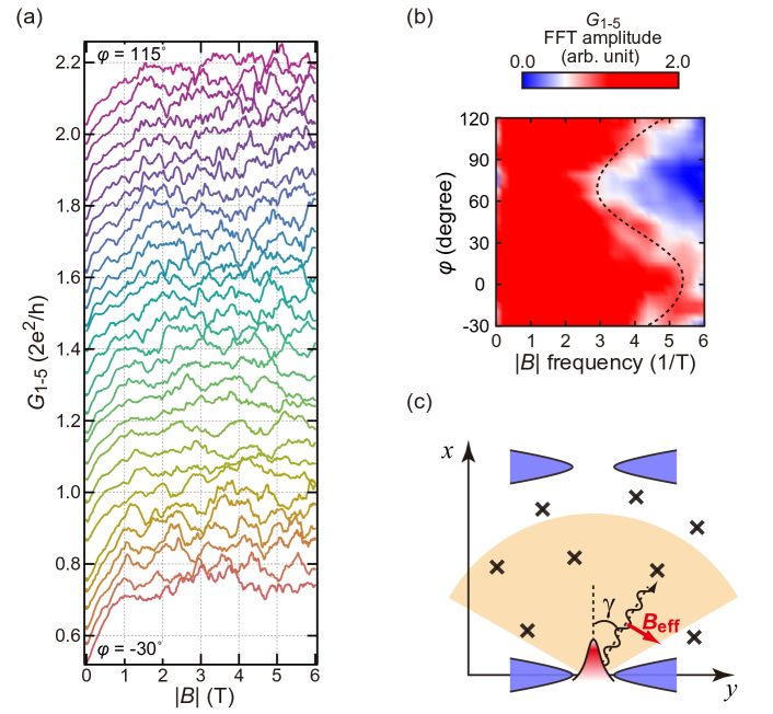
Let us check the correspondence between the pinball game model and the experimental results. Because the spin polarization is along the -axis directly near the emitter QPC[16], the electrons with momentum parallel to the -axis do not tremble because is perpendicular to the momentum from Eq.(1), which is parallel to the spins. Now we consider a path with an oblique angle to the -axis (Fig.4(c)). The length of is approximated as , where is the external field strength and for . The “wavelength” of ZB is estimated as 270nm and the maximum modification of with an external field for =6 T and is 34 nm. This means only a single cycle of meander changes in the traversal of 2 m for 6 T.
However, this does not mean maximum frequency 1/6 T-1 is expected in the CL. Because a channel opening of a scattered orbit is for a very narrow range of magnetic fields, the conductance for the opening appears as a narrow peak, which contains high-frequencies magnetic responses. As illustrated in Fig.4(c), if there are scatterers inside a “fan” of initial momentums, there should appear to such conductance peaks corresponding to channels with a single scattering within 6 T, forming a fluctuation pattern. The density and sharpness of conductance peaks increases for channels with more scatterings, while the peak height decreases. In the FFT power spectra, such gradual tailing to high frequencies is actually observed. In the conduction from terminal 5 to 1, the paths should distribute around . Thus, we further approximate . Further, the -dependence of the power spectral width is roughly written as
| (5) |
where is the averaged ZB path length. Although the approximation is very coarse, Eq.(5) suggests that takes a maximum around 90∘ and a minimum around 0∘, which is clearly recognizable in Fig.4 (b).
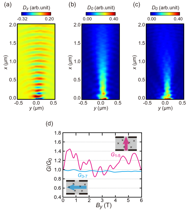
An interesting test is to change the combination of electrodes. Figure 5 (a) shows results of the same experiment as Fig.4 (b) but for the conductance between electrodes 5 and 2. Now, the center of path distribution is around , and -dependence in Eq.(5)should change to as is indeed observed in Fig.5 (a). Figure 5 (c) shows the CLs for three different combinations of electrodes under an external magnetic field with . The difference between and can be explained by a shift in -dependence. More interesting is , in which backscatterings are inevitable; hence, paths with multiple scatterings survive, resulting in reduced amplitude fluctuation and higher frequencies. In , the QPC path selection mechanism QPC does not work, although coupling with transverse modes should be required. The ZB-induced oscillation in the coupling causes residual conductance fluctuation with much smaller amplitude.
Tight binding calculation
Thus far, we have checked the ZB in a simple pinball model from various viewpoints. Here, we show that ZB and impurity scattering causes significant fluctuation in the conductance between QPCs in the Rashba model with numerical calculations.
Figure 6(a-c) shows the spatial distribution of spin-polarized electrons in a steady flow from a narrow constriction into a clean two-dimensional region. Clear meandering is observed, confirming the existence of ZB. Figure 6(d) displays conductance by electrons with and without spin-polarization between two constrictions through a strip region with scatterers. The conductance shows a large aperiodic response to an in-plane magnetic field for spin-polarized electrons, while such fluctuation is much smaller for unpolarized electrons. Note that we take an absorptive boundary condition, which breaks the unitarity. This is to kill unrealistic conductance fluctuation due to interference with infinite coherence. The residual conductance fluctuation for spin-unpolarized electrons should come from such interference on paths without bounce to the boundaries. The result indicates that, in a Rashba system with scatterers, ZB truly causes conductance fluctuation, supporting some reality of the pinball model.
Methods
Two-dimensional electron system in an InAs quantum well
The substrate was an InAs quantum well, grown on a (001) InP using the molecular beam epitaxy technique. It consists of, from the bottom, InAlAs and InGaAs (700 nm) as buffer layers, InAs (4 nm), InGaAs (4 nm), InAlAs (10 nm), n-InAlAs (40 nm), InAlAs (5 nm), and InGaAs (2 nm). QPCs were fabricated by electron-beam lithography and Ar dry-etching with the depth of 300 nm. Contacts were fabricated by AuGe deposition (100 nm) and subsequent annealing (280 degree, 5 min).
The specimen was cooled to 70 mK in a dilution fridge with a superconducting solenoid for applying the magnetic field. A conventional lock-in technique was used for measuring two-wire conductances with frequencies lower than 1 kHz.
Setups for numerical calculations
For numerical calculations we employed the “Kwant” package[22], which is based on a tight-binding approximation. The distance between two QPCs , QPC width , and Rashba strength were adopted to simulate the experiment. The effective mass (where is the electron mass in vacuum) and g-factor were adopted from previous studies [13]. was tuned to give the QPC conductance . The calculated area was , and was surrounded by absorption walls (except for the QPC passes) and simplified to a square lattice with the lattice constant . Impurities were introduced by adding randomly-distributed values to onsite energy. The typical amplitudes of the impurities were .
References
References
- [1] Schrödinger, E. Über die kraftefreie Bewegung in der relativistischen Quantenmechanik. Sitzungsber. Preuss. Akad. Wiss. Berl. Phys.-math. Kl. 24, 418-428 (1930).
- [2] Zawadzki, W. and Rusin, T. M. Zitterbewegung (trembling motion) of electrons in semiconductors: a review. J. Phys.: Condens. Matter 23, 143201 (2011).
- [3] Gerritsma, R. et al. Quantum simulation of the Dirac equation. Nature 463, 68-71 (2010).
- [4] LeBlanc, L. J. et al. Direct observation of zitterbewegung in a Bose-Einstein condensate. New J. Phys. 15, 073011 (2013).
- [5] Qu, C., Hamner, C., Gong, M., Zhang, C. and Engels, P. Observation of Zitterbewegung in a spin-orbit-coupled Bose-Einstein condensate. Phys. Rev. A 88, 021604 (2013).
- [6] Schliemann, J., Loss, D. and Westervelt, R. M. Zitterbewegung of Electronic Wave Packets in III-V Zinc-Blende Semiconductor Quantum Wells, Phys. Rev. Lett. 94, 206801 (2005).
- [7] Rusin, T. M. and Zawadzki, W. Theory of electron Zitterbewegung in graphene probed by femtosecond laser pulses. Phys. Rev. B 80, 045416 (2009).
- [8] Brusheim, P. and Xu, H. Q. Spin transport and spin Hall effect in an electron waveguide in the presence of an in-plane magnetic field and spin-orbit interaction. Phys. Rev. B 75, 195333 (2007).
- [9] Bychkov, Y. A. and Rashba, E. I. Properties of a 2D electron gas with lifted spectral degeneracy. JETP Lett. 39, 78-81 (1984).
- [10] Benter, T. et al. Quantized conductance and evidence for zitterbewegung in InAs spin filters. Appl. Phys. Lett. 102, 212405 (2013).
- [11] Biswas, T. and Ghosh, T. K. Zitterbewegung of electrons in quantum wells and dots in the presence of an in-plane magnetic field. J. Phys.: Condens. Matter 24, 185304 (2012).
- [12] Matsuda T. and Yoh K. Enhancement of Spin-Orbit Interaction by Bandgap Engineering in InAs-Based Heterostructures. J. Electron. Mater. 37, 1806-1810 (2008).
- [13] Yang M. J., Lin-Chung P. J., Shanabrook, B. V., Waterman J. R., Wagner R. J. and Moore W. J. Enhancement of cyclotron mass in semiconductor quantum wells. Phys. Rev. B 47, 1691-1694 (1993).
- [14] Yang M. J., Wagner R. J., Shanabrook B. V., Waterman J. R. and Moore W.J. Spin-resolved cyclotron resonance in InAs quantum wells: A study of the energy-dependent g factor. Phys. Rev. B 47, 6807-6810 (1993).
- [15] Nitta J., Akazaki T., Takayanagi H. and Enoki T. Gate Control of Spin-Orbit Interaction in an Inverted In0.53Ga0.47As/In0.52Al0.48As Heterostructure. Phys. Rev. Lett. 78, 1335-1338 (1997).
- [16] Eto, M., Hayashi, T., Kurotani, Y. and Yokouchi, H. Spin injection using quantum point contacts with spin-orbit interaction and its detection. Phys. Stat. Sol. (c) 3, 4168-4171 (2006).
- [17] S.-W. Kim, Y. Hashimoto, T. Nakamura, and S. Katsumoto Experimental Verification of a Spin-Interference Device Action. Phys. Rev. B 94, 125307 (2016).
- [18] Kohda, M. et al. Spin-orbit induced electronic spin separation in semiconductor nanostructures. Nature Commn. 3, 1082 (2012).
- [19] Topinka, M. et al. Coherent branched flow in a two-dimensional electron gas. Nature 410, 183-186 (2001).
- [20] Lee P. A. and Stone A. D. Universal Conductance Fluctuations in Metals. Phys. Rev. Lett. 55, 1622-1625 (1985).
- [21] Scheid, M., Adagideli, I., Nitta, J. and Richter K., Anisotropic universal conductance fluctuations in disordered quantum wires with Rashba and Dresselhaus spin-orbit interaction and an applied in-plane magnetic field. Semicond. Sci. Technol. 24, 064005 (2009).
- [22] Groth, C. W., Wimmer, M., Akhmerov, R., and Waintl, X. Kwant: a software package for quantum transport. New. J. Phys. 16, 063065 (2014).
Acknowledgment
This work was supported by a Grant-in-Aid for Scientific Research on Innovative Areas, “Nano Spin Conversion Science” (Grant No. 26103003), also by Grant No. 25247051 and by Special Coordination Funds for Promoting Science and Technology. Iwasaki was also supported by the Japan Society for the Promotion of Science through Program for Leading Graduate Schools (MERIT).
Author contributions
Y. I. fabricated the sample and performed measurements. Y. H grew and provided the substrate. Y. I, T. N and S. K discussed the results and derived the theoretical model. Y. I and S. K wrote the manuscript.