Phase-driven collapse of the Cooper condensate in a nanosized superconductor — Supplementary Information

Magnetometric performance

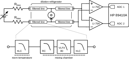
In the main article’s body it has been shown that superconducting-wire SQUIPT magnetometers exhibit very pronounced flux-to-voltage responsivity figures when their current-phase relation transitions from multi-valued to single-valued regime. Here we expand on this application by assessing in detail the magnetometric properties of a complete setup based on this type of device, as illustrated in Figure 1. Notably, the analysis of the cross-correlation between the output signals of two parallel amplification chains connected to the same device allows to distinguish amplifier-limited magnetic flux resolution performance from noise sources intrinsic to the readout scheme.

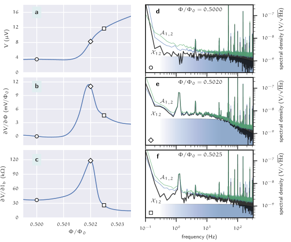
Figure 2 shows a summary of the voltage response of the representative superconducting probe device for $\Phi\approx\Phi_{0}/2$, measured at temperature $T=1\mathrm{K}$ under fixed current $I_{b}=4.35\,\mathrm{nA}$. The noise characteristic of the readout/amplifier system can be assessed by tuning the applied magnetic flux to $\Phi=\Phi_{0}/2$, where the voltage response is null to the first order in $\Phi$. In this configuration (panel d) the power spectral density profiles of the individual preamplifiers (green/blue traces) are only barely higher than their nominal datasheet values, whereas the cross-spectral density (black trace) converges to a profile $\mathcal{X}_{12}(f)$ consistent with the following model (gray shade):

$$\mathcal{X}_{12}(f)=\sqrt{v_{a}^{2}+R_{d}^{2}\,\frac{2eI_{b}}{\left|1+2\pi\mathrm{i}fR_{d}\,\mathcal{C}\right|^{2}}}\quad,$$ (1)

where $v_{a}=0.7\,\mathrm{nV/\sqrt{Hz}}$ is a white noise background, $e$ is the elementary charge, $R_{d}=\partial V/\partial I_{b}$ is the differential resistance and $\mathcal{C}=26\,\mathrm{nF}$ is the effective shunt capacitance consistent with the noise roll-off observed for $f\approx 100\,\mathrm{Hz}$. This simple model, based on the quadrature summation of RC-filtered tunnel shot noise with an amplifier-dependent white noise background is sufficient to describe $\mathcal{X}_{12}$ data recorded for $0.3<f<300\,\mathrm{Hz}$.

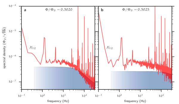
In Figure 2, a comparison between panel b and c shows that the peak in the flux-to-voltage transfer function is associated with a corresponding peak in the differential resistance of the device ($\Phi/\Phi_{0}=0.502$). On the other hand, the latter is suppressed with $\Phi/\Phi_{0}>0.5025$, while the flux-to-voltage transfer function maintains appreciable levels. Panel e shows indeed that at the working point associated with maximal responsivity, the power spectral density of the individual amplifiers is basically indistinguishable from the cross-correlated spectrum, i.e., the $v_{a}$ term is negligible in Equation 1. Here, the high value of $R_{d}$ induces both a reduction in the available bandwidth and an increase of the shot-noise contribution to the observed voltage spectral density. By contrast panel f, corresponding to a working point ($\Phi/\Phi_{0}=0.5025$) characterized by a significantly lower value of $R_{d}$, demonstrates a $\mathcal{X}_{12}(f)$ profile characterized not only by wider available RC bandwith, but also slightly better signal to noise ratio (as suggested by the shape of the $1.3\,\mathrm{Hz}$ signal peak). This difference in performance can be more quantitatively appreciated by renormalizing the spectral density profiles from voltage to magnetic flux units by means of the flux-to-voltage transfer function values. The results are shown in Figure 3. A summary of the performance figures for the different working points is reported in Table I.

$\Phi$ $\partial V/\partial\Phi$ $R_{d}$ noise floor bandwidth
$\Phi_{0}$ mV/$\Phi_{0}$ k$\Omega$ $\mathrm{nV/\sqrt{Hz}}$ $\mathrm{n\Phi_{0}/\sqrt{Hz}}$ $\mathrm{Hz}$
0. 5 0. 0 36. 7 1.5 167
0. 502 11. 3 117. 4.4 390 52
0. 5025 4. 6 26. 2 1.2 260 234
Table 1: Summary of magnetometric figures for the working points in Figure 2.
Refer to caption
Figure 1: Functional schematic of the setup adopted for the characterization of the noise-equivalent flux level of SQUIPT magnetometers. The voltage response of the latter is probed in a 4-wire configuration where the current bias is provided by an adjustable battery-powered voltage source in series with bias resistors $R_{bias}=100\,\mathrm{M}\Omega$. The device is housed in a copper enclosure thermally anchored to the mixing chamber of a helium dilution refrigerator. The latter is equipped with identical electrical DC lines filtered as follows: room-temperature LC($\pi$) lowpass filter (Oxley FLT/P/5000), two-pole RC lowpass (room-temperature values: $R=500\,\Omega$, $C=47\,\mathrm{nF}$) at the mixing chamber followed by high-rejection multistage lowpass (Minicircuits VLFX-80) in series with a LC($\pi$) filter (Oxley SLT/P/5000) at the sample’s enclosure. The magnetic flux $\Phi$ linked to the interferometer loop is applied by a superconducting magnet surrounding the sample stage and powered by a low-noise programmable current source (Keythley model 2600, not shown). The voltage difference across the device is amplified by two separate battery-powered room-temperature differential voltage amplifiers (NF Corporation model LI-75A), whose outputs are digitized independently as the inputs of a vector signal analyzer (HP model 89410A). The latter computes the power spectral density of each input channel as well as the cross-spectral density between them.
Refer to caption
Figure 2: Summary of the magnetoelectric response figure of a typical superconducting-probe device recorded at temperature T=1K and current bias $I_{b}=4.35\,\mathrm{nA}$. The datasets shown here expand on the corresponding data presented in Fig. 4 in the main article’s body. Panels a, b and c show as a function of the applied flux $\Phi$, respectively, the DC voltage, the flux-to-voltage transfer function (obtained by numerical differentiation) and the differential conductance (estimated by finite differences from the voltage traces recorded for $I_{b}=\,4.3,\,4.35,\,4.4\,\mathrm{nA}$). The spectral characteristics of the amplified signal (green/blue traces: individual-channel power spectral density $\mathcal{A}_{1,2}$, black trace: cross-spectral density $\mathcal{X}_{12}$, gray shading: readout noise level estimate) are presented in panels d-f for three illustrative flux working points. Panel d corresponds to zero first-order response ($\Phi/\Phi_{0}=0.5$), while panels e and f are relative to the device being tuned for highest responsivity and best noise-equivalent flux resolution, respectively.
Refer to caption
Figure 3: Cross-spectral density $\mathcal{X}_{12}$ (red trace) and readout noise estimate (gray shading) in magnetic flux units. Panel a and b correspond, respectively, to the device tuned for highest responsivity ($\Phi/\Phi_{0}=0.502$) and for best noise-equivalent flux resolution ($\Phi/\Phi_{0}=0.5025$).